Note: Descriptions are shown in the official language in which they were submitted.
CA 02872020 2014-11-21
SchottAG 20.
November2014
P4146 CA
13SGL0221CAP
DRIVER CIRCUIT WITH A SEMICONDUCTOR LIGHT SOURCE AND METHOD
FOR OPERATING A DRIVER CIRCUIT
SPECIFICATION
Field of the Invention
The invention relates to a driver circuit with a
semiconductor light source, in particular a driver circuit
for a light emitting diode (LED). More particularly, the
invention relates to a driver circuit used for color
controlled LED light sources.
Background of the Invention
Driver circuits for semiconductor light sources, especially
for light emitting diodes, have been known. In particular
color controlled light sources are available. For
controlling the brightness and color of such light sources,
a driver circuit is advantageous which is capable to adjust
the electric power at the light emitting diode over a range
of five orders of magnitude.
Pulse width modulation has been found particularly suitable
for the power control of light emitting diodes, since it
permits to achieve a nearly constant wavelength and an
almost linear behavior in brightness. By contrast, an
adjustment through the current is complex and is moreover
usually quite inaccurate because of the steep diode
characteristic and the non-linear relationship between
current density and brightness.
CA 02872020 2014-11-21
SchottAG 2
20. November2014
P4146 CA
13SGL0221CAP
However, an adjustment through the pulse width is limited.
Very short pulses are difficult to achieve in pulse width
modulation, and moreover they affect EMC behavior.
However, an extension of the pulse intervals is only
possible to a limited extent, since otherwise the distance
between the individual pulses is so long that the human eye
will perceive a flicker. A consequence thereof is that with
a conventional pulse width modulated control the electric
power at the LED can usually only be adjusted over a range
of about three orders of magnitude.
Published patent application WO 2011/114250 Al describes
powering an LED through a power source. When due to dimming
the current falls below a minimum required current value,
the current is kept constant and a pulse width modulated
control is then used. This is associated with an extended
dynamic range which is now only a result of the dynamic
range of the power source and of the pulse width modulated
signal. However, the dynamic range of typical power sources
is limited to 2 to 3 orders of magnitude, since accurate
and at the same time efficient measurement of large and
small currents is only feasible to a limited extent.
Furthermore, it is conceivable to control the LED current
through a step-down converter. Step-down converters are
electrically rather efficient but not designed to provide
very small currents as compared to the maximum current, so
that the dynamic range of a step-down converter is limited
to one to two orders of magnitude.
CA 02872020 2014-11-21
SchottAG 3
20.November2014
P4146 CA
13SGL0221CAP
Moreover, current control relies on a sensing resistor
which, if it is small provides only very small signals at
low currents, or, if it is large leads to severe loss in
efficiency in case of large currents.
A voltage-based adjustment of the power of an LED is
usually not made, due to the steep diode characteristic,
except maybe with very simply designed circuits. In this
case the LED is connected to a relatively large series
resistor, so that the diode characteristic is flattened by
the superimposed characteristic in a manner so that the
current can be adequately controlled through the voltage.
However, such a circuit is inefficient.
Another possibility is to adjust the voltage through
connectable series resistors. However, with the number of
required brightness levels increasing, the number of
required resistors also increases, and moreover the maximum
brightness is quite limited since the behavior of the
current-voltage characteristic is rather inaccurate. In
order to avoid excessive currents which would reduce the
lifetime of the LED, it is therefore necessary to choose a
large series resistor.
Object of the Invention
Therefore, the invention is based on the object to mitigate
the drawbacks of the prior art.
More particularly, an object of the invention is to provide
a driver circuit of a simple configuration, which permits
CA 02872020 2014-11-21
SchottAG 4
20. November2014
P41415CA
13SGL0221CAP
to precisely control the light output of a light emitting
diode over a wide range.
Summary of the Invention
The object of the invention is already achieved by a driver
circuit with a semiconductor light source and by a method
for operating a driver circuit with a semiconductor light
source according to any of the independent claims.
Preferred embodiments and modifications of the invention
are specified by the subject matter of the respective
dependent claims.
The invention relates to a driver circuit with a
semiconductor light source. More particularly, the
invention relates to a driver circuit for light emitting
diodes (LEDs).
Preferably the invention is used for color controlled LEDs.
These especially include so-called RGB LEDs which emit
light in three different colors to be mixed. Such LEDs
permit to efficiently generate light of a desired light
color, in particular white light, for example.
However, a prerequisite for this is a precise control of
the luminous intensities of the individual light colors,
since even small differences in light output will result in
a different color appearance, which is a disadvantage
especially when several of such controlled light sources
are arranged side by side.
CA 02872020 2014-11-21
Schott AG 5
20.November2014
P4146CA
13SG0221CAP
The semiconductor light source is driven through pulse
width modulation. That means, a pulse width modulated
signal is applied to the light source, preferably a square-
wave signal, and the light is adjusted through the duty
cycle, i.e. the ratio of pulse width to pulse interval.
The driver circuit comprises at least one sensor which can
be used to measure the luminous intensity of the light
emitted by the semiconductor light source.
So this sensor measures the brightness of the semiconductor
light source, directly or indirectly.
If a plurality of semiconductor light sources are provided,
it is also possible to measure the brightness of each light
source using a single sensor, by determining the brightness
by means of the sensor during the pulse intervals of the
other semiconductor light sources.
The sensor is connected to a controller. In particular a
microcontroller is used as the controller.
The controller, in turn, controls the luminous intensity of
the semiconductor light source by adjusting the duty cycle
of the pulse width modulation.
It will be understood that the pulse width modulator may be
part of the controller.
According to the invention, the semiconductor light source
is powered by a variable voltage source, and the variable
CA 02872020 2014-11-21
SchottAG 6
20. November2014
P4146CA
13SGL0221CAP
voltage source is controllable by the controller in a
manner so that the voltage applied to the semiconductor
light source is adjustable via the controller when the duty
cycle falls below or exceeds a threshold value.
Here, a variable voltage source does not only refer to a
voltage source for outputting a controlled voltage that is
defined by an input signal.
It may also comprise a fixed voltage source in series with
an adjustable resistor, for example. In such a system the
resistor is selectively varied by an input signal. However,
the effective output voltage depends on the properties of
the downstream circuit. Therefore, a variable voltage
source refers to a circuit unit which supplies a downstream
circuit unit with an effective voltage, wherein the
effective voltage may be increased or decreased in suitable
increments or continuously in response to an input signal
to the voltage source.
According to the invention, therefore, in order to increase
the dynamic range, the voltage is reduced by the controller
when a minimum value of the duty cycle is reached, for
example when the duty cycle falls below 10 %, so that the
pulse widths may be increased in turn.
A determination of the applied voltage or current is not
necessary, since the brightness of the LED will continue to
be accurately controlled by the pulse width modulation.
Preferably, current or voltage control is dispensed with.
So there will be no control loop controlling the current in
CA 02872020 2014-11-21
SchottAG 7
20. November2014
P4146 CA
13SGL0221CAP
a rather complex way or controlling the voltage in a
somewhat less complex, but still complex way. Rather, an
unregulated control element is sufficient, through which
the voltage is varied.
It will be understood that with this unregulated driving of
a control element the voltage source may also be considered
as a current source, since in an electric circuit an
applied voltage is always associated with a current.
The control circuit of the voltage source is therefore
indeterminate. In the context of the invention, the voltage
is furthermore dependent on the operating point of the
electrical components used. The voltage may vary, in
particular due to thermal effects, without this having any
effect on the control according to the invention.
In contrary, the avoidance of a current or voltage control
is rather beneficial for the control according to the
invention, since brightness control is accomplished
indirectly via PWM control which permits to increase or
decrease the voltage when a threshold value is reached
without a need to apply a defined voltage.
In particular no sensing resistor for current control
purposes is required.
However, it may be advantageous if a table of values is
stored in a memory of the controller, which represents the
approximate ratio of applied voltage to brightness.
CA 02872020 2014-11-21
=
Schott AG 8
20. November 2014
P41413CA
13SGL0221CAP
By accessing the table of values, when raising or lowering
the voltage applied to the semiconductor light source the
controller can increase or decrease the duty cycle
accordingly, so that upon switching the brightness remains
essentially the same.
It will be understood that due to the steep diode
characteristic the brightness will usually still change,
however this can be corrected so quickly by the pulse width
modulated control, already at the first pulse or first
several pulses, that an alteration in brightness will not
be visible for the viewer.
In a preferred embodiment of the invention, a variable
resistor is provided for controlling the voltage, which can
be driven by the controller. In particular a digitally
variable resistor is used, which is available as an
integrated circuit and which can be directly controlled by
the digital controller and may optionally be integrated
into the controller, which is provided in form of a
microcontroller.
Furthermore, the variable voltage source may comprise a
transistor, in particular a field effect transistor, more
particularly a MOSFET, which can be driven by the
controller.
In fact a field effect transistor is usually rather
inaccurate, but according to the invention this is
compensated for in a very simple manner by the pulse width
modulation. A significant advantage of a field effect
transistor, besides its availability at a low price, is
CA 02872020 2014-11-21
SchottAG 9
20. November2014
P4146CA
13SGL0221CAP
that it usually has a low resistance. By using a field
effect transistor which changes resistance and hence the
voltage as a function of the voltage applied to the gate,
it is possible to produce such a circuit at low costs and
at the same time to provide for a high efficiency.
The use of a bipolar transistor may also be contemplated,
for example. The latter exhibits higher power loss than a
field effect transistor, and therefore, according to the
invention, it may rather be used to control relatively low
powers.
Furthermore, it is conceivable to use a clocked voltage
converter which is controlled through the clock rate. An
appropriate PWM signal for varying the clock rate may be
supplied from the controller. It will be understood that
this PWM signal does not correspond to the PWM signal for
the LED. A field effect transistor may also be adjusted
incrementally using a digital signal, in particular an
8 bit signal from the controller, specifically 256
resistance values can be set using an 8 bit signal.
Alternatively, a series of resistors may be employed, each
of which may be bypassed independently by a switch and
which add up to a total resistance.
It will be understood that the voltage of the variable
voltage source need not be the only voltage applied to the
semiconductor light source. Rather, it is conceivable to
apply a first voltage to the semiconductor light source,
which is constant and thus defines the minimum voltage. The
CA 02872020 2014-11-21
SchottAG 10
20. November2014
P4146 CA
13SGL0221CAP
voltage controlled through the controller is added and
applied to the semiconductor light source.
The voltage source is preferably adjustable incrementally.
In a preferred embodiment of the invention, the variable
voltage source is adjustable in at least 5, preferably at
least 10, and more preferably at least 100 increments.
To prevent unnecessarily frequent switching between
different voltage ranges, the incremental steps of the
voltage levels and the tolerance ranges of the PWM are
selected such that the expected change in current causes
that the new PWM ratio is again in the center of the
tolerance range.
The voltage change required for this purpose can be seen
from the data sheets of the semiconductor light source, or
can be measured. It will usually not be constant over the
entire range within which the voltage is varied. The
required resistance levels may be calculated from the
required voltage levels for the semiconductor light source
and the base voltage of the voltage source.
For example, if the tolerance range for the PWM duty cycle
is chosen to be from 30 % to 90 %, it follows that a factor
of (90 %/30 %)^-2 - 1.7 causes that when switching the
current level at the threshold, a new operating point is
set at a duty cycle of about 52 %. This duty cycle will
then again be offset from the lower or upper thresholds by
a factor of 1.7. The current increment can be chosen larger
if it is known that continuous brightness ramps are to be
CA 02872020 2014-11-21
SchottAG 11
20. November2014
P4146CA
13SGIA221CAP
driven frequently during operation. In this case, when the
brightness is continuously raised and the maximum duty
cycle it reached, the current will be reduced by a factor
of 2.5, for example, in the above example. This will reduce
the duty cycle to about 35 %, so that when further raising
the brightness the next incremental switching of the level
will be required later than with a factor of 1.7. A similar
consideration applies when decreasing along a brightness
ramp.
If, for example, the voltage is reduced due to a low duty
cycle, then a re-increase in voltage will only be caused
when the associated duty cycle is significantly higher.
The invention further relates to a method for operating a
driver circuit of a semiconductor light source, wherein the
semiconductor light source is driven by pulse width
modulation and the luminous intensity of the light emitted
from the semiconductor light source is sensed by a sensor.
The sensor is connected to a controller which controls the
duty cycle and thus the luminous intensity.
According to the invention, the semiconductor light source
is powered by a variable voltage source which is also
controlled by the controller, and when the duty cycle falls
below or exceeds a duty cycle threshold value, the voltage
applied to the semiconductor light source is increased or
decreased by the controller by driving the variable voltage
source.
CA 02872020 2014-11-21
SchottAG 12
20. November2014
P4146 CA
13SGL0221CAP
Preferably, the voltage applied to the semiconductor light
source is reduced at a duty cycle of less than 30 %,
preferably less than 20 %, in order to be capable to return
to higher duty cycle values.
Furthermore, it is conceivable to increase the voltage at a
duty cycle of more than 70 %, preferably more than 80 %, in
order to be capable to return to lower duty cycle values.
The method may be used to dim a single semiconductor light
source. Preferably, however, the method is used for
controlling the brightness of light emitting devices that
comprise light emitting diodes of different colors.
Description of the Drawings
The subject matter of the invention will now be described
by way of schematically illustrated exemplary embodiments
and with reference to the drawings of Figs. 1 to 4.
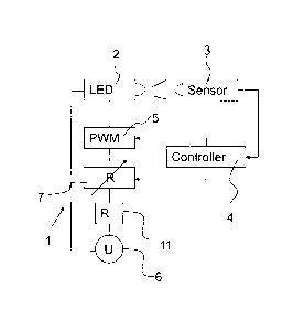
Fig. 1 schematically illustrates a first embodiment of the
invention.
A driver circuit 1 is shown comprising a light emitting
diode 2.
The light emitted by light emitting diode 2 is detected by
a sensor 3, for example a photodiode.
Sensor 3 is connected to a controller 4, which preferably
is configured as a microcontroller.
CA 02872020 2014-11-21
SchottAG 13
20. November2014
P41415CA
13SGL0221CAP
Light emitting diode 2 is driven by pulse width modulation.
For this purpose, a pulse width modulator 5 is provided
which is controlled by controller 4.
It will be understood that the controller 4 may be
connected to external control means (not shown), via which
it receives a signal which represents a desired color of
light (when integrated in a brightness control with a
plurality of differently colored LEDs) and/or a desired
brightness.
Light emitting diode 2 is powered by a voltage source 6. It
will be understood that the voltage source 6 may also
supply a voltage (not shown) for controller 4 or sensor 3.
According to the invention, a variable resistor 7 is
provided, which is also controlled by controller 4. Through
variable resistor 7, the voltage applied at pulse width
modulator 5 can be increased or decreased.
Controller 4 is not connected to a sensing resistor for
sensing the current applied to the LED. Rather, it suffice
to increase or decrease the applied voltage by varying
variable resistor 7. Variable resistor 7 is preferably
provided in form of an integrated circuit and is digitally
controlled.
For example, if the duty cycle is 75 % while sensor 3
signals the controller 4 that the current brightness is
only 0.6 times of the currently desired brightness, the
CA 02872020 2014-11-21
SchottAG 14
20. November2014
P4146 CA
13SGL0221CAP
duty cycle required - in a simplified linear approximation
- would be 75 %/0.6 = 125 %, which is not possible.
The controller now reduces the resistance of resistor 7 by
one increment thereby increasing brightness by 30 %, for
example. Therefore, the duty ratio may also be reduced by
30 %.
This may be accomplished using a table of values which,
however, usually will not lead to the exact desired
brightness but to a substantial approach. Finally, the
brightness will then be adjusted exactly through the pulse
width modulation.
The voltage may preferably controlled incrementally, and in
a preferred embodiment of the invention when changing the
voltage from level to level the brightness changes by less
than a factor of 4, preferably by less than a factor of 2.
The circuit may comprise an invariable series resistor 11
to safely limit the maximum current.
Fig. 2 shows another exemplary embodiment of the invention,
which corresponds to the basic concept of Fig. 1.
Again, a driver circuit 1 is provided, with a light
emitting diode 2 whose luminous intensity is measured by a
sensor 3 and whose light output is controlled by a
controller 4 by driving a pulse width modulator 5.
Again, only a single light emitting diode is shown, whereas
in a preferred embodiment of the invention a plurality of
CA 02872020 2014-11-21
SchottAG 15
20. November2014
P4146 CA
13SGL0221CAP
light emitting diodes are controlled. For this purpose, the
controller 4 would independently control a plurality of
light emitting diodes in different colors.
It is even possible to sense the light from a plurality of
light emitting diodes at the same time using a single
sensor, by having the sensor determining a respective
brightness during the pulse intervals of the other light
emitting diodes. If always at least two light emitting
diodes are turned on, this determination may be made by
addition and subtraction.
Furthermore, it is conceivable to measure the brightness of
different colors of light by differently configured
sensors, for example sensors comprising a color filter.
Controller 4 is connected to the gate of a field effect
transistor 9. In this case the digital signal of controller
4 is converted into an analog voltage signal, by an
internal or external DAC 10. This voltage is used to adjust
the effective resistance of FET 9 between source and drain.
The voltage applied to LED 2 and the current flowing
through LED 2 are a result of the voltage from the voltage
source, the effective resistance of FET 9, and the current-
voltage characteristic of LED 2.
However, measuring or closed loop control of the current or
voltage is not necessary in this case. It must only be
ensured, by a lower limit of the effective resistance, that
the maximum current allowable at the LED 2 is not exceeded.
This may be accomplished by previous calculation
CA 02872020 2014-11-21
= SchottAG
16 20. November2014
P4146 CA
13SGL0221CAP
considering the tolerances of the device, in particular of
the LED, or by calibration.
Furthermore, the circuit may be designed so that the
variable voltage at the gate is superimposed by a base
voltage of a second voltage source 8 which is not
sufficient for through-connecting the FET 9. In this
manner, the entire dynamic range of the DAC 10 may be used
for controlling the resistance.
Moreover, a further ohmic resistor (not shown) may be
connected in series with the FET 9, similar to the
illustration in Fig. 1, which limits the current to the
maximum permissible current through LED 2, even in a fully
through-connected state of FET 9. This increases the safety
of the circuit.
Otherwise, the circuit in which FET 9 supplies a voltage to
the LED via pulse width modulator 5 substantially
corresponds to Fig. 1.
The use of a field effect transistor 9 provides for a
particularly simple digital voltage control.
Referring to Fig. 4, the interaction of the pulse width
modulated control with the voltage control will now be
described.
The voltage should be varied in such a manner that when a
threshold value is reached, the power at the LED is
approximately in a central region of the pulse width
modulation control. If the change in voltage is too large
CA 02872020 2014-11-21
SchottAG 17
20.November2014
P41415CA
13SGL0221CAP
this could cause a switching back and forth between
voltages, and if the change in voltage is too small this
might cause the PWM control to permanently remain near the
thresholds.
Fig. 3 shows the circuit diagram of a further embodiment of
the invention in which a clocked converter 12, in
particular a buck, boost, SEPIC or step-down converter is
used. Converter 12 comprises a field effect transistor
which has a pulse width modulated signal from controller 4
applied to the gate thereof.
This pulse width modulated signal which does not correspond
to the pulse width modulated signal of pulse width
modulator 5 can be used to vary the voltage in the circuit
that includes pulse width modulator 5 and LED 2.
Controller 4 is again connected to sensor 3 and calculates
a first signal for driving the pulse width modulator, and a
second, pulse width modulated signal which is applied to
the gate of the field effect transistor of converter 12.
Fig. 4 shows, on the top, a pulse width modulated signal
which initially has a duty cycle of 100 % which is
associated with a brightness of 100 %.
Further to the right, the duty cycle is reduced to 50 %
corresponding to a brightness of 50 %.
The coordinate system in the middle shows the shortest
switchable pulse at to. It can be seen here, that for the
exemplified light output and the associated duty cycle the
CA 02872020 2014-11-21
SchottAG 18
20. November2014
P41415CA
13SGL0221CAP
pulse interval to the next pulse is very long. This may be
accompanied by a flickering of the light emitting diode.
According to the invention, now, as shown in the coordinate
system on the bottom, the voltage is reduced and hence the
current flowing through the light emitting diode, too. Now,
with the same pulse width a substantially shorter pulse
interval is required in order to obtain the same
brightness.
The invention permits to control LEDs, in particular RGB or
RGBW LEDs, with a higher dynamic range.
CA 02872020 2014-11-21
Schott AG 19
20. November 2014
P4146 CA
13SGL0221CAP
List of Reference Numerals
1 Driver circuit
2 Light emitting diode
3 Sensor
4 Controller
5 Pulse width modulator
6 Voltage source
7 Variable resistor
8 Voltage source
9 Field effect transistor
10 Digital-to-analog converter
11 Resistor
12 Converter