Note: Descriptions are shown in the official language in which they were submitted.
CA 02872076 2014-10-30
1
Luminaire with Leds and Cylindrical Lens
The invention relates to a lamp comprising at least one module having a
plurality of LEDs distrib-
uted over a module surface, whereby multiple LEDs are arranged in a row in a
longitudinal direction
of the module, and whereby multiple of said rows are arranged next to each
other in a transverse
direction of the module that is perpendicular to the longitudinal direction,
and whereby the LED
lamp comprises an optical system for bundling the light emitted by the LEDs.
WO 2012/031703 Al describes a production method for chip-on-board modules, in
which a sub-
strate comprises a plate-shaped carrier having multiple LEDs, whereby a
surface of the substrate is
provided, in an open casting mould, with a cover made up of a layer for
providing an optical system.
The object of the invention is to devise an LED lamp that can be used to
attain homogeneous irra-
diation density in a defined structure.
Said object is met through a lamp comprising
at least one module having a plurality of LEDs distributed over a module
surface,
whereby multiple LEDs are arranged in a row in a longitudinal direction of the
module, and whereby
multiple of said rows are arranged next to each other in a transverse
direction of the module that is
perpendicular to the longitudinal direction,
and whereby the LED lamp comprises an optical system for bundling the light
emitted by the LEDs,
whereby the optical system comprises at least one cylinder lens that extends
in the longitudinal
direction, whereby the light of at least some of the LEDs from a first row of
the rows is bundled into
a line on a target surface by means of the first cylinder lens.
The use of a cylinder lens that extends over at least multiple LEDs allows for
homogeneous bun-
dling of the light of the individual LEDs in an effective manner and with few
components.
In the scope of the invention, a module shall be understood to mean any
spatially-fixed arrange-
ment of a plurality of LEDs. In this context, the module surface shall be
understood to mean a sur-
face connecting all LEDs. In the scope of the invention, the module surface
can just as well corn-
CA 02872076 2014-10-30
2
prise a curvature, for example a barrel-like curvature in the transverse
direction. However, it is pre-
ferred for the module surface to be planar.
The module is generally advantageously, but not necessarily, provided as an
integrated chip-on-
board (COB) module, in which the LEDs and further electronic components, if
applicable, are ar-
ranged on a two-dimensional carrier.
In general, the lamp according to the invention can extend in any way or shape
in particular in the
longitudinal direction. An extension in the transverse direction depends
mainly on the requirements
with respect to the number, power, and intensity of the lines on the target
surface. Regarding the
extension in the longitudinal direction, multiple modules can be arranged one
behind the other de-
pending on the required length, which applies as well analogously to optical
systems that may be
used.
In a generally advantageous refinement of the invention, the optical system
comprises at least a
second cylinder lens that extends in the longitudinal direction, whereby the
light of at least some of
the LEDs from a second row of the rows is bundled into a line on a target
surface by means of the
second cylinder lens. This allows multiple rows of LEDs of the module to be
bundled into lines,
whereby a large opening angle of the lights can be captured and transported in
the transverse di-
rection as well.
In detail, preferably, but not necessarily, the first cylinder lens and the
second cylinder lens bundle
the light into the same line on the target surface. This provides for
particularly intense brightness on
the target surface. The homogeneity of the light intensity along the line can
be further improved
easily in this context, for example through arranging the LEDs of the two rows
at an offset from
each other in the longitudinal direction. Alternatively, or in addition, the
homogeneity can be further
optimised through measures related to the optical system effecting the
bundling.
In a preferred exemplary embodiment of the invention, the optical system
comprises a primary opti-
cal system for bundling the emitted light, whereby the primary optical system
comprises a plurality
of lenses that are arranged right on the LEDs. A primary optical system of
this type can be used to
transport a particularly large spatial angle of the light that is usually
emitted by the LEDs at a large
angle. This can concern, for example, multiple collecting lenses that are each
arranged above an
CA 02872076 2014-10-30
=
3
LED. As a matter of principle, the cylinder lens can also be a component of
the primary optical sys-
tem and can be arranged right above a plurality of LEDs.
Alternatively or in addition to a collecting lens or cylinder lens, the
primary optical system can also
comprise reflectors that are arranged immediately lateral to the LEDs and
further improve a useful
spatial angle range of the transported light. This can concern, for example,
rotationally symmetrical
reflectors that are allocated to individual LEDs.
In a preferred refinement, the primary optical system is provided as a
transparent polymer layer that
is applied to the modules and extends, as one part, over at least multiple
LEDs. A polymer layer of
this type can be provided, for example, according to the optical systems
described in WO
2012/031703 Al. In this context, an LED module is covered with a UV-resistant
silicone in an open
casting mould.
In a preferred refinement of a primary optical system, the lenses that are
arranged above the LEDs
are positioned at a lateral offset in the transverse direction with respect to
a centre of the LEDs.
This enables good bundling of a large opening angle in the transverse
direction when the line of the
target surface is not situated in the geometrical emission direction of the
LEDs of the respective
row. Accordingly, the offset in a preferred refinement can be the larger, the
farther the row of LEDs
is situated from the line in the transverse direction. In particular, a
central row of LEDs may be pre-
sent whose geometrical emission direction intersects with the line, whereby
the lens or lenses of
said row do not comprise an offset.
Advantageously, at least 50% of the light emitted by the LEDs is in a
wavelength range below 470
nm. This allows the lamp to be designed as an UV emitter, at least mainly.
Further combination of
features according to the invention allows the UV emitter to be flexibly
integrated into a technical
device, for example a printing machine.
Alternatively, at least 50% of the light emitted by the LEDs is in a
wavelength range above 780 nm.
This allows the lamp to be designed as an IR emitter, at least mainly. Further
combination of fea-
tures according to the invention allows the IR emitter to be flexibly
integrated into a technical de-
vice, for example a printing machine.
CA 02872076 2014-10-30
4
In a particularly preferred embodiment of the invention, the optical system
comprises a secondary
optical system that is arranged in an optical path of the light while being
spatially separated from
the module. For differentiation from the term of primary optical system, a
secondary optical system
is understood in the present case to generally mean an optical system that is
not positioned right on
the LEDs. Accordingly, embodiments comprising a secondary optical system, but
no primary optical
system, and vice versa are feasible. In a particularly preferred embodiment,
both a primary optical
system and a secondary optical system are arranged in the optical path of the
lamp resulting in a
particularly compact design providing high and homogeneous irradiation
intensity.
According to a preferred design detail, the secondary optical system is
provided as a transparent
polymer layer on a transparent substrate. In this context, the secondary
optical system can be
manufactured like the optical systems described in WO 2012/031703 Al, whereby
a transparent
substrate, for example glass, in place of an LED module, is being covered with
a UV-resistant sili-
cone in an open casting mould.
According to a particularly preferred design detail, the cylinder lens is
provided on the secondary
optical system, which renders the homogeneous bundling of the light emitted by
the LEDs into the
line particularly effective. In this context, it is particularly preferred for
the secondary optical system
to comprise multiple cylinder lenses arranged next to each other in a plane.
Accordingly, each cyl-
inder lens can bundle the light of one of the rows of LEDs or of multiple rows
that are situated next
to each other such that altogether a large number of rows of LEDs can
contribute to the total inten-
sity of the lamp. In particular, the various cylinder lenses can bundle the
light of the LEDs into the
same line.
In a feasible embodiment of the invention, the plane of the cylinder lenses is
inclined with respect to
the module surface and/or target surface. This is a simple way of compensating
an offset between
the line and a position of the module in the transverse direction.
Accordingly, modules can be pro-
vided, for example, in the transverse direction on each side of the line with
each of the modules
being placed in a tilting with respect to a secondary optical system and thus
allowing for particularly
effective bundling into the line. Inclined arrangement of the secondary
optical system or of the
module and the secondary optical system with respect to the target surface is
feasible just as well.
CA 02872076 2014-10-30
A further embodiment of the invention provides a central plane of the row of
LEDs and a central
optical axis, which is situated parallel to the central axis of the row of
LEDs, of a cylinder lens bun-
dling the light of the row to be offset with respect to each other in the
transverse direction. This also
allows simple and effective bundling of a large opening angle into the line to
be attained, in particu-
5 lar when the line is arranged at an offset with respect to the central
plane of the LEDs in the trans-
verse direction. For further optimisation, said offset with respect to an
allocated cylinder lens can
differ for different rows of LEDs depending on the distance of the line from
the row of LEDs in the
transverse direction.
It is generally advantageous for the invention to provide a packing density of
the LEDs in the longi-
tudinal direction to be larger than in the transverse direction. The lower
packing density in the
transverse direction can be balanced through an optimised transport optical
system according to
the invention such that the same intensity on the target surface overall can
be attained with fewer
LEDs. The module can, for example, be a COB module, in which the packing
density is maximal in
the longitudinal direction. This is usually limited by the technical
configuration options of modules of
this type. However, the packing density being maximal in the longitudinal
direction is optimal for the
homogeneity of the intensity distribution over the line. The packing density
in the transverse direc-
tion can, for example, only be 80%, preferably no more than 60%, of a packing
density in the longi-
tudinal direction.
The object of the invention is also met through a device for drying a coating,
comprising a lamp
according to the invention. The lamp according to the invention is
particularly well-suited for this
purpose, since it combines high irradiation intensities and flexible and, in
particular, compact de-
sign.
In a preferred refinement, a two-dimensional substrate bearing the coating to
be dried and the lamp
can be moved towards each other in a conveying direction, whereby the lamp
extends at least
partly over a width of the substrate in a transverse direction and is arranged
at a defined distance
above the substrate. This shall include scanning of the substrate surface in
multiple runs. The sub-
strate can, for example, be printed matter that is coated with lacquer or
another substance being
printed on it in a printing machine.
CA 02872076 2016-05-16
6
The object of the invention is also met through the use of a lamp according to
the invention for dry-
ing a coating, preferably in a printing procedure.
Further advantages and features of the invention are evident from the
exemplary embodiment de-
scribed in the following. In the figures:
Several preferred exemplary embodiments of the invention are described in the
following and illus-
trated in more detail based on the appended drawings. In the figures:
Fig. 1 shows a schematic view through of a first exemplary embodiment of a
lamp according to
the invention.
Fig. 2 shows a schematic arrangement of LEDs of an LED module of the lamp
according to
Fig. 1.
Fig. 3 shows a sectional view in a longitudinal direction of the lamp from
Fig. 1.
Fig. 4 shows a variant of the lamp from Fig. 1.
Fig. 5 shows a view of a second exemplary embodiment of the invention.
Fig. 6 shows a view of a third exemplary embodiment of the invention.
Fig. 7 shows a view of a fourth exemplary embodiment of the invention.
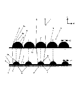
.. A lamp according to the invention according to Fig. 1 comprises an LED
module 1 having multiple
LEDs 3 distributed in an array across a module surface 2 that extends
perpendicular to the plane of
the drawing. The LEDs 3 and further electronic components (not shown) are
attached to a planar
carrier 4, which provides a chip-on-board (COB) module. The module 1 extendls
in a longitudinal
direction L, which extends perpendicular to the plane of the drawing in Fig.
1, and in a transverse
direction W, which extends from top to bottom in the drawing in Fig. 1. A
geometrical main emission
direction H of the LEDs 3 extends perpendicular to the longitudinal direction
L and the transverse
direction W.
The LEDs 3 arranged in the array extend in rows R in the longitudinal
direction, in which they have
a first repeat distance a. In the transverse direction, the rows R are
parallel to each other and have
a repeat distance b. In the present case, approx. ten rows R of LEDs are
arranged next to each
other, not all of which are shown in the drawings.
CA 02872076 2014-10-30
7
The inverse of the repeat distances a, b defines packing densities of the LEDs
in the respective
directions. Presently, the distance a is 2 mm to 5 mm, depending on the
detailed design, whereby
the LEDs have an emitting surface area on the order of approx. 1 mm2. The
distance b typically is
between 5 mm and 10 mm and thus approx. twice the distance a. Accordingly, the
packing density
in the transverse direction W is only half of that in the longitudinal
direction L.
Multiple modules 1 can be arranged one after the other, in particular in the
longitudinal direction,
but also in the transverse direction if needed, depending on the requirements
of the lamp design.
Expediently, the sequential module are appropriately configured with LEDs 3
and/or arranged in
sequence such that the distances of the LEDs are equal and/or such that there
is as little change
as possible in the distribution of the emitted light in the region of the
module limits.
A primary optical system 5 is arranged on the modules 1, which are provided in
the form of a full-
surface coating of the modules 1 in the present case. The primary optical
system 5 comprises
lenses 6, in the form of planar-convex collecting lenses in the present case,
each right on the indi-
vidual LEDs 3, which bundle a large opening angle of the emitted light. This
is associated with pre-
dominant bundling of the beams into a structure in the form of a straight line
on a target surface
(not shown) that extends in the longitudinal direction. The irradiation
intensity on said line afforded
by the lamp clearly exceeds 2 W/cm2.
For purposes of clarification, two extreme-edge optical paths 7 are drawn in
Fig. 1, which converge
and meet further up on the line and/or target surface that is not shown here.
The modules 1 can be arranged on cooling elements (not shown). The cooling
elements preferably
have connectors for inlet and outlet of a liquid coolant that flows through
the cooling elements in
order to dissipate the heat. The coolant can be present in a closed cycle and
release the heat in
another place by means of a heat exchanger. The heat power to be dissipated in
the case of the
present lamp is on the order of significantly more than 1 kW.
In addition to the primary optical system 1, a secondary optical system 8 is
provided upstream of
the modules 1 which further improves the bundling of an exit angle of the LEDs
that is as large as
possible into the structure on the target surface. The secondary optical
system 8 is situated at a
distance upstream of the module 1, but is arranged between the module 1 and
the target surface.
CA 02872076 2016-05-16
=
8
The distance between the secondary optical system 8 and the module surface 2
is significantly
smaller than the distance of the secondary optical system 8 from the target
surface in order to im-
pact the optical path by bundling as early as possible.
The secondary optical system 8 comprises multiple parallel cylinder lenses 9
each that extend in
the longitudinal direction L and are arranged to be parallel to each other in
the transverse direction
W and are arranged in the same plane. Accordingly, at least the light from one
row of LEDs 3 each
is captured through one of the cylinder lenses 9 and bundled into the line
and/or structure of the
target surface 10 (printed matter). Different beams of light of two LEDs are
drawn at different emis-
.. sion angles each in Fig. 1 in exemplary manner and are all bundled into the
same line-shaped
structure on the target surface. In this context, the line has a width Q in
the transverse direction that
is significantly smaller than the distance of the outer rows R of LEDs 3 in
the transverse direction.
In a simplified embodiment of the invention that is not shown here, it is
feasible to forego the sec-
ondary optical system, whereby the cylinder lenses are provided directly in
the primary optical sys-
tem and extend over the individual rows R of LEDs 3.
As is evident from symmetry lines drawn in Fig. 1, there is an is offset V1 in
the transverse direc-
tion in the present case between a centre 3a of the LEDs 3 and a centre 6a of
their lenses 6 of the
.. primary optical system 5.
Moreover, the centres 6a of the lenses 6, just like a central plane and/or
centre 3a of the row of
LEDs 3, have a lateral distance and/or offset V1+V2 in the transverse
direction with respect to a
central optical plane 9a of a cylinder lens 9 bundling the light of said row
R. In this context, V2 is the
offset of the centre 6a of the lenses 6 of the primary optical system with
respect to the central opti-
cal plane 9a of the cylinder lens. Said offset Vi +V2 is the larger, the
farther the respective row R is
offset in the transverse direction with respect to a central plane Z that
coincides with the line of the
target surface. Accordingly, there is no offset for a row R that is arranged
symmetrically on the cen-
tral plane Z (see central row R in Fig. 1).
This is made clear from a comparison of the optical paths of the left outer
row R and the central row
R of LEDs 3 that is arranged in the central plane Z drawn in Fig. 1. The beams
of the peripheral
LEDs must be bundled at an angle to the main emission direction (perpendicular
line onto the mod-
CA 02872076 2014-10-30
=
9
ule surface) in order to hit the line on the target surface. The lateral
offset V1, V2 in each case op-
timises the bundling of an opening angle of the outer LEDs 3, such that it is
as large as possible,
into said optical path.
In the variant shown in Fig. 4, the LEDs 3 and lenses 6, 9 are not situated at
an offset such that the
rows R are bundled into lines on the target surface that are situated next to
each other. Depending
on the sharpness of bundling, said lines may overlap sufficiently such that
overall a relatively broad
line is generated that can be quite homogeneous in the transverse direction as
well.
In the exemplary embodiment of the invention shown in Fig. 5, the secondary
optical system 8 is
provided like in the first exemplary embodiment, whereby all cylinder lenses 9
are situated in a
plane that is parallel to the target surface. Two modules 1 having primary
optical systems 5 are
arranged next to each other upstream of the secondary optical system in the
transverse direction
and are each inclined by the same angle in opposite directions with respect to
the secondary opti-
cal system. Here, a central plane Z extends symmetrically between two cylinder
lenses 9, or, as the
case may be, between one left inner LED 3 of the left module and one right
inner LED 3 of the right
module each. Tilting the modules 1 like in the first example results in
bundling of all rows R of LEDs
into the same line on the target surface.
Unlike the example according to Fig. 5, the example according to Fig. 6
provides a first secondary
optical system 8 to the left of the central plane Z and a second secondary
optical system 8 to the
right of the central plane Z. The secondary optical systems 8 in this case are
arranged to be in-
clined in opposite directions, like the primary optical systems 5, to favour
bundling of the light of the
LED rows R into the same line while keeping the opening angle as large as
possible. In the present
.. case, the primary optical systems 5 and secondary optical systems that are
allocated to each other
each again extend parallel to each other, whereby an inclined arrangement can
be provided just as
well depending on the details of optimisation and the existing requirements.
In the exemplary embodiment according to Fig. 7, unlike the first exemplary
embodiment, additional
reflectors 11 are arranged immediately lateral to the LEDs 3. This guides even
light emitted at very
large angles into the useful optical path. In the present case, the reflectors
11 extend as prismatic
bodies over the longitudinal direction of the module 1, whereby the reflecting
side walls are shaped
to be concave.
CA 02872076 2014-10-30
The primary optical systems in the present case are manufactured according to
a method whose
principles are described in WO 2012/031703 Al through coating the COB modules
with silicone in
an open casting mould. The present secondary optical systems are manufactured
according to an
5 analogous procedure, in which a transparent planar substrate 10, rather
than the COB modules, is
coated with UV-resistant silicone in order to generate the optically active
structures 9 (cylinder
lenses).
A lamp according to the exemplary embodiments described above is used for
purposes of UV dry-
10 ing of lacquer and/or paint in a printing machine, in an offset sheet
printing press in the present
case. An extension of the lamp in the longitudinal direction typically is more
than 1 metre, specifi-
cally 1.6 metres in the present case, which corresponds to the sheet width of
the printed matter. In
order to implement lengths of this order, multiple modules 1 and secondary
optical systems 8 are
typically arranged one after the other in the longitudinal direction.
The lamp components described above are accommodated in a housing (not shown)
that is opti-
mised with respect to the installation space.
An irradiation intensity on the target surface with respect to the
longitudinal direction is approx. 10
Watts per cm in the present case. In this context, most of the light is in a
wavelength range below
470 nm.
In order to manufacture LED lamps with very high optical output power, LEDs of
a size of 0.1-200
mm2, typically 1-2 mm2 are assembled through the chip-on-board procedure
(COB). In this context,
multiple LEDs, typically 4-200 chips, are assembled into a module on a common
substrate having a
surface area on the order of 5 to 50 cm2. The desired lamp length is then
generated by placing
modules configured with LEDs in series.