Note: Descriptions are shown in the official language in which they were submitted.
CA 02872285 2015-03-19
23739-644
1
Circuit board, particularly for a power electronic module, comprising an
electrically-
conductive substrate
Some embodiments of the invention concern a printed circuit board, in
particular for a power electronic module, comprising an electrically
conductive
substrate, wherein the substrate at least partially and preferably completely
comprises aluminum and/or an aluminum alloy. Some embodiments of the invention
further concern a power electronic module including at least one printed
circuit board
and a method of producing a printed circuit board.
The material aluminum is of ever increasing significance in particular in
the field of power electronics. Due to its comparatively low weight and the
low costs
aluminum is frequently used as a cooling body for electronic components (for
example LEDs, IGBTs or MOSFETs) in power electronic modules or directly as
current-carrying conductors, in particular as a current or bus bar. For those
purposes
of use aluminum has a very high level of thermal conductivity and also a very
high
level of electrical conductivity.
In the field of power electronics an insulated metal substrate (referred to
forbrevity as IMS) is frequently used as the substrate, which includes a core
of
aluminum and which is encased by an electrically insulating or dielectric
layer. In that
case the aluminum core is used exclusively for improved heat conduction. The
conductor tracks themselves are arranged on the insulating layer and are not
electrically contacted with the aluminum core.
The object of some embodiments of the invention is to provide a printed
circuit board of the general kind set forth, on which electronic components
can be
arranged to be electrically contactable with a substrate of the printed
circuit board. In
particular some embodiments of the invention seek to provide that an
electronic
component can be soldered to a substrate of a printed circuit board, that
CA 02872285 2015-09-24
23739-644PPH
la
predominantly comprises aluminum and/or aluminum alloy, in order to be able to
. make electrical contacting of the electronic component with the
substrate.
According to one embodiment of the invention, there is provided a
printed circuit board comprising an electrically conductive substrate, wherein
the
electrically conductive substrate at least partially comprises at least one of
aluminum
and an aluminum alloy; wherein arranged on at least one surface of the
electrically
conductive substrate is at least one conductor surface in the form of an
electrically
conductive layer, wherein the conductor surface is directly electrically
contacted with
the electrically conductive substrate; and wherein the electrically conductive
substrate
has a connecting element for connecting the printed circuit board to a direct
current
(DC) voltage source or a three-phase motor.
According to another embodiment of the invention, there is provided a
. power electronic module comprising at least one printed circuit board as
set forth
herein.
According to some embodiments of the invention it is therefore provided
that arranged on at least one surface of the electrically conductive substrate
is at
least one conductor surface in the form of an electrically conductive layer
applied
preferably by a printing process and particularly preferably by a screen
printing
process, wherein the conductor surface is directly electrically contacted with
the
electrically conductive substrate.
CA 02872285 2015-03-19
23739-644
2
An aim of some embodiments of the invention is to achieve direct electrical
contacting of conductor
tracks or conductor surfaces arranged on the substrate with the substrate
itself and to
use the substrate as an electrically conductor. In the case of the proposed
printed .
circuit board an electrically conductive conductor surface which can
substantially
comprise copper and which can be of a thickness of between 25 pm and 125 pm,
preferably between 90 pm and 110 pm, is arranged directly on a surface of the
electrically conductive substrate. It is therefore possible to dispense with
an insulating
layer arranged between the substrate and the conductor surface. That makes it
possible on the one hand to achieve a simplified structure for the printed
circuit board,
whereby a printed circuit board can also be produced at lower cost. On the
other hand
in that way the substrate, in addition to its function as a heat-dissipating
device, can
also be used as the current-carrying part of the printed circuit board. That
is
advantageous in particular in relation to power electronic modules and the
high
electrical currents occurring therein.
According to a particularly preferred embodiment it can be provided that the
at
least one surface of the electrically conductive substrate is substantially
flat. That
makes it possible to substantially simplify the process for producing a
printed circuit
board. Thus for example conventional aluminum plates of a thickness of between
about 1 mm and 3 mm can be easily cut, sawn or stamped out, according to the
respective requirements, without the surfaces of the aluminum plates having to
be
especially treated.
In a preferred embodiment of the invention it can be provided that arranged on
the at least one surface of the electrically conductive substrate is at least
one insulator
surface in the form of a dielectric layer preferably applied by a printing
process and
particularly preferably by a screen printing process. In that respect the at
least one =
insulator surface can at least partially adjoin the at least one conductor
surface, and
can preferably surround the at least one conductor surface.
To prevent flash-over between current- or voltage-carrying parts and a related
short-circuit they must be arranged at a given spacing relative to each other.
For
example the spacing or the air gap between two voltage-carrying parts with a
voltage
= difference of 400 V should be at least 4 mm in accordance with the
Standard DIN EN
60664-1 VDE 0110-1. By virtue of the insulator surface the spacing relative to
other
current-carrying parts, for example other printed circuit boards within a
power electronic
module, with the same dielectric strength, can be reduced, for example to
below 1 mm.
CA 02872285 2014-10-31
3
In that way it is possible to reduce structural sizes of power electronic
modules which
include at least one proposed printed circuit board.
The thickness of the insulator surface can be selected in accordance with the
respective flash-over voltage to be rated. In the case of an average flash-
over voltage
of the dielectric layer of 800 V per 25 pm a thickness of 100 pm for the
insulator
surface is usually sufficient. In general the thickness of the dielectric
layer can be
selected in dependence on the flash-over voltage of an IGBT used and arranged
for
example between two printed circuit boards and for example can be so selected
for
high-voltage applications that a flash-over voltage of between about 600 V and
about
1700 V is achieved.
In general the insulator surface can also serve as a solder covering for the
at
least one conductor surface. Therefore the at least one insulator surface can
be
applied to the substrate in such a pattern so that the at least one conductor
surface or
a plurality of conductor surfaces are surrounded or enclosed by the insulator
surface.
To produce the at least one insulator surface on the substrate it can be
provided that a dielectric layer is applied at least region-wise to the at
least one surface
of the substrate. In that case a dielectric thick-layer paste can be applied
by a printing
process, preferably by a screen printing process. The thick-layer paste can be
dried at
temperatures below about 200 C for about 10 min or sintered directly in a
firing
furnace.
Firing or sintering of the thick-layer paste can be effected in an air
atmosphere
at temperatures of between about 540 C and about 640 C in a firing furnace. It
is also
possible for the thick-layer paste to be fired at temperatures below 540 C but
that can
have a detrimental effect on adhesion of the thick-layer paste to the
substrate. When
the thick-layer paste is fired at over 640 C the substrate can begin to soften
as the
melting point of aluminum is at about 660 C.
To achieve advantageous adhesion of the thick-layer paste to the substrate
glass constituents of the thick-layer paste can include at least one alkali
metal oxide,
for example lithium oxide, sodium oxide or potassium oxide. As a result the
glass
constituents already melt at temperatures below the melting point of aluminum.
In
addition, the coefficient of expansion of the thick-layer paste can be
increased and/or
or adapted to the coefficient of expansion of aluminum, by the presence of
alkali metal
oxides.
A proposed printed circuit board is particularly suitable for being used in
compact power electronic modules, for example in high-current multi-phase
power
CA 02872285 2015-03-19 =
23739-644
4
bridges or inverters. Such power electronic modules frequently employ
electronic
switches or transistors in the form of bipolar transistors with insulated gate
electrodes
(referred as "insulated-gate bipolar transistors" or for brevity IGBT). For
the connection
of such a gate electrode it can be provided that at least one connecting
surface in the
=
form of an electrically conductive layer is disposed on the at least one
insulator surface.
The connecting surface can be subsequently connected to the gate terminal of
an
IGBT, for example by soldering.
A proposed printed circuit board can be part of a power electronic module, for
example of an inverter. Such inverters are used inter alia in hybrid or fully
electric drive
trains in the automobile sector in order to convert the dc voltage of a dc
voltage source
(for example a battery) into a 3-phase ac voltage for a three-phase motor. The
inverter
itself can in that case include six electronic switches (for example IGBTs)
and free-
wheeling diodes corresponding thereto. In that case, by suitable actuation of
the gate
terminals of the IGBTs a dc voltage connected to the inverter, for example in
the range
of between about 300 V and 1200 V, can be converted in known manner into three
phase-displaced ac voltages and fed to a three-phase motor.
According to a particularly preferred embodiment a proposed power electronic
module can include a first printed circuit board, a second printed circuit
board and three
third printed circuit boards.
For the first printed circuit board it can be provided that a plurality of
conductor
surfaces, preferably six conductor surfaces, are arranged on the at least one
surface of =
the electrically conductive substrate, wherein preferably the conductor
surfaces are
surrounded by an insulator surface. For example three IGBTs and three free-
wheeling =
diodes corresponding thereto can be mounted to the conductor surfaces, for
example =
by soldering. The first printed circuit board can be for example in the form
of a
negatively poled current bar of an inverter, that can be connected to the
negative pole
of a dc voltage source.
For the second printed circuit board it can additionally be provided that a
plurality of connecting surfaces, preferably three connecting surfaces, are
arranged on
the insulator surface. In that way, in addition to mounting three IGBTs and
three free- =
wheeling diodes corresponding thereto to the conductor surfaces, the gate
electrodes .
of the IGBTs can also be connected to the connecting surfaces, for example by
soldering, and subsequently actuated. The second printed circuit board can be
for
CA 02872285 2014-10-31
example in the form of a positively poled current bar of an inverter, that can
be
connected to the positive pole of a dc voltage source.
For each of the three third printed circuit boards it can be provided that a
plurality of conductor surfaces, preferably two conductor surfaces, are
arranged on a
5 first surface
of the electrically conductive substrate, and a plurality of conductor
surfaces, preferably two conductor surfaces, and at least one insulator
surface, are
arranged on a second surface of the electrically conductive substrate, wherein
a
connecting surface is arranged on the at least one insulator surface.
Each of the three third printed circuit boards can in that case be in the form
of a
phase connection of an inverter for a three-phase motor. The two conductor
surfaces
of the first surface of a third printed circuit board can in that case be
connected, by
example by soldering, to a respective pair of electronic components ¨
including an
IGBT and a free-wheeling diode corresponding thereto ¨ which can be arranged
on the
second printed circuit board. In that case the two conductor surfaces and the
connecting surface of the second surface of a third printed circuit board can
be
connected, for example by soldering, to a respective pair of electronic
components ¨
including an IGBT and a free-wheeling diode corresponding thereto ¨ which can
be
arranged on the first printed circuit board. The connecting surface can serve
in that
case for respectively connecting the gate electrode of an IGBT.
It has proven to be particularly advantageous if the printed circuit boards
are
arranged substantially stacked, wherein three third printed circuit boards are
arranged,
preferably in mutually juxtaposed relationship, between the first printed
circuit board
and the second printed circuit board. That makes it possible to provide that a
power
electronic module is of a very compact structure.
In a particularly preferred embodiment it can be provided that the power
electronic module is in the form of a high-current multi-phase power bridge,
wherein
three transistors, preferably IGBTs and three free-wheeling diodes are
mounted,
preferably soldered, on the at least one surface of the first printed circuit
board and/or
the second surfaces of the three third printed circuit boards, and wherein
three
transistors, preferably IGBTs and three free-wheeling diodes are mounted,
preferably
soldered, on the at least one surface of the second printed circuit board
and/or the first
surfaces of the three third printed circuit boards.
The operation of soldering electronic components like for example IGBTs and
free-wheeling diodes on a proposed printed circuit board can preferably be
effected by
vapor phase soldering. In that way a unitary temperature gradient can be
achieved in
CA 02872285 2015-03-19
23739-644
6
the solder layers of a power electronic module. In the case of a stacked
inverter a first
solder layer can be arranged between the first printed circuit board and the
three third
printed circuit boards and a second solder layer can be arranged between the
three
third printed circuit boards and the second printed circuit board.
In general a conductor surface can be applied to the surface of a substrate by
various processes like for example by galvanic processes, plasma metal sprays
or by
plating (for example roll plating).
A chemical property of aluminum is a thin oxide layer which is very quickly
formed in the air and which is formed by contact with oxygen in the atmosphere
as a
consequence of an oxidation process at the surface of an aluminum body. That
oxide
layer admittedly affords on the one hand protection from corrosion, but on the
other
hand it causes difficulties in joining aluminum to other materials by
soldering, welding
or other known joining techniques.
For producing a proposed printed circuit board, in particular for producing
the at
least one conductor surface on the substrate, it can therefore be provided
that a
conductor paste is applied at least region-wise to a surface of the substrate,
in a first
firing phase the conductor paste is exposed to a substantially continuously
rising firing
temperature, wherein the firing temperature is increased to a predeterminable
maximum firing temperature of less than about 660 C, in a second firing phase
the
conductor paste is exposed substantially to the predeterminable maximum firing
temperature for a predeterminable period of time, in a cooling phase the
conductor
paste is cooled down and in a post-treatment phase a surface of the conductor
paste is
mechanically post-treated, preferably brushed.
The regions at which the conductor paste is applied and sintered in accordance
with the method steps provide for electrical contacting of the substrate
instead of the
oxidized surface of the substrate, that prevails in that region. That
electrically
conductive layer which is achieved at least region-wise by the application and
sintering
of the conductor paste can be subsequently used for example for soldering an
electronic component or also for soldering a cooling body, wherein the cooling
body =
itself can in turn comprise aluminum.
In that case the substrate can at least partially and preferably completely
comprise an aluminum material with a proportion of aluminum that is as high as
possible. Preferably an aluminum material is used, of the quality EN AW-1050A
or EN
=
CA 02872285 2014-10-31
7
AW-1060A in accordance with European Standard EN 573, containing at least
99.5%
by weight or 99.6% by weight respectively. In spite of somewhat lower liquidus
temperatures and a lower level of thermal conductivity in comparison with the
above-
mentioned substantially pure aluminum materials it is also possible to use
aluminum
alloys, for example aluminum alloys including manganese or magnesium like for
example EN AW-3003 (AlMn1Cu), EN AW-3103 (A1Mn1), EN AW-5005 (A1Mg1) or EN
AW-5754 (AIMg3).
The described production method gives the possible option of selectively
metallizing individual regions of the surface of an aluminum-based substrate,
wherein
the metallized regions are directly connected in the form of sintered
conductor paste to
the substrate in bonded joining of the materials involved and that makes it
possible to
achieve a high level of electrical conductivity and a high level of thermal
conductivity of
conductor paste to substrate and vice-versa. In addition the metallized
regions
represent solderable regions by which the substrate can be connected to
further
components in known fashion. Thus for example individual electronic components
can
be soldered on to the metallized regions using conventional soldering agents
like
eutectic Sn-Pb-, Sn-Ag-Cu- or Sn-Au-solders.
According to a particularly preferred embodiment it can be provided that the
conductor paste is applied to the surface of the substrate by a printing
process,
preferably by a screen printing process.
In that case conventional conductor pastes in the form of thick-layer pastes
or
sinter pastes can be used. Different degrees of heat expansion of conductor
paste and
substrate can be compensated by the porosity of thick-layer pastes, whereby
the
reliability of the connection between the conductor paste and the substrate
can be
increased, in particular in relation to major cyclic thermal stresses as for
example in the
automobile field.
The additive nature of the screen printing procedure with which layers are
built
up on a substrate means it is also possible, for metallizing a substrate
surface, to
dispense with the use of exposure and etching processes, which leads to cost
advantages for the proposed process.
A thick-layer conductor paste usually includes at least a metal powder as an
electrically conductive agent, an inorganic powder (for example glass frits)
as bonding
agent, as well organic binding and dissolving agents. The organic binding and
dissolving agents lead to a paste-like consistency with given rheological
properties,
which however are also influenced by the further constituents of the conductor
paste.
CA 02872285 2014-10-31
8
In regard to the constituent of the electrically conductive metal powder it
can
preferably be provided that a conductor paste including a copper powder is
used. It will
be appreciated however that it is also possible to use a conductor paste
including a
silver and/or gold powder. The use of copper powder is however markedly less
expensive in that respect.
In regard to the constituent of the inorganic powder it can preferably be
provided that a conductor paste including a glass from the Pb0-6203-Si02
system
and/or a glass including Bi203 is used. In that way, during the sintering
procedure in
the proposed method, in spite of the comparatively low firing temperatures
prevailing in
that situation, it is possible to achieve very good adhesion of the conductor
paste to the
substrate.
After a conductor paste is applied by printing, for example by a screen
printing
process known in the state of the art, the conductor paste remains
substantially on the
corresponding regions by virtue of its rheological properties, without flowing
to any
extent worth mentioning. To be able to optimally prepare the conductor paste
applied
to the surface of the substrate for the firing or sintering operation, it can
preferably be
provided that the conductor paste is dried prior to the first firing phase in
a drying phase
at a temperature of between about 80 C and about 200 C, preferably between 100
C
and 150 C, particularly preferably at a maximum of 130 C, preferably for a
period of
between about 5 min and about 20 min. Due to that drying phase the solvents
present
in the conductor paste are substantially completely dissipated. Known drying
methods
like for example infrared or hot air drying are preferred in that case. Due to
the drying
process and the dissipation linked thereto of the solvents in the conductor
paste the
conductor paste experiences a certain volume shrinkage. It is however already
possible to counteract that beforehand by application of the conductor paste
in a
correspondingly thicker layer.
Firing or sintering of the conductor paste in the first and/or second firing
phase
of the proposed method can preferably be effected in a firing furnace, wherein
the firing
temperature prevails in the firing furnace. It will be appreciated that the
drying phase
and/or the cooling phase can also be effected in the firing furnace.
Preferably in that
case a firing furnace having a conveyor device can be used.
In dependence on the material combination used comprising substrate and
conductor paste it is possible to apply a suitable firing profile. A
particular variant
provides that in the first firing phase the firing temperature is increased at
least
temporarily by between about 40 C/min and about 60 C/min. It can further be
provided
CA 02872285 2014-10-31
9
that in the first firing phase the firing temperature is increased to a
maximum firing
temperature of about 580 C, preferably about 565 C, particularly preferably
about
548 C.
Heating the conductor paste to above between about 400 C and 450 C
provides that all organic constituents like for example organic binding agents
are
substantially completely broken up and the inorganic constituents (for example
glass
powder or glass frits) soften. In addition the metal powder sintering process
begins at
those temperatures. The
softened glass constituents of the conductor paste
subsequently lead to good adhesion of the conductor paste on the substrate.
The maximum firing temperature is basically limited by the melting temperature
of aluminum, which is at about 660 C. When using a silver-based conductor
paste the
maximum firing temperature is preferably about 565 C while when using a copper-
based conductor paste the maximum firing temperature is preferably about 548
C.
Those temperatures result from the melting temperatures of possible eutectic
aluminum-copper or aluminum-silver alloys which are involved in that case.
In regard to the respective maximum firing temperature glass constituents
suited to a conductor paste are to be selected, whose corresponding glass
transition
temperature (TG) or melting temperature (Ts) are adapted to that maximum
firing
temperature. The glass transition temperature or melting temperature of the
glass
constituent of the corresponding conductor paste should accordingly be
suitably below
the specified maximum firing temperature to ensure optimum adhesion of the
conductor paste to the substrate. In particular glasses from the Pb0-13203-
Si02 system
or glasses including Bi203 are suitable.
It has proven to be particularly advantageous if firing of the conductor paste
in
the second firing phase is effected for between about 5 min and about 30 min.
It is
possible in that way to achieve optimum adhesion of the conductor paste to the
substrate. Basically, the longer the period of time in the second firing phase
(at
maximum firing temperature), the more densely is the conductor paste sintered
and
thus has better properties for further processing (for example soldering and
welding).
With excessively long periods in the second firing phase however the transit
time in a
typical firing furnace is correspondingly extended in length, which can have
an adverse
effect on the overall through-put.
In a further advantageous embodiment it can be provided that the
predeterminable maximum firing temperature is kept substantially constant in
the
second firing phase.
CA 02872285 2014-10-31
Preferably it can also be provided that the conductor paste is exposed to a
protective gas atmosphere including nitrogen in the first firing phase and/or
the second
firing phase. The use or an inert gas or protective gas means that it is
possible to
reduce or prevent oxidation of a copper contained for example in the conductor
paste.
5 That is advantageous in particular at high temperatures. A protective gas
atmosphere
(for example nitrogen) is advantageous for burning in copper conductor track
pastes to
prevent oxidation of the conductor track material (depending on the firing
phase there
can be a residual oxygen content of some ppm). The organic binders of such a
material or of the conductor paste can be so conceived that they can be
reduced in a
10 nitrogen atmosphere. In turn a conventional air atmosphere can be
advantageous for
silver conductor track pastes because this does not involve any serious
impairment of
the conductor track surface due to oxidation. The organic binders used in that
case
can be oxidized by way of the oxygen in the air.
In a preferred embodiment of the invention it can be provided that in the
cooling
phase the firing temperature is reduced at least temporarily by between about
20 C/min
and about 40 C/min, preferably by about 30 C/min. Preferably in that case
cooling is
effected to ambient temperature. The
slower the cooling operation, the
correspondingly less are the mechanical effects of the join between the
conductor
paste and the substrate by virtue of different coefficients of thermal
expansion of the
materials used.
Due to the typical oxidation of the sintered conductor paste which occurs
during
the firing or sintering process due to the high temperatures prevailing in
that case it is
provided that the surface of the conductor paste is suitably mechanically post-
treated
after the cooling step in order to facilitate further processing, for example
for
subsequent soldering or welding processes.
According to a preferred embodiment it can be provided that the conductor
paste is applied to the surface of the substrate in a thickness of between
about 10 pm
and about 100 pm. It will be appreciated that it is also possible to apply
conductor
pastes to the surface of the substrate in a thickness of less than 10 pm or
conductor
pastes in a thickness of more than 100 pm. It can also be provided that the
proposed
method is applied a plurality of time in succession to increase the overall
resulting
thickness of the conductor paste. Preferably the at least one conductor
surface of the
proposed printed circuit board, that can correspond to the sintered conductor
paste, is
of a thickness of between 25 pm and 125 pm, preferably between 90 pm and 110
pm.
CA 02872285 2015-03-19
23739-644
=
11
Further details and advantages of embodiments of the present invention are
described by
means of the specific description hereinafter. In the drawing:
Figure 1 shows a circuit diagram of a power electronic module in the form of
an
inverter,
Figure 2a shows a perspective view of a proposed printed circuit board,
Figure 2b shows the printed circuit board of Figure 2a with electronic
components arranged thereon,
Figure 3 shows a further proposed printed circuit board with electronic
components arranged thereon,
Figure 4 shows an embodiment of a proposed power electronic module during
assembly,
Figure 5 shows a perspective view of a proposed power electronic module,
Figure 6 shows a side view of a power electronic module as shown in Figure 5,
Figure 7a shows a sectional view along section line I-lin Figure 5,
Figure 7b shows a detail view of Figure 7a,
Figure 8a shows a sectional view along section line 11-11 in Figure 5,
Figure 8b shows a detail view of Figure 8a.
Figure 1 shows a block circuit diagram of a power electronic module 2 in the
form of an inverter. The power electronic module 2 includes six electronic
components =
7 in the form of IGBTs UK, VH, WH, UL, VL, WL and is connected to a dc voltage
source
9, for example a battery. The gate terminals of the three highside transistors
UK, VH,
WH and the three lowside transistors UL, VL, WL are actuated in known manner
by an
electronic actuating means 10 so that the dc voltage of the dc voltage source
9 is
converted by the power electronic module 2 into three phase-displaced ac
voltages and
fed to a three-phase motor 11. Each of the six IGBTs can additionally be
connected to
a corresponding free-wheeling diode. For reasons of clarity of the drawing
however . =
those free-wheeling diodes are not shown in this view.
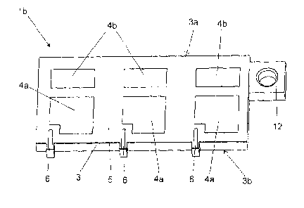
Figure 2a shows a printed circuit board 1b of a power electronic module 2 in
the =
form of an inverter as shown in Figure 1. The printed circuit board lb
includes an
electrically conductive substrate 3 in the form of an aluminum plate, the
surfaces 3a, 3b
of which are substantially flat. The printed circuit board lb can be for
example the
positive current bar of the inverter, that is to be connected to the positive
pole of a dc
voltage source 9 by means of a connecting element 12. The surface 3a of the
printed .
circuit board lb has three conductor surfaces 4a for IGBTs to be arranged
thereon and
three conductor surfaces 4b for free-wheeling diodes to be arranged thereon.
The =
CA 02872285 2014-10-31
12
conductor surfaces 4a, 4b are surrounded or bordered by an insulator surface
5. Both
conductor surfaces 4a, 4b and also insulator surface 5 can be applied to the
surface 3a
of the substrate 3 in the form of suitable thick-layer pastes by means of
screen printing
and can be fired or sintered for example in a firing furnace. To be able to
supply the
gate terminals of the IGBTs with suitable control signals appropriate
connecting
surfaces 6 are additionally arranged on the insulator surface 5.
Figure 2b shows the printed circuit board lb of Figure 2a with IGBTs 7
arranged
on the conductor surfaces 4a and with free-wheeling diodes 8 arranged on the
conductor surfaces 4b. In this case the gate terminals of the IGBTs 7 are
connected to
the connecting surfaces 6.
Figure 3 shows a further printed circuit board la similar to that of Figure 2a
¨
but without gate terminals or connecting surfaces 6 ¨ with IGBTs 7 arranged on
the
conductor surfaces 4a and free-wheeling diodes 8 arranged on the conductor
surfaces
4b. In this case the electronic components 7, 8 are soldered to the
corresponding
conductor surfaces 4a, 4b for example by means of vapor phase soldering.
Figure 4 shows an embodiment of a power electronic module 2 as shown in
Figure 1, wherein the power electronic module 2 includes a first printed
circuit board
la, a second printed circuit board lb and three third printed circuit boards
lc. In this
case the first printed circuit board la corresponds to the printed circuit
board la shown
in Figure 3 and the second printed circuit board lb corresponds to the printed
circuit
board lb shown in Figure 2a. The first printed circuit board la can be
connected for
example to the negative pole of a dc voltage source 9 by means of the
connecting
element 12 of the substrate 3 of the first printed circuit board la, whereby
the substrate
3 of the first printed circuit board la is in the form of a negative current
bar. The
second printed circuit board lb can be connected for example to the positive
pole of a
dc voltage source 9 by means of the connecting element 12 of its substrate 3,
whereby
the substrate 3 of the second printed circuit board lb is in the form of a
positive current
bar.
The three third printed circuit boards lc respectively include an electrically
conductive substrate 3 in the form of an aluminum plate, the surfaces 3a, 3b
of which
are substantially flat. A respective electrically conductive conductor surface
4a for an
IGBT to be connected thereto and an electrically conductive conductor surface
4b for a
free-wheeling diode to be connected thereto are arranged at each first surface
3a of
the substrate 3 of a third printed circuit board lc. Arranged on each of the
second
surfaces 3b of a substrate 3 of a third printed circuit board lc, in addition
to the
CA 02872285 2014-10-31
13
electrically conductive conductor surfaces 4a, 4b, corresponding to the
respective first
surface 3a, is an insulator surface 5, on which an electrically conductive
connecting
surface 6 is arranged for contacting a gate electrode of an IGBT. Each
substrate 3 of
the three third printed circuit boards lc has a connecting element 12, with
which each
of the three third printed circuit boards lc is to be connected to a phase of
a three-
phase motor 11.
As shown in Figure 4, to assemble the power electronic module 2, the printed
circuit boards la, 1 b, lc are stacked vertically one above the other in such
a way that
the three third printed circuit boards lc are arranged in mutually juxtaposed
relationship
between the first printed circuit board la and the second printed circuit
board lb.
Disposed between the first printed circuit board la and the three third
printed circuit
boards 1c are three IGBTs 7 and three free-wheeling diodes 8 which can be
soldered
to the respective conductor surfaces 4a, 4b of the printed circuit boards la,
1c.
Likewise in turn disposed between the three third printed circuit boards 1c
and the
second printed circuit board lb are three IGBTs 7 and three free-wheeling
diodes 8
which can be soldered to the corresponding conductor surfaces 4a, 4b of the
first
surfaces 3a of the third printed circuit boards lc and the first surface 3a of
the second
printed circuit board lb. The gate terminals of the three IGBTs 7 between the
first
printed circuit board la and the three third printed circuit boards lc can be
contacted
by way of the connecting surfaces 6 on the second surfaces 3b of the third
printed
circuit boards lc and the gate terminals of the IGBTs 7 between the three
third printed
circuit boards lc and the second printed circuit board lb can be contacted by
way of
the connecting surfaces 6 of the first surface 3a of the second printed
circuit board lb.
Figure 5 shows a finished assembled power electronic module 2 as shown in
Figure 4 with the difference that an insulator surface 5 in the form of a
dielectric layer
applied by a screen printing process is respectively arranged on both surfaces
3a, 3b
of the three third printed circuit boards lc, wherein the respective insulator
surface 5 of
a surface 3a, 3b surrounds the respective conductor surfaces 4a, 4b. Here in
particular
the vertical stacking of the printed circuit boards la, lb, lc and the compact
structure
of the power electronic module 2 achieved in that way is also apparent.
Figure 6 shows a side view of the power electronic module 2 of Figure 5. The
connecting elements 12 of the substrates 3 of the printed circuit boards la, 1
b, lc form
in this case the connecting points to further components (see Figure 1). In
this
arrangement the connecting element 12 of the first printed circuit board la
can be
connected to the negative pole of the dc voltage source 9 and the connecting
element
CA 02872285 2014-10-31
14
12 of the second printed circuit board lb can be connected to the positive
pole thereof.
The connecting elements 12 of the three third printed circuit boards lc can be
connected to the corresponding phase connections of a three-phase motor 11.
Figure 7a shows a sectional view of the power electronic module 2 of Figure 5
along section line I-I and Figure 7b shows the region B marked with a circle
in Figure
7a on an enlarged scale. The enlarged view in Figure 7b shows an IGBT 7
arranged
between the first printed circuit board la and one of the three third printed
circuit
boards lc of the power electronic module 2. In this case the IGBT 7 is
soldered both
on the conductor surface 4a at the surface 3a of the first printed circuit
board la and
also on the conductor surface 4a at the surface 3b of the third printed
circuit board lc,
for example by means of vapor phase soldering. The solder used in that case is
respectively indicated by reference 13. The conductor surfaces 4a and also the
conductor surfaces 4b (not visible here) on the surface 3a of the first
printed circuit
board la and on the surface 3b of the third printed circuit board lc are
surrounded by a
dielectric insulator surface 5.
Figure 8 shows a sectional view of the power electronic module 2 of Figure 5
along section line II-II and Figure 8b shows the region C marked with a circle
in Figure
8a on an enlarged scale. In comparison with the detail view in Figure 7b it is
possible
to see in the enlarged view of Figure 8b an IGBT 7 arranged between the second
printed circuit board lb and one of the three third printed circuit boards lc
of the power
electronic module 2. The conductor surfaces 4a, 4b on the surface 3a of the
second
printed circuit board lb and on the surface 3a of the third printed circuit
board lc are
surrounded by a dielectric insulator surface 5. The illustrated section along
section line
II-II in Figure 5 is in the region of the gate terminal of the IGBT 7. To be
able to
electrically actuate the gate of the IGBT 7 a connecting surface 6 in the form
of an
electrically conductive layer is arranged on the insulator surface 5 on the
surface 3a of
the second printed circuit board lb. Once again reference 13 denotes the
respective
solder used for soldering the IGBT 7 to the conductor surface 4a of the third
printed
circuit board lc and to the connecting surface 6 of the second printed circuit
board lb.
In the case of a proposed power electronic module 2 with proposed printed
circuit boards la, lb, lc electronic components 7, 8 can be soldered directly
on to the
substrates 3 of the printed circuit boards la, lb, lc by the provision of
solderable
electrically conductive conductor surfaces 4a, 4b. As a result it is possible
to dispense
with other usual connecting procedures like for example wire bonding. By
virtue of the
additional provision of an insulator surface 5 it is possible for the printed
circuit boards
CA 02872285 2014-10-31
la, 1 b, lc to be arranged in a very compact fashion, for example to be
stacked
vertically, without in that respect forfeiting dielectric strength. In the
case of a stacked
structure therefore the spacing between two current- or voltage-carrying
substrates 3 of
printed circuit boards la, lb, lc can be reduced to the thickness of the
electronic
5 components 7, 8 (for example 250 pm of a conventional IGBT 7) and the
thickness of
the conductor surfaces 4a, 4b (for example 100 pm). In the case of a power
electronic
module 2 in the form of an inverter a reduced spacing between the highside
transistors
and the lowside transistors also makes it possible to achieve reduced
inductance of the
power electronic module 2 and thus to increase the efficiency of the power
electronic
10 module 2.
In the production of a power electronic module it can be provided that the
conductor surfaces 4a, 4b and the connecting surface 6 of a printed circuit
board la,
lb, lc are respectively jointly fired or sintered.
In a particularly preferred embodiment it can be provided that the whole,
15 preferably stacked, power electronic module 2 is finished in one working
step insofar as
the components 7, 8 (see Figure 4) arranged between the respective printed
circuit
boards la, lb, lc are soldered in one working step to the respective conductor
surfaces 4a, 4b and connecting surfaces 6 (for example by vapor phase
soldering). It
will be appreciated that it can also be provided that the operation of
assembling the
printed circuit boards la, lb, lc is performed in a plurality of steps. For
example the
electronic components 7, 8 can be respectively soldered to the first printed
circuit board
la and the second printed circuit board lb and in a further step the
electronic
components 7, 8 can be soldered to the corresponding conductor surfaces 4a, 4b
and
connecting surfaces 6 of the third printed circuit boards lc. In that case the
insulator
surfaces 5 of the printed circuit boards la, 1 b, lc can also act as solder
stop masks
which hold the electronic components 7, 8 in the desired positions during a
soldering
operation.
A solder paste to be arranged on the conductor surfaces 4a, 4b can generally
also be used to better orient the substrates 3 of the printed circuit boards
la, 1 b, lc
with each other, insofar as for example layers of differing thickness of
solder pastes are
applied to the conductor surfaces 4a, 4b. In general it is also possible to
use shaped
solder pieces instead of solder paste.
Solders with different melting points can also be used for soldering. Thus for
example an SnAgCu-solder with a liquidus temperature of about 220 C and a high-
lead
solder with a liquidus temperature of about 300 C can be used. As a result for
example
CA 02872285 2014-10-31
16
firstly the electronic components can be soldered with their first sides on
the conductor
surfaces of a substrate with the high-lead solder and fixed there and in a
further step
the electronic components can be soldered with their second sides using the
SnAgCu
solder on the conductor surfaces of a further substrate. Accordingly therefore
the
components can be reliably held in position.
With the proposed printed circuit board it is generally possible to provide a
substrate which in addition to a heat dissipation function also takes over the
function of
an electrical conductor. By applying electrically conductive conductor
surfaces and
dielectric insulator surfaces to the substrate of a proposed printed circuit
board on the
one hand electronic components can be easily soldered to the substrate and
thus
electrically contacted while on the other hand it is possible to achieve
compact
structural configurations for power electronic modules, for example by
vertical stacking.
Spacings of voltage-carrying parts can be reduced and thus the inductance of a
power
electronic module can be reduced by the insulator surfaces. In addition,
direct, double-
sided cooling of a power electronic module can also be achieved by the use of
aluminum as the material for the substrates, and that permits higher current
densities.
By virtue of the provision of solder joins, it is possible to dispense with
other joining
procedures like wire bonding, whereby the reliability of component connections
can be
increased. When using thick-layer procedures for the production of conductor
surfaces
on the substrate of a proposed printed circuit board it is also possible for
the thermal
resistance between an electronic component disposed on the substrate and the
substrate acting as a cooling body to be reduced by the direct assembly of
components
on the substrate, which is made possible in that way. Due to the high porosity
of a
copper conductor paste which is sintered at comparatively low temperatures it
is also
possible to reduce the mechanical stress in a solder layer between a conductor
surface
and an electronic component arranged thereon. That leads in particular to a
higher
temperature cycle resistance and an increased service life.