Note: Descriptions are shown in the official language in which they were submitted.
CA 02872384 2014-10-31
WO 2013/169287 PCT/US2012/061709
PHICH Transmission in Time Division Duplex Systems
BACKGROUND
[0001] As used herein, the term "user equipment" (alternatively "UE") might
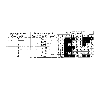
in some
cases refer to mobile devices such as mobile telephones, personal digital
assistants,
handheld or laptop computers, and similar devices that have telecommunications
capabilities. Such a UE might include a device and its associated removable
memory
module, such as but not limited to a Universal Integrated Circuit Card (UICC)
that includes
a Subscriber Identity Module (SIM) application, a Universal Subscriber
Identity Module
(USIM) application, or a Removable User Identity Module (R-UIM) application.
Alternatively, such a UE might include the device itself without such a
module. In other
cases, the term "UE" might refer to devices that have similar capabilities but
that are not
transportable, such as desktop computers, set-top boxes, or network
appliances. The term
"UE" can also refer to any hardware or software component that can terminate a
communication session for a user. Also, the terms "user equipment," "UE,"
"user agent,"
"UA," "user device," and "mobile device" might be used synonymously herein.
[0002] As telecommunications technology has evolved, more advanced network
access
equipment has been introduced that can provide services that were not possible
previously. This network access equipment might include systems and devices
that are
improvements of the equivalent equipment in a traditional wireless
telecommunications
system. Such advanced or next generation equipment may be included in evolving
wireless communications standards, such as long-term evolution (LTE). For
example, an
LTE system might include an Evolved Universal Terrestrial Radio Access Network
(E-
UTRAN) node B (eNB), a wireless access point, or a similar component rather
than a
traditional base station. Any such component will be referred to herein as an
eNB, but it
should be understood that such a component is not necessarily an eNB. Such a
component may also be referred to herein as an access node.
[0003] LTE may be said to correspond to Third Generation Partnership
Project (3GPP)
Release 8 (Re1-8 or R8) and Release 9 (Re1-9 or R9), while LTE Advanced (LTE-
A) may
be said to correspond to Release 10 (Rel-10 or R10) and possibly also to
Release 11 (Rel-
11 or R11) and other releases beyond Release 11. As used herein, the terms
"legacy",
"legacy UE", and the like might refer to signals, UEs, and/or other entities
that comply with
1
CA 02872384 2014-10-31
WO 2013/169287 PCT/US2012/061709
LTE Release 10 and/or earlier releases but do not fully comply with releases
later than
Release 10. The terms "advanced", "advanced UE", and the like might refer to
signals,
UEs, and/or other entities that comply with LTE Release 11 and/or later
releases. While
the discussion herein deals with LTE systems, the concepts are equally
applicable to other
wireless systems as well.
BRIEF DESCRIPTION OF THE DRAWINGS
[0004] For a more complete understanding of this disclosure, reference is
now made to
the following brief description, taken in connection with the accompanying
drawings and
detailed description, wherein like reference numerals represent like parts.
[0005] Figure 1 is a diagram of frequency division duplex and time division
duplex
modes.
[0006] Figure 2 is a table showing LTE time division duplex uplink/downlink
configurations.
[0007] Figure 3 is a diagram of a PHICH modulation process.
[0008] Figure 4 is a diagram of a PCFICH modulation process.
[0009] Figure 5 is a diagram of generation and detection of the PHICH and
the
PCFICH.
[0010] Figure 6 is a diagram of uplink HARQ linkage in inter-band carrier
aggregation
with uplink/downlink configuration 1 on a PCell and configuration 0 on an
SCell.
[0011] Figure 7 is a simplified block diagram of an exemplary network
element
according to one embodiment.
[0012] Figure 8 is a block diagram with an example user equipment capable
of being
used with the systems and methods in the embodiments described herein.
[0013] Figure 9 illustrates a processor and related components suitable for
implementing the several embodiments of the present disclosure.
DETAILED DESCRIPTION
[0014] It should be understood at the outset that although illustrative
implementations of
one or more embodiments of the present disclosure are provided below, the
disclosed
systems and/or methods may be implemented using any number of techniques,
whether
currently known or in existence. The disclosure should in no way be limited to
the
illustrative implementations, drawings, and techniques illustrated below,
including the
exemplary designs and implementations illustrated and described herein, but
may be
2
CA 02872384 2014-10-31
WO 2013/169287 PCT/US2012/061709
modified within the scope of the appended claims along with their full scope
of equivalents.
Embodiments are described herein in the context of an LTE wireless network or
system,
but can be adapted for other wireless networks or systems.
[0015] In an LTE system, downlink and uplink transmissions are organized
into one of
two duplex modes, frequency division duplex (FDD) mode and time division
duplex (TDD)
mode. The FDD mode uses paired spectrum where the frequency domain is used to
separate the uplink (UL) and downlink (DL) transmissions. In TDD systems, on
the other
hand, unpaired spectrum is used where both UL and DL are transmitted over the
same
carrier frequency. The UL and DL are separated in the time domain. Figure 1
illustrates
both duplex modes.
[0016] In a 30PP LTE TDD system, a subframe of a radio frame can be a
downlink, an
uplink or a special subframe. The special subframe comprises downlink and
uplink time
regions separated by a guard period for downlink to uplink switching. 30PP
Technical
Specification (TS) 36.211 defines seven different UL/DL configuration schemes
in LTE
TDD operations. The schemes are listed in Figure 2, where D represents
downlink
subframes, U represents uplink subframes, and S represents a special frame. A
special
frame includes three parts: the downlink pilot time slot (DwPTS), the uplink
pilot time slot
(UpPTS), and the guard period (GP). Downlink transmissions on the Physical
Downlink
Shared Channel (PDSCH) may be made in DL subframes or in the DwPTS portion of
the
special subframe.
[0017] As Figure 2 shows, there are two switching point periodicities
specified in the
LTE standard, 5 milliseconds (ms) and 10 ms. 5 ms switching point periodicity
is
introduced to support the co-existence between LTE and low chip rate UTRA TDD
systems, and 10 ms switching point periodicity is for the coexistence between
LTE and
high chip rate UTRA TDD systems. The supported configurations cover a wide
range of
UL/DL allocations from a DL-heavy 1:9 ratio to a UL-heavy 3:2 ratio. The DL
allocations in
these ratios include both DL subframes and special subframes, which can also
carry
downlink transmissions in the DwPTS. Compared to FDD, TDD systems have more
flexibility in terms of the proportion of resources assignable to uplink and
downlink
communications within a given assignment of spectrum. Specifically, it is
possible to
distribute the radio resources unevenly between the uplink and the downlink.
Such a
distribution may allow the radio resources to be utilized efficiently through
the selection of
3
CA 02872384 2014-10-31
WO 2013/169287 PCT/US2012/061709
an appropriate UL/DL configuration based on the interference situation and
different traffic
characteristics in the DL and the UL.
[0018] The UL and DL transmissions may not be continuous in an LTE TDD
system.
That is, UL or DL transmissions may not occur in every subframe. Therefore,
the data
channel transmissions with their scheduling grant and Hybrid Automatic Repeat
Request
(HARQ) timing relationships are separately defined in the 30PP specifications.
Currently,
the HARQ acknowledgement/negative acknowledgement (ACK/NACK) timing
relationship
for downlink data channel transmission is defined by Table 10.1.3.1-1 in 30PP
TS 36.213.
This timing relationship is shown in Table 1 below. Table 1 associates a UL
ACK/NACK
transmission at sub-frame n, with a DL PDSCH transmission at sub-frames n -
ki, i = 0 to M
-1.
Table 1. Downlink HARQ association set index K. fko,ki,===km_il
UL-DL Subframe n
Configuration
0 1 2 3 4 5 6 7 8 9
0 6 4 - - 6 - 4
1- 7,6 4 - - - 7,6 4 -
2- 8, 7, 4, 6 - -
- 8, 7, 4, 6 -
3- 7, 6, 11 6,5 5,4 -
4 12, 8, 7, 11 6, 5, 4, 7 - - -
-
- - 13,12,9,8,7,5,4,11,6 - - -
6 7 7 5 - - 7 7 -
[0019] The uplink HARQ ACK/NACK timing linkage with the PUSCH transmission
is
listed in Table 8.3-1 of 30PP TS 36.213, which is provided as Table 2 below.
Table 2
indicates that the Physical HARQ Indicator Channel (PHICH) carrying an
ACK/NACK
received in DL sub-frame i is linked with the UL data transmission in UL sub-
frame i - k,
where k is given in Table 2. For UL/DL configuration 0, in sub-frames 0 and 5,
if IPHICH= 1,
then k = 6. Otherwise k = 7. This is because there may be two ACK/NACKs for a
UE
transmitted on the PHICH in subframes 0 and 5.
Table 2. k for Uplink
HARQ ACK/NACK association
TDD UL/DL subframe number i
Configuration 0 1 2 3 4 5 6 7 8 9
0 7 or 6 4 7 or 6 4
1 4 6 4 6
2 6 6
3 6 6 6
4 6 6
5 6
6 6 4 7 4 6
4
CA 02872384 2014-10-31
WO 2013/169287 PCT/US2012/061709
[0020] The relationship of a UL grant and/or an ACK/NACK with a UL
transmission/retransmission is listed in Table 8.2 of 30PP TS 36.213, which is
provided as
Table 3 below. The UE, upon detection of a Physical Downlink Control Channel
(PDCCH)
with Downlink Control Information (DCI) format 0 and/or a PHICH transmission
in sub-
frame n intended for the UE, sends the corresponding PUSCH transmission in sub-
frame n
+ k, where k is given in Table 3.
Table 3. k for Uplink PUSCH grant association
TDD UL/DL subframe number n
Configuration 0 1 2 3 4 5 6 7 8 9
0 4 6 4 6
1 6 4 6 4
2 4 4
3 4 4 4
4 4 4
4
6 7 7 7 7 5
[0021] For TDD UL/DL configuration 0, if the Least Significant Bit (LSB) of
the UL index
in DCI format 0 is set to 1 in sub-frame n or a PHICH is received in sub-frame
n = 0 or 5 in
the resource corresponding to 'PHICH = 1 or a PHICH is received in sub-frame n
= 1 or 6,
the UE sends the corresponding Physical Uplink Shared Channel (PUSCH)
transmission in
sub-frame n + 7 If, for TDD UL/DL configuration 0, both the Most Significant
Bit (MSB)
and the LSB of the UL index in DCI format 0 are set to 1 in sub-frame n, the
UE sends the
corresponding PUSCH transmission in both sub-frames n + k and n + 7, where k
is given in
Table 3.
[0022] It can be seen that both grant and HARQ timing linkage in TDD are
more
complicated than the fixed time linkages used in FDD. Accordingly, TDD usually
requires
more attention in design.
[0023] The PHICH specified in 30PP TS 36.211 is used to transmit a HARQ-
ACK,
which indicates whether the eNB has correctly received UL shared channel (UL-
SCH) data
on the PUSCH. Multiple PHICHs can be transmitted in the same set of resource
elements
as a PHICH group. In the same PHICH group, multiple PHICHs may be multiplexed
with
different complex orthogonal Walsh sequences. In the case of a normal cyclic
prefix, eight
PHICHs can be multiplexed within one PHICH group as the length of the
sequences is four
and the PHICHs are also multiplexed in the complex domain. For an extended
cyclic
5
CA 02872384 2014-10-31
WO 2013/169287 PCT/US2012/061709
prefix, four PHICHs can be multiplexed within a PHICH group with length-2
Walsh
sequences. Figure 3 illustrates the PHICH modulation flow at the eNB.
[0024] For PHICH resource configuration, two parameters are signaled in the
Master
Information Block (MIB): the PHICH duration and the number of PHICH groups.
The
PHICH duration defines the number of Orthogonal Frequency Division
Multiplexing
(OFDM) symbols over which the PHICH is distributed. To avoid a dependency on
the
Physical Control Format Indicator Channel (PCFICH), the PHICH duration is
independently
signaled and can be different from the control region for the PDCCH. The
number of
PHICH groups is used to define the amount of PHICH resources. The
correspondence
between PHICH resources and UL-SCH transmission is implicit. That is, there is
a
predefined representation rule between the PHICH resource index and the PUSCH
Physical Resource Block (PRB) index transmitting the UL-SCH. Because there is
a
PUSCH transmission without a PDCCH in the case of resource non-adaptive
retransmission, a PHICH resource is linked to the actual PUSCH PRB index
instead of the
PDCCH Control Channel Element (CCE) index.
ni3Hr7H
[0025] The PHICH resource is identified by the index pair (nkimi7H,npselcH)
where
is the PHICH group number and npserlicH is the orthogonal sequence index
within the group.
As PHICH resource is implicitly linked to the PUSCH PRB index that is used to
transmit the
corresponding PUSCH, a UE may derive the assigned index pair with the
scheduled
PUSCH PRB index. If a PHICH resource is smaller than the number of PUSCH PRBs
or if
multiple users are scheduled in the same PUSCH PRBs, a collision can happen.
That is,
the same PHICH resource may be assigned to multiple UEs. To avoid a collision,
a
different cyclic shift value that is indicated in the uplink DCI format may be
used to derive
the assigned PHICH resource. The following equations are used to determine the
PHICH
group number and the orthogonal sequence index within the group:
group = (1 lowest index _L
n) group
DMRS oNM + IPHICHNM
=di ploRwBest RAindex 1 Ng3HrolupH] _L
) mod 2N PHICH
PHICH PHICH] DMRS n DMRS , SF
[0026] In the above equations, nDmRs is mapped from the cyclic shift for a
Demodulation
Reference Signal (DMRS) field according to the most recent PDCCH with uplink
DCI
format, as described in 30PP TS 36.212 for the transport block or blocks
associated with
6
CA 02872384 2014-10-31
WO 2013/169287 PCT/US2012/061709
the corresponding PUSCH transmission. DMRS is set to zero if there is no PDCCH
with
uplink DCI format for the same transport block, and if the initial PUSCH for
the same
transport block is semi-persistently scheduled or if the initial PUSCH for the
same transport
block is scheduled by a random access response grant. NalICH is the spreading
factor
size used for PHICH modulation as described in section 6.9.1 of 30PP TS
36.211.
iploRwBesti?Aindex
is the lowest FRB index in the first slot of the corresponding PUSCH
transmission. N '1,111'M is the number of PHICH groups configured by higher
layers as
described in section 6.9 of 30PP TS 36.211.
1 for TDD UL/DL configuration 0 with PUSCH transmission in subfi-amen
=4 or 9
I PHICH =
0 otherwise
=
[0027]
For FDD, the index nZ7H ranges from 0 to NH -1. For TDD, the number of
PHICH groups may vary between downlink subframes and is given by mi = NM where
m, is given by Table 4. The index n1%711 in a downlink subframe with non-zero
PHICH
resources ranges from 0 to mi = NH -1.
Table 4. The factor m, for TDD
Uplink-downlink Subframe number i
configuration 0 1 2 3 4 5 6 7 8 9
0 2 1 - - - 2 1 - - -
1 0 1 - - 1 0 1 - - 1
2 0 0 - 1 0 0 0 - 1 0
3 1 0 - - - 0 0 0 1 1
4 0 0 - - 0 0 0 0 1 1
0 0 - 0 0 0 0 0 1 0
6 1 1 - - - 1 1 - -
1
[0028]
The PCFICH is currently used to indicate the number of OFDM symbols used for
transmission of PDCCHs in each subframe. This number is called the Control
Format
Indicator (CFI). There are three different CFI code words used in the current
version of
LTE and a fourth one is reserved for future use. Each codeword is 32 bits in
length.
Figure 4 illustrates the PCFICH modulation flow at an eNB.
[0029]
In the current LTE specification, the PCFICH and the PHICH use different
resource elements. The PCFICH takes four Resource Element Groups (REGs) and
the
PHICH consumes three REGs. Figure 5 shows the modulation chain at an eNB and
the
demodulation chain at a UE.
7
CA 02872384 2014-10-31
WO 2013/169287 PCT/US2012/061709
[0030] To meet LTE-A requirements, the Rel-10 LTE specification defines
carrier
aggregation (CA) for TDD systems. However, the Rel-10 specification supports
CA only
with the same UL/DL configuration on the aggregated carriers because intra-
band CA is
prioritized, and having different UL/DL configurations is impossible to
support in intra-band
CA, especially when one single RF chain is used.
[0031] To achieve bandwidth flexibility and coexistence with legacy TDD
systems, inter-
band carrier aggregation with different TDD UL/DL configurations on the
carriers from
different bands has been proposed in LTE Rel-11. Many design details, such as
supporting both half duplex and full duplex modes, supporting both separate
scheduling (s-
scheduling) and cross-carrier scheduling (c-scheduling), transmitting the
PHICH on the cell
carrying the UL grant, and transmitting the PUCCH only on the primary cell,
have been
agreed upon. Some agreements have also been reached on HARQ timing linkage.
[0032] It should be noted that a component carrier (CC) is also known as a
serving cell
or a cell. Furthermore, when multiple CCs are scheduled, for each UE, one of
the CCs is
designated as the primary carrier which is used for PUCCH transmission, semi-
persistent
scheduling, etc., while the remaining CCs are configured as secondary CCs.
This primary
carrier is also known as a PCell (Primary cell), while the secondary CC is
known as an
SCell (Secondary cell).
[0033] As discussed above, the timing linkage in TDD systems is not as
simple as in
FDD systems. The degree of complexity increases when CA with different TDD
configurations is considered. This is because, with different TDD
configurations, there are
some time instances with conflicting subframes among aggregated CCs. For
example, a
UL subframe on CC1 may occur at the same time that CC2 has a DL subframe.
Also, the
timing linkage may be different for each different TDD configuration and,
furthermore,
certain control signals may have to be on a specific carrier. For example, the
PHICH may
have to be transmitted on the cell carrying the UL grant. These conditions may
lead to a
need to transmit a PUSCH ACK/NACK at a DL subframe that does not have a PHICH
resource configured according to Table 4 above.
[0034] One of the 30PP design agreements indicates that the PHICH can be
transmitted only on the cell carrying the UL grant in the case of inter-band
CA with different
UL/DL configurations. Therefore, a PUSCH ACK/NACK may need to be transmitted
at a
DL subframe that does not have a PHICH resource configured.
8
CA 02872384 2014-10-31
WO 2013/169287 PCT/US2012/061709
[0035] In an example case, two TDD carriers may be aggregated, the PCell
may be set
as UL/DL configuration 1, and the SCell may have UL/DL configuration 0, in
full duplex
mode. Based on the 30PP design principles, the PCell follows its own UL HARQ
timing
relationship, which is configuration 1, and the SCell UL HARQ follows the
timing of
configuration 0. In this case, the PCell with UL/DL configuration 1 is the
scheduling cell
and carries the UL grant for the SCell, so the PUSCH ACK/NACK should be on the
PCell
as well. Figure 6 illustrates the UL HARQ timing of the above scenario. The
solid arrows
represent the SCell UL grant for transmission/retransmission, and the dashed
arrows
represent the UL HARQ-ACK timing of the SCell.
[0036] It can be seen that the ACK/NACK for PUSCH transmission at subframe
#3 or
#4 of the SCell should be at subframe #0 of the PCell. However, with UL/DL
configuration
1, referring to Table 4 above, there is no PHICH resource provisioned in the
control region
of PCell subframe #0. The same issue occurs for the PUSCH transmission at
subframes
#8 and #9 of the SCell. Additionally, there is no PHICH resource provisioned
at subframe
#5 of the PCell.
[0037] Embodiments of the present disclosure can resolve these PHICH
resource
issues by multiplexing the PHICH onto PCFICH resource elements. The extra
PHICH
resources created by multiplexing the PHICH for the carrier aggregation UEs
onto the
PCFICH provide the capability to convey up to six ACK/NACKs using PCFICH
resource
elements. These extra PHICH resources are recognized only by CA UEs, that is,
UEs
capable of operating under a carrier aggregation scenario. Legacy UEs can
still use the
same resources defined in Rel 8/9/10. Therefore, these embodiments are fully
backward
compatible.
[0038] In some cases, these embodiments may be used in conjunction with an
adaptive
retransmission procedure. In these cases, retransmission is directly triggered
by a UL
grant if there is a need for PUSCH retransmission. In this way, there is no
need for an
ACK/NACK transmission if there is no PHICH resource provisioned in some DL
subframes.
9
CA 02872384 2014-10-31
WO 2013/169287 PCT/US2012/061709
[0039] In PCFICH generation, the scrambled bits are given by:
g (CFI) () (b
b(CFI =
) (I) C(0)M0d2 (1)
where b(cm(i)E {OM denotes the i-th bit in a CFI sequence for a given CFI
value; WO}
denotes the scrambling sequence initialized with cilia = Qns/2] + 1) =
(2NieDell +4 29 NiDeen
at the start of each subframe; and g(cH)(0 is the i-th scrambled bit.
[0040] Quadrature phase shift keying (QPSK) modulation is used to generate
a block of
16 complex-valued symbols {d(k), k = 0, 1, ...,15}.
Table 5. QPSK modulation mapping
I
00 1/5 1/5
01 1/5 -1/5
-1/5 1/5
11 -115 -1/5
[0041] It can be shown that the modulated PCFICH symbols can be written
into the
following form:
1
d(PCFICH) (k) = ¨21 = b(c") (2k)) = (1 ¨ 2 = c(2k)) +
1 k=0,1,2,...,15
(2)
j (1¨ 2 b(c") (2k +1)) =
(1 ¨ 2 = c(2k +1))
CA 02872384 2014-10-31
WO 2013/169287 PCT/US2012/061709
[0042] A PCFICH detection in general is a reversed operation of the PCFICH
generation to find the one with the maximum energy of the following possible
RxCFI
correlations:
- 2
(RxCFI) =
LRe{x(PcFicro(k)} = (1¨ 2 = b(RxcH) (2k)) = (1¨ 2 = c (2k)) +
_k=0
-2
15 (3)
Lim{ x(PCFICH) (k)1 = (1 ¨ 2 = b(RxCH) (2k + 1)) = (1 ¨ 2 = c(2k + 1)) ,
_ k=0
RxCFI = 0,1,2
where x(PCFICH )(k) denotes the received signal at PCFICH RE k. It may be
noted that
x(PCFICH ) (k) = d (PCFICH )
(k) in an ideal channel (no noise, no fading, and no phase rotation).
Also, it is possible to add the real and imaginary parts and then take the
square instead of
taking the squares separately and then summing.
[0043] The detected CFI is given by:
g max ( y (RxCH) )
CFI detected = ar (4)
RxCHE{ 0,1,2}
[0044] For the PHICH, the channel coding will generate a total of 12 coded
bits with
three repeated sections, each section having a length of four. Each PHICH
ACK/NACK bit
will be repeated 12 times and then be binary phase shift keying (BPSK)
modulated,
scrambled, and cover-coded with the PHICH orthogonal sequence. For a given
PHICH
sequence, the resulting symbols are given by:
d(PHICH) (k) = (1 j) w(seqldx) (1-2. b(HI ,se gay) (0) = (1 ¨ 2. c(k)) ,
112
(5)
k=0,1,2,...,11 (normal CP)
k=0,1,2,...,5 (extended CP)
(seqldx)
where Wk is the k-th element in the three-times-repeated orthogonal
sequence with
sequence index seqldx; b(HI 'segicix) (k) is a HI bit (for ACK/NACK)
associated with
sequence index seqldx; and c(k) is a cell-specific scrambling sequence that is
the same
as that used for PCFICH generation.
[0045] The three-times-repeated orthogonal sequence is formed by repeating
the
complex orthogonal Walsh sequence [w(0) === w(vancll -1)] three times and
concatenating
the sequences together. The complex orthogonal Walsh sequence is given by
Table 6
11
CA 02872384 2014-10-31
WO 2013/169287 PCT/US2012/061709
below, where the sequence index seqldx = ripsexclicH corresponds to the PHICH
number
within the PHICH group.
Table 6. Orthogonal sequences [w(o) = = = w(NallCH ¨1)] for PHICH.
Sequence index Orthogonal sequence
seq Normal cyclic prefix Extended cyclic prefix
nPHICH N PHICH ancx = 4
NSF = 2
0 [+1 +1 +1 +11 [+1 +I]
1 [+ -1 +1 -1] ki -1]
2 [+1 +1 ¨1 -1] [ti +11
3 ]+1 -1 -1 +11 [
4 [+1 +1 +1 +11
5 [+1 ¨j +1 ¨11
6 [+1 +1 ¨j ¨11
7 [+1 ¨j ¨j +11
[0046]
The transmitted PHICH symbols are a summation of PHICH symbols for multiple
PHICH sequences in one PHICH group.
[0047]
PHICH detection involves extracting the transmitted PHICH information from the
received channel-equalized symbols. Given a set of received symbols {x(k)},
the decision
variable for PHICH sequence RxSeqIdx can be written in the following form:
y(Rxsegich) = Re {(1 +pH (W k(se" )H (1-2. c(k)) x(k)} ,
(6)
k=0,1,2,...,11 (normal CP)
k=0,1,2,...,5 (extended CP)
where the superscript H denotes a matrix Hermitian operation, which is equal
to a
conjugate transpose.
[0048]
By comparing PCFICH generation Equation (2) and PHICH generation Equation
(5), a sequence of PHICH symbols orthogonal to the sequence of PCFICH symbols
in
Equation (2) can be formulated by removing the BPSK modulation factor of (1+j)
from
Equation (5), replacing (1- 2. c(k)) by (1-2. b(CFI) (2k))= (1-2. c (2k)) for
real-valued
(seqldx)
Wk
, replacing (1-2. c(k)) by (1¨ 2 = b(cm (2k +1)) = (1¨ 2 = c(2k +1)) for
imaginary-valued
12
CA 02872384 2014-10-31
WO 2013/169287 PCT/US2012/061709
(seqldx)
Wk and extending the length of PHICH spreading to 16 by repeating the HARQ
,
indicator and Walsh sequence four times instead of three times.
[0049] The resulting PHICH symbols are given by:
i is real
d(pracH ) ( = I/ 2
(7)
' 1 nl w Isegrax) 0 ¨2. b(HI ,seqIdx) (0) . 0 _ 2 b
. (CH ) (2k)) .
¨2. b(1 H , seqIdx ) (0) . (1_ 2 . b(cR)(2k _F:.2
1/2 (1 ._c2(2. k), c:
ifw'Iseg')
0
2k +1)), otherwise
[0050] If Equation (7) is compared with Equation (2), it can be seen that
Equation (7)
can be viewed as a generalized extension of the real or imaginary part of
Equation (2) with
an additional layer of covering code Wk(seqldx) 0 _ 2 . b(HI,seqldx) (k)) \ .
On the other hand,
'seqmx)
Wk
.seq
Equation (2) is a special case of Equation (7) when b ldv)
(k) = 0 and
[1,1,1,1...] combined with the case when b(Hi'segicix)(k) = 0 and iv k(seqldv)
. [i,j,i,j...1. If an
orthogonal Walsh sequence from Table 6, except sequence number 0 [1,1,1,1] and
sequence number 4 [j,j,j,j] for normal CF or sequence number 0 [1,1] and
sequence
number 2 [j,j] for extended CP, is used in Equation (7), and if the CFI
hypothesis is correct,
the sequence of PHICH symbols defined in Equation (7) is orthogonal to the
sequence of
PCFICH symbols defined in Equation (2).
[0051] As a result, the PHICH symbols defined in Equation (7) can be
transmitted on
top of PCFICH symbols defined in Equation (2) such that the PHICH and the
PCFICH
share the same set of resource elements. This may be useful in subframes where
there is
no provisioned resource for the PHICH.
[0052] Since the newly added PHICH symbols are differentiated by the Walsh
code and
orthogonal to the PCFICH symbols, this solution is backward compatible. Legacy
UEs are
still able to decode the PCFICH. According to CFI detection with Equations (3)
and (4) and
the orthogonality of the Walsh code, if the CFI hypothesis is correct, the
overlay PHICH
transmission does not affect PCFICH correlation in additive white Gaussian
noise (AWGN)
or when the frequency selectivity of the channel is not as severe. However,
this overlay
PHICH transmission may or may not increase the correlation value of the CFI
detection
using Equations (3) and (4), when the CFI hypothesis is not correct. This may
slightly
decrease the CFI detection performance. As the orthogonality of the Walsh code
defined
13
CA 02872384 2014-10-31
WO 2013/169287 PCT/US2012/061709
in Table 6 needs to be maintained just in one REG, and the four resource
elements (REs)
of one REG are closely located, it is expected that, in frequency selective
fading channel
cases, this solution will have only a limited performance degradation compared
to the flat
channel case. This performance degradation can be overcome by slightly
increasing the
transmit power on the PCFICH transmission.
[0053] CA UEs could make use of the extra power corresponding to the PHICH
transmission to improve their PCFICH detection.
[0054] After the PCFICH is correctly detected, the PHICH can be detected,
similarly to
Equation (6), by the following equation:
Re{ I (w' )H (1 ¨ 2 = b(cH)(2k)) = (1-2. c(2k)) x(k)}, if wi(csegli') is real
(Rxseqldx) = k
Y,
Re{ I (w' )H (1 ¨ 2 = b(cH)(2k +1))= (1-2. c(2k +1)) x(k)}, otherwise
k
[0055] In above equation, (1¨ 2 = b(cm (2k))= (1¨ 2 =
c(2k)) or
(1¨ 2 = b(cm (2k +1)) = (1¨ 2. c(2k +1)) can be treated as new scrambling
sequences for the
overlay PHICH transmission.
[0056] To achieve orthogonality between the overlaying PHICH transmission
and the
PCFICH transmission, it can be seen that the number of sequences available to
carry
PHICH bits is reduced to six from eight. This solution enables an eNB to
multiplex six
PUSCH HARQ indicators onto a PCFICH channel without using any extra resource
elements. The peak to average power ratio (PAPR) in this combined PCFICH and
PHICH
is no worse than in the existing PHICH.
[0057] In an embodiment, since there is only one PHICH group in this case
and only six
PHICHs available, the mapping between the PUSCH and these new PHICHs may be
given by:
nseq = (powest Index + n ) mod N
PHICH PRB RA DMRS
where N is 6 for a normal cyclic prefix and 2 for an extended cyclic prefix.
The other
variables use the same notation as above.
14
CA 02872384 2014-10-31
WO 2013/169287
PCT/US2012/061709
[0058] The sequence index seqldx = n Ps el-cllICH corresponding to the
PHICH number is
given by Table 7.
Table 7.
Proposed orthogonal sequence to PHICH sequence index mapping.
Sequence index Orthogonal sequence
seq Normal cyclic prefix Extended cyclic prefix
nPHICH PHICH A T PHICH = 2
0 [+i ¨1 +1 ¨1] k 1 ¨1]
1 kl +1 ¨1 ¨1] [ j -ji
2 [-F1 ¨1 ¨1 +11
3 [-Hi -j +j -11 -
4 [-Hi +j -j -11 -
5 [-Hi -j -j +11 -
[0059] Alternatively, explicit signaling can be used to define the mapping
between the
PUSCH and these new PHICH bits.
[0060] In an embodiment, if there are more than six PHICH bits, the first
six bits can
use the approach described above and the rest can rely on an adaptive
retransmission
procedure. The adaptive retransmission procedure uses a UL grant to instruct
UEs
regarding PUSCH retransmission. ACK/NACK information can be implicitly
conveyed in
this procedure, so there is no need for ACK/NACK transmission in DL subframes.
Legacy
UEs will not be impacted, since this procedure is UE-specific. Moreover,
legacy UEs could
also use this scheme if needed.
[0061] In an embodiment, the UL grant uses DCI format 0 transmitted in the
PDCCH
and contains a New Data Indicator (NDI). Whenever a new packet transmission
begins,
the one-bit NDI is toggled. For indication of retransmission, the one-bit NDI
is kept at the
same value as in the previous DCI 0 grant for the same HARQ process. The UE
receives
the UL grant and compares the NDI with the previously received grant's NDI. If
the NDIs
are the same, the UE knows that the UL grant is for the retransmission of the
UL-SCH data
on the previous PUSCH.
[0062] With adaptive retransmission, the retransmission Physical Resource
Block
(PRB) can be different from the initial PUSCH PRB. This provides an
opportunity to
choose more desirable radio resources based on the current radio channel
conditions and
may lead to better performance. However, since the UL grant is UE-specific, it
may
become costly, in terms of PDCCH resources, if there are a significant number
of
CA 02872384 2014-10-31
WO 2013/169287 PCT/US2012/061709
retransmissions relying on this scheme. Operators could apply a policy to
restrict the
feature to important users with high quality of service requirements.
[0063]
The above may be implemented by a network element. A simplified network
element is shown with regard to Figure 7. In Figure 7, network element 3110
includes a
processor 3120 and a communications subsystem 3130, where the processor 3120
and
communications subsystem 3130 cooperate to perform the methods described
above.
[0064]
Further, the above may be implemented by a UE. An example of a UE is
described below with regard to Figure 8. UE 3200 may comprise a two-way
wireless
communication device having voice and data communication capabilities. In some
embodiments, voice communication capabilities are optional. The UE 3200
generally has
the capability to communicate with other computer systems on the Internet.
Depending on
the exact functionality provided, the UE 3200 may be referred to as a data
messaging
device, a two-way pager, a wireless e-mail device, a cellular telephone with
data
messaging capabilities, a wireless Internet appliance, a wireless device, a
smart phone, a
mobile device, or a data communication device, as examples.
[0065]
Where the UE 3200 is enabled for two-way communication, it may incorporate a
communication subsystem 3211, including a receiver 3212 and a transmitter
3214, as well
as associated components such as one or more antenna elements 3216 and 3218,
local
oscillators (L0s) 3213, and a processing module such as a digital signal
processor (DSP)
3220. The particular design of the communication subsystem 3211 may be
dependent
upon the communication network in which the UE 3200 is intended to operate.
[0066]
Network access requirements may also vary depending upon the type of
network 3219. In some networks, network access is associated with a subscriber
or user
of the UE 3200. The UE 3200 may require a removable user identity module
(RUIM) or a
subscriber identity module (SIM) card in order to operate on a network. The
SIM/RUIM
interface 3244 is typically similar to a card slot into which a SIM/RUIM card
may be
inserted. The SIM/RUIM card may have memory and may hold many key
configurations
3251 and other information 3253, such as identification and subscriber-related
information.
[0067]
When required network registration or activation procedures have been
completed, the UE 3200 may send and receive communication signals over the
network
3219.
As illustrated, the network 3219 may consist of multiple base stations
communicating with the UE 3200.
16
CA 02872384 2014-10-31
WO 2013/169287 PCT/US2012/061709
[0068]
Signals received by antenna 3216 through communication network 3219 are
input to receiver 3212, which may perform such common receiver functions as
signal
amplification, frequency down conversion, filtering, channel selection, and
the like. Analog
to digital (AID) conversion of a received signal allows more complex
communication
functions, such as demodulation and decoding to be performed in the DSP 3220.
In a
similar manner, signals to be transmitted are processed, including modulation
and
encoding for example, by DSP 3220 and are input to transmitter 3214 for
digital to analog
(D/A) conversion, frequency up conversion, filtering, amplification, and
transmission over
the communication network 3219 via antenna 3218. DSP 3220 not only processes
communication signals but also provides for receiver and transmitter control.
For example,
the gains applied to communication signals in receiver 3212 and transmitter
3214 may be
adaptively controlled through automatic gain control algorithms implemented in
DSP 3220.
[0069]
The UE 3200 generally includes a processor 3238 which controls the overall
operation of the device.
Communication functions, including data and voice
communications, are performed through communication subsystem 3211. Processor
3238
also interacts with further device subsystems such as the display 3222, flash
memory
3224, random access memory (RAM) 3226, auxiliary input/output (I/0) subsystems
3228,
serial port 3230, one or more keyboards or keypads 3232, speaker 3234,
microphone
3236, other communication subsystem 3240 such as a short-range communications
subsystem, and any other device subsystems generally designated as 3242.
Serial port
3230 may include a USB port or other port currently known or developed in the
future.
[0070]
Some of the illustrated subsystems perform communication-related functions,
whereas other subsystems may provide "resident" or on-device functions.
Notably, some
subsystems, such as keyboard 3232 and display 3222, for example, may be used
for both
communication-related functions, such as entering a text message for
transmission over a
communication network, and device-resident functions, such as a calculator or
task list.
[0071]
Operating system software used by the processor 3238 may be stored in a
persistent store such as flash memory 3224, which may instead be a read-only
memory
(ROM) or similar storage element (not shown). The operating system, specific
device
applications, or parts thereof, may be temporarily loaded into a volatile
memory such as
RAM 3226. Received communication signals may also be stored in RAM 3226.
17
CA 02872384 2014-10-31
WO 2013/169287 PCT/US2012/061709
[0072]
As shown, flash memory 3224 may be segregated into different areas for both
computer programs 3258 and program data storage 3250, 3252, 3254 and 3256.
These
different storage types indicate that each program may allocate a portion of
flash memory
3224 for their own data storage requirements. Processor 3238, in addition to
its operating
system functions, may enable execution of software applications on the UE
3200. A
predetermined set of applications that control basic operations, including at
least data and
voice communication applications for example, may typically be installed on
the UE 3200
during manufacturing. Other applications may be installed subsequently or
dynamically.
[0073]
Applications and software may be stored on any computer-readable storage
medium. The computer-readable storage medium may be tangible or in a
transitory/non-
transitory medium such as optical (e.g., CD, DVD, etc.), magnetic (e.g.,
tape), or other
memory currently known or developed in the future.
[0074]
One software application may be a personal information manager (PIM)
application having the ability to organize and manage data items relating to
the user of the
UE 3200 such as, but not limited to, e-mail, calendar events, voice mails,
appointments,
and task items. One or more memory stores may be available on the UE 3200 to
facilitate
storage of PIM data items. Such a PIM application may have the ability to send
and
receive data items via the wireless network 3219. Further applications may
also be loaded
onto the UE 3200 through the network 3219, an auxiliary I/O subsystem 3228,
serial port
3230, short-range communications subsystem 3240, or any other suitable
subsystem
3242, and installed by a user in the RAM 3226 or a non-volatile store (not
shown) for
execution by the processor 3238. Such flexibility in application installation
may increase
the functionality of the UE 3200 and may provide enhanced on-device functions,
communication-related functions, or both.
For example, secure communication
applications may enable electronic commerce functions and other such financial
transactions to be performed using the UE 3200.
[0075]
In a data communication mode, a received signal such as a text message or
web page download may be processed by the communication subsystem 3211 and
input
to the processor 3238, which may further process the received signal for
output to the
display 3222, or alternatively to an auxiliary I/O device 3228.
[0076]
A user of the UE 3200 may also compose data items, such as email messages
for example, using the keyboard 3232, which may be a complete alphanumeric
keyboard
18
CA 02872384 2014-10-31
WO 2013/169287 PCT/US2012/061709
or telephone-type keypad, among others, in conjunction with the display 3222
and possibly
an auxiliary I/O device 3228. Such composed items may then be transmitted over
a
communication network through the communication subsystem 3211.
[0077] For voice communications, overall operation of the UE 3200 is
similar, except
that received signals may typically be output to a speaker 3234 and signals
for
transmission may be generated by a microphone 3236. Alternative voice or audio
I/O
subsystems, such as a voice message recording subsystem, may also be
implemented on
the UE 3200. Although voice or audio signal output may be accomplished
primarily
through the speaker 3234, display 3222 may also be used to provide an
indication of the
identity of a calling party, the duration of a voice call, or other voice call-
related information,
for example.
[0078] Serial port 3230 may be implemented in a personal digital assistant
(PDA)-type
device for which synchronization with a user's desktop computer (not shown)
may be
desirable, but such a port is an optional device component. Such a port 3230
may enable
a user to set preferences through an external device or software application
and may
extend the capabilities of the UE 3200 by providing for information or
software downloads
to the UE 3200 other than through a wireless communication network. The
alternate
download path may, for example, be used to load an encryption key onto the UE
3200
through a direct and thus reliable and trusted connection to thereby enable
secure device
communication. Serial port 3230 may further be used to connect the device to a
computer
to act as a modem.
[0079] Other communications subsystems 3240, such as a short-range
communications subsystem, are further optional components which may provide
for
communication between the UE 3200 and different systems or devices, which need
not
necessarily be similar devices. For example, the subsystem 3240 may include an
infrared
device and associated circuits and components or a BluetoothTM communication
module to
provide for communication with similarly enabled systems and devices.
Subsystem 3240
may further include non-cellular communications such as WiFi, WiMAX, near
field
communication (NFC), and/or radio frequency identification (RFID). The other
communications element 3240 may also be used to communicate with auxiliary
devices
such as tablet displays, keyboards or projectors.
19
CA 02872384 2014-10-31
WO 2013/169287 PCT/US2012/061709
[0080] The UE and other components described above might include a
processing
component that is capable of executing instructions related to the actions
described above.
Figure 9 illustrates an example of a system 3300 that includes a processing
component
3310 suitable for implementing one or more embodiments disclosed herein. In
addition to
the processor 3310 (which may be referred to as a central processor unit or
CPU), the
system 3300 might include network connectivity devices 3320, random access
memory
(RAM) 3330, read only memory (ROM) 3340, secondary storage 3350, and
input/output
(I/O) devices 3360. These components might communicate with one another via a
bus
3370. In some cases, some of these components may not be present or may be
combined
in various combinations with one another or with other components not shown.
These
components might be located in a single physical entity or in more than one
physical entity.
Any actions described herein as being taken by the processor 3310 might be
taken by the
processor 3310 alone or by the processor 3310 in conjunction with one or more
components shown or not shown in the drawing, such as a digital signal
processor (DSP)
3380. Although the DSP 3380 is shown as a separate component, the DSP 3380
might be
incorporated into the processor 3310.
[0081] The processor 3310 executes instructions, codes, computer programs,
or scripts
that it might access from the network connectivity devices 3320, RAM 3330, ROM
3340, or
secondary storage 3350 (which might include various disk-based systems such as
hard
disk, floppy disk, or optical disk). While only one CPU 3310 is shown,
multiple processors
may be present. Thus, while instructions may be discussed as being executed by
a
processor, the instructions may be executed simultaneously, serially, or
otherwise by one
or multiple processors. The processor 3310 may be implemented as one or more
CPU
chips.
[0082] The network connectivity devices 3320 may take the form of modems,
modem
banks, Ethernet devices, universal serial bus (USB) interface devices, serial
interfaces,
token ring devices, fiber distributed data interface (FDDI) devices, wireless
local area
network (WLAN) devices, radio transceiver devices such as code division
multiple access
(CDMA) devices, global system for mobile communications (GSM) radio
transceiver
devices, universal mobile telecommunications system (UMTS) radio transceiver
devices,
long term evolution (LTE) radio transceiver devices, worldwide
interoperability for
microwave access (WiMAX) devices, and/or other well-known devices for
connecting to
CA 02872384 2016-01-18
networks. These network connectivity devices 3320 may enable the processor
3310 to
communicate with the Internet or one or more telecommunications networks or
other
networks from which the processor 3310 might receive information or to which
the
processor 3310 might output information. The network connectivity devices 3320
might
also include one or more transceiver components 3325 capable of transmitting
and/or
receiving data wirelessly.
[0083] The RAM 3330 might be used to store volatile data and perhaps to
store
instructions that are executed by the processor 3310. The ROM 3340 is a non-
volatile
memory device that typically has a smaller memory capacity than the memory
capacity of
the secondary storage 3350. ROM 3340 might be used to store instructions and
perhaps
data that are read during execution of the instructions. Access to both RAM
3330 and
ROM 3340 is typically faster than to secondary storage 3350. The secondary
storage
3350 is typically comprised of one or more disk drives or tape drives and
might be used for
non-volatile storage of data or as an over-flow data storage device if RAM
3330 is not large
enough to hold all working data. Secondary storage 3350 may be used to store
programs
that are loaded into RAM 3330 when such programs are selected for execution.
[0084] The I/O devices 3360 may include liquid crystal displays (LCDs),
touch screen
displays, keyboards, keypads, switches, dials, mice, track balls, voice
recognizers, card
readers, paper tape readers, printers, video monitors, or other well-known
input/output
devices. Also, the transceiver 3325 might be considered to be a component of
the I/O
devices 3360 instead of or in addition to being a component of the network
connectivity
devices 3320.
[0085] In an embodiment, a method for communication in a wireless
telecommunication system is provided. The method comprises multiplexing, by a
network element, at least one symbol of a PHICH onto at least one resource
element of a
PCFICH.
[0086] In another embodiment, a network element is provided. The network
element
comprises a processor configured such that the network element multiplexes at
least one
symbol of a PHICH onto at least one resource element of a PCFICH.
[0087] The following specifications are relevant to the present disclosure:
3GPP TS
36.211, 3GPP TS 36.212, and 3GPP TS 36.213.
21
CA 02872384 2016-01-18
[0088] The embodiments described herein are examples of structures, systems
or
methods having elements corresponding to elements of the techniques of this
present
disclosure. This written description may enable those skilled in the art to
make and use
embodiments having alternative elements that likewise correspond to the
elements of the
techniques of this present disclosure. The intended scope of the techniques of
this
present disclosure thus includes other structures, systems or methods that do
not differ
from the techniques of this present disclosure as described herein, and
further includes
other structures, systems or methods with insubstantial differences from the
techniques
of this present disclosure as described herein.
[0089] While several embodiments have been provided in the present
disclosure, it
should be understood that the disclosed systems and methods may be embodied in
many other specific forms without departing from the scope of the present
disclosure.
The present examples are to be considered as illustrative and not restrictive,
and the
intention is not to be limited to the details given herein. For example, the
various
elements or components may be combined or integrated in another system or
certain
features may be omitted, or not implemented.
[0090] Also, techniques, systems, subsystems and methods described and
illustrated
in the various embodiments as discrete or separate may be combined or
integrated with
other systems, modules, techniques, or methods without departing from the
scope of the
present disclosure. Other items shown or discussed as coupled or directly
coupled or
communicating with each other may be indirectly coupled or communicating
through
some interface, device, or intermediate component, whether electrically,
mechanically, or
otherwise. Other examples of changes, substitutions, and alterations are
ascertainable
by one skilled in the art and could be made without departing from the scope
of the
present disclosure. The scope of protection being sought is defined by the
following
claims rather than the described embodiments in the foregoing description. The
scope
of the claims should not be limited by the described embodiments set forth in
the
examples but should be given the broadest interpretation consistent with the
description
as a whole.
22