Note: Descriptions are shown in the official language in which they were submitted.
81783653
1
ANTENNA DEVICE FOR PORTABLE
TERMINAL
Field
[1] The present application generally relates to a portable terminal, and
more par-
ticularly, to an antenna device for a portable terminal.
Background
[2] Generally, a portable terminal refers to an apparatus carried by a user
to execute a
communication function with another user, such as voice communication, short
text
message transmission, or the like, a data communication function such as
Internet,
mobile banking, multimedia file transmission, or the like, and an
entertainment
function such as games, music, moving image reproduction, or the like. The
portable
terminal is generally specialized for a corresponding function such as a
communication
function, a game function, a multimedia function, an electronic note function,
or the
like, but recently, with the help of development of electric/electronic
technologies and
communication technologies, users can enjoy various functions merely with a
mobile
communication terminal.
[3] As the mobile communication terminals have come into wide use, an
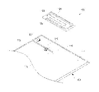
effort has been
continuously exerted to execute functions including control of vehicles,
electric home
appliances, etc., payment of transportation expenses, and a security function
merely
with the mobile communication terminal by mounting a wireless Local Area
Network
(LAN) or Near Field Communication (NFC) function on the mobile communication
terminal, as well as a communication function through communication service
operators. Therefore, the portable terminal represented by the mobile
communication
terminal needs to have various antenna devices mounted thereon. That is, a
mobile
communication service, a wireless LAN, and NFC are made in different frequency
bands, such that respective antenna devices are required.
[4] Moreover, as conversion to a fourth-generation (4G) communication
scheme rep-
resented by wireless bmadband (WiBro) or Long Term Evolution (LTE) has been
made recently, super-high speed and broadband antenna devices are required. As
such,
a plurality of antenna devices are installed in a single portable terminal and
at the same
time, high-performance antenna devices are required. As a super-high speed and
broadband antenna device, an Inverted F Antenna (WA) or a flat-plate WA is
usefully
used.
[5] FIG. 1 is a perspective view schematically showing an antenna device 10
of a
portable terminal according to an embodiment of the conventional art, in which
the
CA 2872492 2018-11-13
81783653
2
ahtenna device 10 is based on an WA structure.
16] The antenna device 10 is structured by forming a radiation
pattern 23 in a carrier 21
mounted on a circuit board 11. The radiation pattern 23 is properly designed
according
to a frequency band and radiation performance required by the portable
terminal, On
an end of the radiation pattern 23 is provided a shortcircuit pin 27 connected
to a
ground layer 13 and is also formed a feeding line 25 with a predeteimin,ed
distance
from the shortcircuit pin 27.
[7] In this IPA structure, when the radiation pattern 23 is positioned on
the ground layer
13, upon application of a transmission/reception signal to the radiation
pattern 23, an
induced current is generated on the ground layer 13 in an inverse direction to
signal
power flowing along the radiation pattern 23. The strength of the inverse
current of the
ground layer 13 increases as the signal power applied to the radiation pattern
23 is
larger and a distance between the ground layer 13 and the radiation pattern 23
is
shorter. The inverse current phenomenon degrades antenna performance,
specifically,
radiation efficiency, and therefore, to suppress the inverse current
phenomenon, it is
desirable to dispose the ground layer 13 and the radiation pattern 23 as far
as possible
from each other.
[8] However, when the antenna device 10 is mounted in the portable
terminal, increasing
the distance between the ground layer 13 and the radiation pattern 23, i.e., a
height H
of the carrier 21 on the circuit board 11 hinders miniaturization of the
portable
terminal.
[9] As an alternative for reducing the height of the carrier in the WA
structure, a fill cut
region 15 is formed by partially removing the ground layer 13 on the circuit
board 11,
and the carrier 21 is disposed in the fill cut region 15. Through such a
structure, the
radiation pattern 23 is disposed in a position out of the ground layer 13 on
the circuit
board 11. By disposing the radiation pattern 23 in the fill cut region 15, the
inverse
current phenomenon is prevented, such that the radiation pattern 23 can be
disposed
closer to the circuit board 11. Tn other words, by forming the fill cut region
15, the
thickness of the antenna device 10 can be reduced. However, it is
substantially im-
possible to mount another part in the fill cut region 15 on the circuit board
11, such that
the use efficiency of the circuit board 11 relative to the area of the circuit
board ills
degraded.
Summary of Invention
Eventually, the IPA structure, in spite of its super-high speed and broadband
per-
[10] formance and usefulness in mounting on the portable terminal, is still
an obstacle to
miniaturization and slimmetization of the portable terminal.
CA 2872492 2018-11-13
81783653
3
[111 To address the above-discussed deficiencies of the prior art, it is a
primary object to
provide an antenna device contributing to miniaturization and slimmerization
of a
portable terminal.
[12] The present application also provides an antenna device that can
efficiently use an
internal space of a portable terminal while being miniaturized and
slimmerized.
[13] According to an aspect of the present application, there is provided
an antenna device
for a portable terminal, the antenna device including a circuit board on a
surface of
which a conductive layer is formed, a slit that removes a portion of the
conductive
layer and extends in a direction, an auxiliary board positioned on the slit to
face a
surface of the circuit board, and a radiation pattern formed on the auxiliary
board, in
which the radiation pattern is disposed to partially enclose the slit.
[14] According to another aspect of the present application, there is
provided an antenna
device for a portable terminal, the antenna device including a circuit board
on a surface
of which a conductive layer is formed, a slit that removes a portion of the
conductive
layer and extends from a side edge of the conductive layer in a direction, an
auxiliary
board positioned on the slit to face a surface of the circuit board, and a
radiation
pattern formed on the auxiliary board, in which the radiation pattern includes
a first
extension portion positioned on the conductive layer in a side of the slit to
extend in
parallel with the slit, a second extension portion extending from an end of
the first
extension portion to enclose an end of the side of the slit, and a third
extension portion
positioned on the conductive layer in the other side of the slit, at least a
portion of
which extending from an end of the second extension portion in parallel with
the slit.
[14a1 According to one aspect of the present invention, there is provided
an antenna device
for a portable terminal, the antenna device comprising: a circuit board
comprising a
conductive layer on a surface thereof; a slit formed by a removal of a portion
of the
conductive layer and configured to extend in a direction, an end of the slit
is opened to
a side edge of the conductive layer and another end of the slit is closed by
another
portion of the conductive layer; a feeding line connected from one side of the
slit
across the slit to the conductive layer in the other side of the slit and
configured to
provide a transmission signal from the one side of the slit to the feeding
line; a
CA 2872492 2018-11-13
81783653
3a
connection terminal installed on the conductive layer in the other side of the
slit; an
auxiliary board positioned on the slit to face the surface of the circuit
board; a
connection pattern provided on a surface of the auxiliary board and arranged
to contact
the connection terminal; and a radiating element formed on the auxiliary board
and
electrically connected with the connection pattern, the radiating element
extends in
parallel with the slit in both sides of the slit and is interconnected in an
outer side of
the closed end of the slit to enclose the slit, wherein a projection of the
radiating
element on the surface of the circuit board is partially positioned on a
circumference of
the slit, without covering the slit, when the antenna device is shown on a
plane view,
and wherein the antenna device generates a current flow on the conductive
layer in the
same direction as that of a signal power flowing on the radiating element.
[1413] According to another aspect of the present invention, there is
provided an antenna
device for a portable terminal, the antenna device comprising: a circuit board
comprising a conductive layer on a surface thereof; a slit which is formed by
removing
a portion of the conductive layer and configured to extend from a side edge of
the
conductive layer in a direction, an end of the slit is opened to a side edge
of the
conductive layer and another end of the slit is closed by another portion of
the
conductive layer; a feeding line connected from one side of the slit across
the slit to the
conductive layer in the other side of the slit and configured to provide a
transmission
signal from the one side of the slit to the feeding line; a connection
terminal installed
on the conductive layer in the other side of the slit; an auxiliary board
positioned on
the slit to face the surface of the circuit board; a connection pattern
provided on a
surface of the auxiliary board and arranged to contact the connection
terminal; and a
radiating element formed on the auxiliary board and electrically connected
with the
connection pattern, wherein the radiating element comprises: a first extension
portion
positioned on the auxiliary board on one side of the slit to extend in
parallel with the
slit; a second extension portion extending from an end of the first extension
portion to
enclose the closed end of the side of the slit; a third extension portion
positioned on the
auxiliary board on the other side of the slit, at least a portion of which
extending from
an end of the second extension portion in parallel with the slit; a fourth
extension
CA 2872492 2018-11-13
81783653
3b
portion extending from an end of the third extension portion and parallel to
the second
extension portion; and a fifth extension portion extending from an end of the
fourth
extension portion and parallel to the first and third extension portions, such
that a
projection of the radiating element on the surface of the circuit board is
partially
positioned on a circumference of the slit, without covering the slit, when the
antenna
device is shown on a plane view.
[15] Before undertaking the DETAILED DESCRIPTION below, it may be
advantageous
to set forth definitions of certain words and phrases used throughout this
patent
document: the terms "include" and "comprise," as well as derivatives thereof,
mean
inclusion without limitation; the term "or," is inclusive, meaning and/or; the
phrases
"associated with" and "associated therewith,' as well as derivatives thereof,
may mean
to include, be included within, interconnect with, contain, be contained
within, connect
to or with, couple to or with, be communicable with, cooperate with,
interleave,
juxtapose, be proximate to, be bound to or with, have, have a property of, or
the like;
and the term ''controller" means any device, system or part thereof that
controls at least
one operation, such a device may be implemented in hardware, firmware or
software,
or some combination of at least two of the same. It should be noted that the
functionality associated with any particular controller may be centralized or
distributed, whether locally or remotely. Definitions for certain words and
phrases are
provided throughout this patent document, those of ordinary skill in the art
should
understand
CA 2872492 2018-11-13
81783653
4
that in many, if not most instances, such definitions apply to prior, as well
as future
uses of such defined words and phrases.
[16] The antenna device for the portable terminal structured as described
above can
control induced current generated around the slit in the same direction as
signal power
of the radiation pattern even when the radiation pattern is disposed on the
conductive
layer. Therefore, even when the radiation pattern is disposed on the
conductive layer, it
can prevent radiation performance from being degraded by an inverse current
phenomenon. Moreover, by preventing the inverse current phenomenon, a total
height
of the antenna device can be reduced even if the conductive layer is removed
from the
region of the circuit board in which the radiation pattern is disposed,
contributing to
reduction of the thickness of the portable terminal, Furthermore, in
implementation of
the inverse F antenna structure or a flat-plate inverse F antenna structure,
the fill cut
region does not need to be formed, thereby further securing an area on which a
part
such as an integrated circuit chip can be mounted on the circuit board,
Brief Description of Drawings
[17] For a more complete undentanding of the present disclosure and its
advantages,
reference is now made to the following description taken in conjunction with
the ac-
companying drawings, in which like reference numerals represent like parts:
[18] FIG. 1 is a perspective view schematically showing an antenna device
of a portable
terminal;
1191 FIG. 2 is perspective view showing an antenna device of a
portable terminal
according to embodiments of the present disclosure;
[201 FIG. 3 is a plane view showing an antenna device shown in FIG, 2;
[21] FIG. 4 is a plane view showing a bottom surface of an auxiliary board
of an antenna
device shown in FIG. 2;
[22] FIG. 5 is a plane view showing a state in which an auxiliary board is
removed from
an antenna device shown in FIG. 3;
[23] FIG. 6 is a side view showing a modified example of an antenna device
shown in
FIG. 2;
[24] FIG. 7 is a view for describing an induced current flow on a
conductive layer in an
antenna device shown in FIG. 2;
[25] FIG. 8 is a view for describing another modified example of an antenna
device
shown in FIG. 2;
[26] PIGs. 9 and 10 illustrate an implementation of an antenna device shown
in FIG. 2;
[27] FIG. 11 is a view showing a result of measurement of a radiation
efficiency of an
antenna device shown in FIG. 10; and
CA 2872492 2018-11-13
81783653
[28) FIG. 12 is a view showing a result of measurement of a reflection
coefficient of an
antenna device shown in FIG. 10,
Detailed Description of the Preferred Embodiments
[29] FIGURES 2 through 12, discussed below, and the various embodiments
used to
describe the principles of the present disclosure in this patent document are
by way of
illustration only and should not be construed in any way to limit the scope of
the
disclosure. Those skilled in the art will understand that the principles of
the present
disclosure may be implemented in any suitably arranged wireless communications
device. Hereinafter, an exemplary embodiment of the present invention will be
described in detail with reference to the accompanying drawings. Herein, a
detailed de-
scription of well-known structures will not be provided if it unnecessarily
obscures the
subject matter of the present invention.
[30] As shown in FIGs. 2 through 7, an antenna device 100 for a portable
terminal
according to an embodiment of the present disclosure includes a circuit board
101 on
which a conductive layer 111 is formed and an auxiliary board 121 on which a
radiation pattern 123 is formed. The radiation pattern 123 is disposed to
partially
enclose a slit 113 formed by removing a part of the conductive layer 111.
[31] On the circuit board 101 are mounted a communication circuit for
transmitting and
receiving a signal through the antenna device 100 and various circuit devices
for con-
trolling operations of the portable terminal or storing information. On a
surface of the
circuit board 101 is provided the conductive layer Ill to provide a ground of
circuit
devices provided on the circuit board 101. That is, the circuit board 101 is
used as the
main circuit board 101 of the portable terminal.
[32] As mentioned previously, the slit 113 is formed by removing a part of
the conductive
layer 111, and extends in a direction on the circuit board 101. Preferably, an
end of the
slit 113 is opened to the edge of the conductive layer 111 and the other end
thereof is
positioned in the conductive layer 111 and thus is closed. Moreover, the slit
113
extends in parallel with a corner of the circuit board 101 in a position
adjacent to the
comer of the circuit board 101.
[33] The auxiliary board 121 is disposed on the slit 113 while facing the
circuit board 101.
When viewed from the plane view shown in FIG. 3, the slit 113 is covered by
the
auxiliary board 121. The auxiliary board 121 can be manufactured with a
synthetic
resin material or a dielectric used to manufacture a typical circuit board.
[34] The radiation pattern 123 can be formed by processing a printed
circuit pattern or a
metal thin plate and disposing it on a surface of the auxiliary board 121. The
printed
circuit pattern can be formed directly on the auxiliary board 121 through
processing
such as plating/etching or the like, or can be used as the radiation pattern
123 by
CA 2872492 2018-11-13
6
CA 02872492 2014-11-03
WO 2013/180341 PCT/ICR2012/007281
attaching a flexible printed circuit board thereto. The radiation pattern
using the metal
thin plate is formed by cutting a metal material, e.g., a thin plate of
copper, and
attaching the cut metal material to the auxiliary board 121. The radiation
pattern 123
preferably extends to partially, more specifically, partially enclose each of
at least a
side, the other end, and the other side of the slit 113.
[35] In certain embodiments of the present disclosure, the radiation
pattern 123 includes a
first extension portion 123a, a second extension portion 123b, and a third
extension
portion 123c. The first extension portion 123a is positioned on the conductive
layer
111 in the side of the slit 113 and extends in parallel with the slit 113, and
the second
extension portion 123b extends from an end of the first extension portion 123a
to
enclose the other end of the slit 113, i.e., the closed end of the slit 113.
As shown in
FIG. 3, the second extension portion 123b can overlap at a portion thereof
with the
other end of the slit 113. The third extension portion 123c extends in at
least a portion
thereof from the end of the second extension portion 123b in parallel with the
slit 113,
and is positioned on the conductive layer 111 in the other side of the slit
113.
[36] That is, the radiation pattern 123 extends from both sides of the slit
113 in parallel,
and is interconnected in an outer side of the other end of the slit 113. The
third
extension portion 123c can have a free pattern after extending by a
predetermined
length from the end of the second extension portion 123b in parallel with the
slit 113.
The partial free pattern of the third extension portion 123c can be adjusted
to optimize
a frequency band in which the antenna device 100 operates, radiation
efficiency, and
so forth.
[37] In the foregoing description of the radiation pattern 123, 'the
radiation pattern 123 is
formed or disposed to enclose the slit 113' does not mean that the radiation
pattern 123
is actually positioned on the circumference of the slit 113 in the same height
as the slit
113. That is, the slit 113 is formed on the conductive layer 111 and the
radiation
pattern 123 is formed on the auxiliary board 121 disposed to face the
conductive layer
111, such that in practice, the radiation pattern 123 and the slit 113 are
positioned in
different heights with respect to the circuit board 101. However, as shown in
FIG. 3,
when the antenna device 100 is shown on the plane view, the radiation pattern
123 po-
sitioned around the slit 113 is described as 'being formed or disposed to
enclose the slit
113'.
[38] In the antenna device 100 structured as described above, induced
current is generated
on the conductive layer 111 by signal power flowing on the radiation pattern
123, but
according to a structure which applies a signal to the radiation pattern 123,
current
flow on the conductive layer 111 can be induced. That is, the flow of current
is
generated on the conductive layer 111 in the same direction as that of signal
power
flowing on the radiation pattern 123, thereby suppressing an inverse current
7
CA 02872492 2014-11-03
WO 2013/180341 PCT/ICR2012/007281
phenomenon. Such suppression can be possible by using some region in the other
side
of the slit 113, i.e., a region of the conductive layer 111 in which the third
extension
portion 123c is positioned as the radiation pattern 123. In certain
embodiments of the
present disclosure, for brevity, a pattern formed on the auxiliary board 121
is referred
to as the radiation pattern 123, but the antenna device 100 also uses a
portion of the
conductive layer 111 as a radiation element.
[39] Referring to FIG. 5, the antenna device 100 includes a feeding line
115 that is
connected from a side 113a of the slit 113 across the slit 113 to the
conductive layer
111 in the other side of the slit 113. The antenna device 100 also includes a
connection
terminal 117 installed on the conductive layer 111 in a position adjacent to
an open end
of the slit 113. The connection terminal 117 is formed by processing a leaf
spring, and
is fixed on the conductive layer 111 while being electrically connected to the
conductive layer 111. The connection terminal 117 contacts a connection
pattern 125
formed on the other surface of the auxiliary board 121 to be electrically
connected with
the radiation pattern 123. As shown in FIGs. 3 and 4, the connection pattern
125
extends from the other surface of the auxiliary board 121 to enclose a side of
the
auxiliary board 121, such that the connection pattern 125 is connected to the
radiation
pattern 123 on the other surface of the auxiliary board 121. The connection
pattern 125
is formed only on the other surface of the auxiliary board 121, and as shown
in FIG. 6,
the connection pattern 125 can be electrically connected to the radiation
pattern 123
through a via hole 127 formed to penetrate the auxiliary board 121.
[40] For impedance matching, the antenna device 100 can include an
impedance matching
element 119 that can be disposed across the slit 113 or on the feeding line
115.
Impedance matching of the antenna device 100 can be achieved by adjusting a
distance
(d of FIG. 5) from the end of the slit to the feeding line 115.
[41] To the antenna device 100 can be applied a transmission signal through
the feeding
line 115. The transmission signal applied to the feeding line 115 goes to the
radiation
pattern 123 through some region of the other side of the slit 113, indicated
as '113b',
and the connection terminal 117. In this case, a region 113c that connects the
region
113b of the conductive layer 111 used as the radiation pattern 123 in the
other side of
the slit 113 to the conductive layer 111 in the side of the slit 113 is used
as a
shortcircuit pin. Eventually, the region 113b of the conductive layer 111 in
the other
side of the slit 113 is used together with the radiation pattern 123 as a
radiation element
of the antenna device 100.
[42] In this state, upon application of the transmission signal to the
feeding line 115,
current flow f is formed around the slit 113. The current flow f follows a
counter-
clockwise direction around the slit 113 as shown in FIG. 7. According to the
transmission signal applied to the feeding line 115, signal power flowing on
the
8
CA 02872492 2014-11-03
WO 2013/180341 PCT/ICR2012/007281
radiation pattern 123 also follows the counterclockwise direction around the
slit 113,
such that the current flow around the slit 113 and the flow of signal power of
the
radiation pattern 123 also follow the same direction.
[43] As such, the antenna device 100 according to the present disclosure
forms the slit
113 on the conductive layer 111, which provides the ground on the circuit
board 101,
and uses a region of the conductive layer 111 as a radiation element of the
antenna
device 100. In signal transmission/reception operations, the flow of current
induced on
the conductive layer 111 is controlled to prevent an inverse current
phenomenon. In
certain embodiments of the present disclosure, by using disposition of the
feeding line
115 and the connection terminal 117, the flow f of current induced on the
conductive
layer 111 is controlled to follow the counterclockwise direction around the
slit 113.
Such control has to be performed in a direction in which the radiation pattern
123
extends on the circumference of the slit 113, more specifically, in the
direction of the
signal power flowing on the radiation pattern 123.
144] In this way, the antenna device 100 according to the present
disclosure forms the slit
113 on the conductive layer 111 that provides the ground, thereby controlling
the flow
f of the current flowing around the slit 113, such that the radiation pattern
123 can be
disposed in adjacent to the conductive layer 111. Therefore, stable antenna
per-
formance can be secured and at the same time, the radiation pattern 123 and
the
conductive layer 111 can be disposed in adjacent to each other. That is, when
compared to in a conventional inverse F antenna, a distance h between the
conductive
layer 111, which provides the ground, and the radiation pattern 123 can be
reduced. In
case of a built-in antenna applied to a conventional portable terminal, to
secure stable
antenna performance, an interval of at least 5mm needs to be maintained
between the
ground layer 11 and the radiation pattern 23. Alternatively, the antenna
device 100
according to the present disclosure can secure performance equal to or higher
than a
conventional antenna device even when the radiation pattern 123 is formed
within an
interval of 2mm or less from the conductive layer 111.
[45] In addition, conventionally, when a built-in antenna such as an
inverse F antenna is
disposed, to secure antenna performance, a fill cut region needs to be formed
by
partially removing the ground layer, but the region 113b of the conductive
layer 111
used as a radiation element can still provide the ground. That is, in a high-
frequency
band in which the antenna device 100 operates, the region 113b of the
conductive layer
111 is used as a part of the radiation element, but the region 113b of the
conductive
layer 111 can still provide the ground for some electric parts or assembly
engagement
members operating in a low-frequency band. Accordingly, when compared to a con-
ventional built-in antenna, the antenna device 100 according to the present
disclosure
can easily reduce its thickness and improve the use efficiency of the circuit
board 101.
9
CA 02872492 2014-11-03
WO 2013/180341 PCT/ICR2012/007281
[461 The operating frequency of the antenna device 100 can be adjusted
according to a
width s of the slit 113 or a width or shape of the radiation pattern 123.
Moreover, a
lumped circuit element, etc., can be disposed on the radiation pattern 123 or
the slit
113 to adjust the operating frequency or the frequency bandwidth. As shown in
FIG. 8,
another slit 213 can be formed on the region 113b of the conductive layer 111
in the
other side of the slit 113, or the antenna device 100 can be manufactured as a
multi-
band antenna according to the shape of the radiation pattern 123.
[471 According to the structure shown in FIGs. 2 and 3, a slit having a
length of 20mm is
formed in parallel with a corner of a circuit board without a distance of 5mm
from the
corner of the circuit board, thereby implementing the antenna device 100.
Referring to
FIG. 6 further, a distance between the conductive layer 111 and the radiation
pattern
123 is 1.4mm, and a thickness of the auxiliary board 121 is 0.4mm. A state
where the
antenna device 100 is implemented is illustrated in FIGs. 9 and 10. For the
above-
manufactured antenna device, results of measurement of a radiation efficiency
(RE)
and a total radiation efficiency (TRE) of the manufactured antenna device are
shown in
FIG. 11, and a reflection coefficient is shown in FIG. 12. It can be seen from
FIGs. 11
and 12 that the antenna device actually implemented according to the present
disclosure can secure stable operating characteristics in a band of 700 ¨
800MHz and a
band of 1.8 ¨ 2.2GHz.
[48] Although the present disclosure has been described with an exemplary
embodiment,
various changes and modifications may be suggested to one skilled in the art.
It is
intended that the present disclosure encompass such changes and modifications
as fall
within the scope of the appended claims.