Note: Descriptions are shown in the official language in which they were submitted.
CA 02872753 2014-11-05
WO 2014/011243 PCT/US2013/032927
- 1 -
LOAD BUSS ASSEMBLY
AND METHOD OF MANUFACTURING THE SAME
CROSS REFERENCE TO RELATED APPLICATION
This application claims the benefit of U.S. Provisional Patent
Application Serial No. 61/670,741, filed July 12, 2012, which is incorporated
by
reference herein.
BACKGROUND
Field
The disclosed concept pertains generally to load modules and, more
particularly, to load buss assemblies for such load modules. The disclosed
concept
further pertains to methods of manufacturing load buss assemblies.
Background Information
U.S. Patent No. 8,094,436 discloses a plug-in circuit breaker panel
including a housing, an electrical bus structure coupled to the housing, and a
number
of first plug-in members coupled to the electrical bus structure. A number of
circuit
breakers include a first surface and a second plug-in member disposed opposite
the
first surface. The second plug-in member of each of the number of circuit
breakers is
mated with a corresponding one of the number of first plug-in members. A plate
member is removably coupled to the housing. The plate member includes a first
surface and an opposite second surface. The first surface of the number of
circuit
breakers engages the opposite second surface of the plate member in order to
maintain
mating of each of the number of circuit breakers with the corresponding one of
the
number of first plug-in members.
The rear of the plug-in circuit breaker panel includes first and second
feeders for a three-phase alternating current (AC) system. Typically, for each
of the
feeders, there can be a single three-pole AC circuit breaker and a plurality
of single
pole AC circuit breakers for each of the three phases. For example, each of
the
feeders is a three-terminal terminal block having three power terminals for
the three
phases of the corresponding feeder. A first surface of the electrical bus
structure is
proximate the number of first plug-in members, and the feeders and power
terminals
thereof are coupled to the opposite second surface along with a number of load
connectors. The load connectors include load outputs (e.g., loads) from the
CA 02872753 2014-11-05
WO 2014/011243 PCT/US2013/032927
- 2 -
corresponding circuit breakers associated with the respective feeders. In a
similar
manner, the power inputs (e.g., lines) to the corresponding circuit breakers
are
associated with the respective feeders. The electrical bus structure (e.g., a
number of
inner power layers thereof) suitably routes the load outputs from and the
power inputs
to the various circuit breakers.
While the feeders are directly coupled to the electrical bus structure at
corresponding terminal blocks and power terminals thereof, the load outputs
from the
circuit breakers are electrically connected between the electrical bus
structure and
corresponding load connectors by a number of discrete conductors or ribbon
cable.
As a result, a manual operation is needed to electrically connect the load
outputs
between the electrical bus structure and the corresponding load connectors.
Also, the
load connectors and the discrete conductors or ribbon cable significantly
increase the
size of the plug-in circuit breaker panel.
Therefore, there is room for improvement in circuit breaker panels.
There is also room for improvement in load buss assemblies of circuit
breaker panels.
There is further room for improvement in methods of manufacturing
load buss assemblies of circuit breaker panels.
SUMMARY
These needs and others are met by aspects of the disclosed concept
which place a plurality of load conductors within a thermally conductive
substrate;
place a portion of a load connector within the thermally conductive substrate;
and
electrically connect the load conductors to the portion of the load connector
within the
thermally conductive substrate.
In accordance with one aspect of the disclosed concept, a load buss
array assembly comprises: a thermally conductive substrate; a plurality of
load
conductors placed within the thermally conductive substrate; and a portion of
a load
connector placed within the thermally conductive substrate, wherein the load
conductors are electrically connected the portion of the load connector within
the
thermally conductive substrate.
In accordance with another aspect of the disclosed concept, a method
of manufacturing a load buss array assembly comprises: placing a plurality of
load
CA 02872753 2014-11-05
WO 2014/011243
PCT/US2013/032927
- 3 -
conductors within a thermally conductive substrate; placing a portion of a
load
connector within the thermally conductive substrate; and electrically
connecting the
load conductors to the portion of the load connector within the thermally
conductive
substrate.
BRIEF DESCRIPTION OF THE DRAWINGS
A full understanding of the disclosed concept can be gained from the
following description of the preferred embodiments when read in conjunction
with the
accompanying drawings in which:
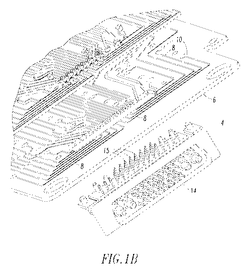
Figure lA is an isometric view of a plurality of miniature conductive
traces for a load buss array assembly in accordance with embodiments of the
disclosed
concept.
Figure 1B is an exploded isometric view of the miniature conductive
traces of Figure 1A, a thermally conductive substrate and a load connector for
a load
buss array assembly in accordance with another embodiment of the disclosed
concept.
Figure 1C is an isometric view of the miniature conductive traces and the
load connector of Figure 1B.
Figures 2A and 2B are an isometric view and a side vertical elevation
view, respectively, showing the load conductive traces of a load buss array
assembly of a
load module assembly in accordance with another embodiment of the disclosed
concept.
Figures 3A and 3B are an isometric view and a side vertical elevation
view, respectively, of a circuit breaker panel including the load module
assembly with
embedded feeder layers and the load buss array assembly of Figure 2A.
Figure 4 is a plan view of the circuit breaker panel of Figure 3A with a
cover removed to show a load connector.
Figures 5A and 5B are an isometric view and a side vertical elevation
view, respectively, of a backplane module including the embedded feeder layers
and the
load buss array assembly of Figure 2A.
Figure 6 is a plan view of the embedded feeder layers of the backplane
module of Figure 5A with the load buss array assembly removed.
DESCRIPTION OF THE PREFERRED EMBODIMENTS
As employed herein, the term "number" shall mean one or an integer
greater than one (i.e., a plurality).
CA 02872753 2014-11-05
WO 2014/011243 PCT/US2013/032927
- 4 -
As employed herein, the statement that two or more parts are
"connected" or "coupled" together shall mean that the parts are joined
together either
directly or joined through one or more intermediate parts. Further, as
employed
herein, the statement that two or more parts are "attached" shall mean that
the parts
are joined together directly.
The disclosed concept employs miniature conductive traces embedded
in a thermally conductive substrate as part of a method of construction and
automated
electrical connection of a load connector to a plurality of load buss array
miniature
conductive traces. This method simplifies the construction of a load module,
and
provides considerable size, depth and weight benefits as compared to known
methods
of packaging a wiring interconnect.
The disclosed concept preferably provides: (1) a 100% thermally
conductive backplane; and (2) a 100% embedded load conductor solution.
The materials of the miniature conductive traces can be, for example,
copper or aluminum.
The materials of the thermally conductive substrate can be relatively
highly heat-resistant resins like a liquid-crystal polymer (LCP) or
polyetheretherketone (PEEK).
The disclosed concept is described in association with subminiature or
aircraft circuit breakers, although the disclosed concept is applicable to a
wide range
of different circuit breakers for a wide range of different applications. Such
circuit
breakers can be employed, for example and without limitation, in aircraft
alternating
current (AC) systems having a typical frequency of about 400 Hz, but can also
be
used in direct current (DC) systems. It will also become evident that the
disclosed
concept is applicable to other types of circuit breaker panels including those
used in
AC systems operating at other frequencies; to larger circuit breakers, such as
miniature residential or commercial circuit breakers; and to a wide range of
circuit
breaker applications, such as, for example, residential, commercial,
industrial,
aerospace, and automotive. As further non-limiting examples, both AC (e.g.,
without
limitation, 120, 220, 480-600 VAC) operation at a wide range of frequencies
(e.g.,
without limitation, 50, 60, 120, 400 Hz, and higher or lower frequencies) and
DC
operation (e.g., without limitation, 42 VDC) are possible. As still further
non-limiting
CA 02872753 2014-11-05
WO 2014/011243 PCT/US2013/032927
- 5 -
examples, single phase and plural phase (e.g., without limitation, three
phase)
operation are possible.
The miniature conductive traces 2 of a load buss array assembly 4
(Figures 1B and 1C) are suitably embedded in a thermally conductive substrate
6
(Figure 1B). For example and without limitation, the thermally conductive
substrate 6
is suitably molded or machined to have grooves 8 and holes 10 to accept the
miniature
conductive traces 2 as shown in Figure 1B. The corresponding load module 12
(Figures 2A and 2B) replaces a known prior load module (not shown) having
discrete
wiring over-molded into urethane and attached to an embedded feed section via
sockets. See, for example, U.S. Patent No. 8,094,436, which is incorporated by
reference herein.
The disclosed method simplifies the construction of the load buss array
assembly 4 and, thus, the load module 12. This permits, for example, the
miniature
conductive traces 2, which function as load conductors, to be embedded in the
molded
thermally conductive substrate 6 (e.g., without limitation, a liquid-crystal
polymer
(LCP), such as CoolPoly E-series thermally conductive plastic marketed by
Cool
Polymers, Inc. of North Kingstown, Rhode Island; a suitable thermally
conductive
and electrically insulative epoxy), which seals and insulates the load
conductors.
Alternatively, if the thermally conductive substrate 6 is machined, then
the load conductors can be sealed and insulated (e.g., a conductor is placed
in a
channel and is sealed and insulated from other conductors and from the outside
environment) by employing a suitable sealant (not shown) such as, for example
and
without limitation, tape, glue or epoxy. For example, the material is
electrically
insulative with adhesive on both sides, and is relatively very thin (e.g.,
without
limitation, 0.005 in.) and conforms to the substrate 6 and traces 2.
The miniature conductive traces 2 can be automatically coupled to a
load connector 14 and its load pins 15 (Figures 1B and 1C) by fixturing and by
employing a conventional wave soldering process. For example, the load
conductors
are placed in the thermally conductive substrate 6 during molding, and the
load
connector 14 is fixtured to have a precise location and fit. Then, the load
buss array
assembly 4 is fed through a suitable wave soldering station (not shown) to
electrically
couple the connector load pins 15 and the load connector 14 to the load
conductor
CA 02872753 2014-11-05
WO 2014/011243 PCT/US2013/032927
- 6 -
traces 2. Alternatively, this could be a manual operation, but would not be
cost
favorable. This eliminates point-to-point wiring attachments (e.g., without
limitation,
crimps; hand soldering). The disclosed concept adds about another 0.25" of
depth for
the load thermally conductive substrate layers 16, which are directly coupled
to feeder
layers 18 of the load module 12 (Figures 2A, 2B, 3A and 3B). Also, a
significant
overall depth reduction to about 1" to about 2" from about 4" to about 5" of
baseline
depth is provided for the corresponding circuit breaker panel 20 (Figures 3A,
3B and
4).
Figure 4 shows the circuit breaker panel 20 with its cover 22 (shown in
Figures 3A and 3B) removed to show the load connector 14.
Figures 5A and 5B show the backplane module 24 of the circuit
breaker panel 20.
Various possible methods to place the load conductors within the
thermally conductive substrate 6 include: (1) over-molding the miniature
conductive
traces 2 into the thermally conductive substrate 6; (2) hand placement of the
miniature
conductive traces 2 into the thermally conductive substrate 6; and (3)
automated
bobbin winding placement if the miniature conductive traces 6 have a suitable
cross-
section (e.g., without limitation, flat; round; square). For example, for the
latter
method, an uncoated load conductor (not shown) is placed with a CNC (x,y,z)
controlled winder (not shown), such that a placed wire conductor (e.g., 2 of
Figure
2A) is cut and placed without the use of manual touch-labor. The automated
winding
placement is suited to high-volume production, much like a wire feeder. This
precisely feeds a wire cut length (not shown) to a nozzle (not shown), which
is CNC-
controlled to place the conductor (e.g., 2 of Figure 1A) into a groove 8
(Figure 1B) in
the thermally conductive substrate 6 (Figure 1B).
While specific embodiments of the disclosed concept have been
described in detail, it will be appreciated by those skilled in the art that
various
modifications and alternatives to those details could be developed in light of
the
overall teachings of the disclosure. Accordingly, the particular arrangements
disclosed are meant to be illustrative only and not limiting as to the scope
of the
disclosed concept which is to be given the full breadth of the claims appended
and
any and all equivalents thereof.