Note: Descriptions are shown in the official language in which they were submitted.
- 1 -
BEAM IMAGING SENSOR
[0001] Not applicable.
[0002]
RELATED APPLICATION DATA
[0003] This patent application claims priority to United States
Provisional
Patent Application No. 61/646,627 filed May 14, 2012 and titled "Beam Imaging
Sensor."
FIELD AND BACKGROUND OF THE INVENTION
1. Field of the Invention
[0004] The present invention relates generally to the field of sensors
for beam
imaging and, in particular, to a new and useful beam imaging sensor for use in
determining, for example, the power density distribution of a beam including,
but not
limited to, an electron beam or an ion beam. In one embodiment, the beam
imaging
sensor of the present invention comprises, among other items, a
circumferential slit
that is either circular, elliptical or polygonal in nature.
2. Description of the Related Art
[0005] Electron beams are considered to be the most precise and clean
method available for welding thick sections of materials. Unfortunately,
electron
beams suffer one critical deficiency, namely the repeatability of focusing the
beam to
a known power density. Without the ability to reliably reproduce the power
distribution in an electron beam, weld quality cannot be guaranteed. This
problem is
exacerbated by the fact the many welds are made over a period of time and with
different welding operators. Further complications arise when welds are
developed
on one machine than transferred to a different machine for production. Various
electron beam diagnostic methods have been developed that, at some level,
enable
the characterization of the power density distribution in high power electron
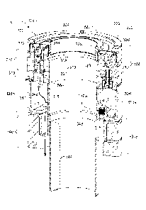
beams.
CA 2873398 2019-08-26
CA 02873398 2014-11-12
WO 2013/173322 PCT/US2013/040928
- 2 -
Such diagnostic methods are exemplified by United States Patent Nos.
5,382,895;
5,468,966; 5,554,926; 5,583,427; 6,300,755; 7,288,772; 7,348,568; 7,378,830;
and
7,902,503. However, the methods and sensors disclosed therein all suffer from
a
number of drawbacks. While not wishing to be bound to any one drawback, some,
if
not all, of the prior art sensors suffer from thermal load drawbacks that
cause the
sensors of the prior art to fail at lower energy levels (e.g., 5 kW).
[0006] Given the above, a need exists for a beam imaging sensor that
provides superior functionality and accuracy while still being able to
withstand beam
energy settings in excess of 5 kW.
SUMMARY OF THE INVENTION
[0007] The present invention relates generally to the field of sensors for
beam
imaging and, in particular, to a new and useful beam imaging sensor for use in
determining, for example, the power density distribution of a beam including,
but not
limited to, an electron beam or an ion beam. In one embodiment, the beam
imaging
sensor of the present invention comprises, among other items, a
circumferential slit
that is either circular, elliptical or polygonal in nature.
[0008] Accordingly, one aspect of the present invention is drawn to a beam
imaging sensor comprising: a cylindrically-shaped sensor body, wherein the
sensor
body has a top end and a bottom end, the top end having at least one channel
formed therein; a Faraday cup located within the at least one channel, the
Faraday
cup being positioned to receive at least a portion of an electron, or ion,
beam; an
inner slit disc and an outer slit disc positioned at the top end of the least
one channel
so as to be positioned above the Faraday cup, the inner and outer slit discs
being
able to nest together to form a slit there between and where the slit so
formed
permits the passage of at least a portion of an electron, or ion, beam to the
Faraday
cup located there below; and at least one conductive lead in electrical
communication with the Faraday cup, the at least one conductive lead being
able to
conduct an electrical signal generated by the portion of the beam that comes
into
contact with the Faraday cup.
[0009] In yet another aspect of the present invention, there is provided a
beam
imaging sensor comprising: a cylindrically-shaped sensor body, wherein the
sensor
body has a top end and a bottom end, the top end having at least one channel
CA 02873398 2014-11-12
WO 2013/173322 PCT/US2013/040928
- 3 -
formed therein; a cylindrically-shaped electronics enclosure, wherein the
electronics
enclosure has a top end and a bottom end, the top end of the electronics
enclosure
being coupled to the bottom end of the sensor body; a Faraday cup located
within
the at least one channel, the Faraday cup being positioned to receive at least
a
portion of an electron, or ion, beam; an inner slit disc and an outer slit
disc positioned
at the top end of the least one channel so as to be positioned above the
Faraday
cup, the inner and outer slit discs being able to nest together to form a slit
there
between and where the slit so formed permits the passage of at least a portion
of an
electron, or ion, beam to the Faraday cup located there below; and at least
one
conductive lead in electrical communication with the Faraday cup, the at least
one
conductive lead being able to conduct an electrical signal generated by the
portion of
the beam that comes into contact with the Faraday cup.
[0010] In yet another aspect of the present invention, there is provided a
beam
imaging sensor comprising: a cylindrically-shaped sensor body, wherein the
sensor
body has a top end and a bottom end, the top end having at least one channel
formed therein; a cylindrically-shaped electronics enclosure, wherein the
electronics
enclosure has a top end and a bottom end, the top end of the electronics
enclosure
being coupled to the bottom end of the sensor body; a cylindrically-shaped
clamp
ring body and a cylindrically-shaped lower clamp ring, wherein the clamp ring
body
and the clamp ring are coupled to one another and together have a top end and
a
bottom end, the top end of the coupled structure being coupled to the bottom
end of
the electronics enclosure; a Faraday cup located within the at least one
channel, the
Faraday cup being positioned to receive at least a portion of an electron, or
ion,
beam; an inner slit disc and an outer slit disc positioned at the top end of
the least
one channel so as to be positioned above the Faraday cup, the inner and outer
slit
discs being able to nest together to form a slit there between and where the
slit so
formed permits the passage of at least a portion of an electron, or ion, beam
to the
Faraday cup located there below; and at least one conductive lead in
electrical
communication with the Faraday cup, the at least one conductive lead being
able to
conduct an electrical signal generated by the portion of the beam that comes
into
contact with the Faraday cup.
[0011] In yet another aspect of the present invention, there is provided a
beam
imaging sensor as shown and described herein, and/or a beam imaging sensor as
CA 02873398 2014-11-12
WO 2013/173322 PCT/US2013/040928
- 4 -
shown and described in any of the Figures attached hereto. In still another
aspect of
the present invention, there is provided a method of utilizing a beam imaging
sensor
as shown and described herein.
[0012] The various features of novelty which characterize the invention are
pointed out with particularity in the claims annexed to and forming a part of
this
disclosure. For a better understanding of the invention, its operating
advantages and
specific benefits attained by its uses, reference is made to the accompanying
drawings and descriptive matter in which exemplary embodiments of the
invention
are illustrated.
BRIEF DESCRIPTION OF THE DRAWINGS
[0013] Figure 1 is a partial cut-away illustration of a beam imaging sensor
of
the prior art;
[0014] Figure 2 is a partial cut-away illustration of a beam imaging sensor
according to one embodiment of the present invention;
[0015] Figure 3 is a partial close-up illustration of the top portion of
the beam
imaging sensor of Figure 2;
[0016] Figure 4 is a partial top-down illustration of a beam imaging sensor
according to another embodiment of the present invention;
[0017] Figure 5 is a partial top-down illustration of a beam imaging sensor
according to still another embodiment of the present invention; and
[0018] Figure 6 is a close up illustration of a beam imaging sensor of the
present invention containing a detailed illustration of the beam path through
the
sensor;
[0019] Figure 7 is a close-up illustration of the MFC portion of a beam
imaging
sensor according to the present invention;
[0020] Figure 8 is a close-up illustration of the MFC portion of a beam
imaging
sensor illustrating one possible design layout for the MFC portion of a beam
imaging
sensor according to one embodiment of the present invention;
[0021] Figure 9 is a close-up illustration of a side portion of beam sensor
300
illustrating an alternative attachment means for securing outer clamp ring 322
to
sensor body 302;
CA 02873398 2014-11-12
WO 2013/173322 PCT/US2013/040928
- 5 -
[0022] Figure 10 is a close-up illustration of a side portion of beam
sensor 300
illustrating another alternative attachment means for securing outer clamp
ring 322 to
sensor body 302;
[0023] Figure 11 is a close-up cut away illustration of beam sensor 300
illustrating one possible attachment means for securing one or more clamp arms
to
sensor body 302 so as to facilitate securing outer clamp ring 322 to sensor
body
302;
[0024] Figure 12 is a close-up illustration of a portion of beam sensor
300
illustrating an alternative attachment means for securing inner clamp ring 320
to
sensor body 302;
[0025] Figure 13 is a partial top-down illustration of a portion of a beam
imaging sensor according to still another embodiment of the present invention;
and
[0026] Figure 14 is a partial top-down illustration of a portion of a beam
imaging sensor according to still yet another embodiment of the present
invention;
and
[0027] Figures 15 through 17 are partial illustration of another set of
nesting
slit discs according to still yet another embodiment of the present invention.
DESCRIPTION OF THE INVENTION
[0028] While the present invention will be described in terms of an
electron
beam, or ion beam, the present invention is not limited thereto. Rather, the
beam
imaging sensor of the present invention can be utilized in any situation where
one
wants to ascertain the power density distribution of a beam of energy.
[0029] As noted above, the present invention relates generally to the
field of
sensors for beam imaging and, in particular, to a new and useful beam imaging
sensor for use in determining, for example, the power density distribution of
a beam
including, but not limited to, an electron beam or an ion beam. In one
embodiment,
the beam imaging sensor of the present invention comprises, among other items,
a
circumferential slit that is either circular, elliptical or polygonal (be it a
regular polygon
or an irregular polygon) in nature. As utilized herein the word
"circumferential"
denotes the location and/or positioning of the slit in the present invention
relative
various other parts of the beam imaging sensor. The word "circumferential"
does not
CA 02873398 2014-11-12
WO 2013/173322 PCT/US2013/040928
- 6 -
however limit the geometrical shape of the slit in the beam imaging sensor of
the
present invention.
[0030] Turning
to Figure 1, Figure 1 is an illustration of a prior art beam
imaging sensor 102 having a modified Faraday cup (MFC). As can be seen in
Figure 1, the modified Faraday cup (MFC) imaging sensor 102 is subjected to a
high
power beam 111. As illustrated in Figure 1, MFC sensor 102 includes a slit
disk
assembly 201, a conducting disk 203 located below the slit disk assembly 201,
a
Faraday cup assembly 206 located below the conducting disk 203, and a start-
stop
target 214 located proximate the slit disk assembly 201. A
multiplicity of
circumferential radial slits 216 and a trigger probe 117 are located in the
slit disk
assembly 201. A desired number of circumferential radial slits 212 are located
in the
conducting disk 203. In order to keep the MFC sensor 102 from over-heating
during
use, a heat sink is placed in close proximity to the components. An active
cooling
system, using water or other cooling fluid, can be further integrated into the
heat
sink.
[0031] When
utilized in a diagnostic system as known to those of skill in the
art, sensor 102 provides a manner by which to measure the power density
distribution of a high power and high intensity electron, or ion, beam 111.
During
operation, the beam 111 is rotated about the central point of the slit disk
assembly
201 over the aligned radial slits 216 and 212. Electrons or ions pass through
the
aligned radial slits 216 and 212 and are intercepted by the Faraday cup
assembly
206 where they are detected and a signal is sent to the measuring and data
acquisition system to measure the profile of the beam. Computed tomography can
then be used to reconstruct the power density distribution of the beam 111.
[0032] In order
to prevent damage to the tungsten slit disk assembly 201, the
time over which the beam 111 comes in contact with the tungsten slit disk
assembly
201 is reduced. In order to do this, the target block 214 is located to the
side of the
tungsten slit disk assembly 201. The target block 214 is made of a refractory
metal.
The beam 111 is first directed onto the target block 214 as illustrated in
Figure 1, and
then the beam is translated to the radial slits 216, where it is translated in
a circle
indicated at 111a for a minimum number of rotations and then translated back
onto
the target block 214. The trigger probe 117 initiates the overall measuring
system
(not pictured). This is accomplished by trigger probe 117 sensing scattered
CA 02873398 2014-11-12
WO 2013/173322 PCT/US2013/040928
- 7 -
electrons produced as the beam 111 passes through a region between slits 216
and
directly in front of trigger probe 117.
[0033] The overall diagnostic system, an example of one such overall system
can be found in United States Patent No. 7,348,568, provides a system for
rapidly
measuring the power density distribution of an electron or an ion beam. The
sensing
system permits capture of various beam profiles in a fraction of a second as
the
beam is moved in a circular pattern over MFC sensor 102.
[0034] As noted above, the modified Faraday cup (MFC) sensor 102 includes
a slit disk assembly 201, a space 202 between the slit disk assembly and
conducting
disk, a conducting disk 203, a space 204 between the conducting disk and the
Faraday cup assembly, a spacer ring 205, a Faraday cup assembly 206, a space
207 between the Faraday cup assembly and the bottom plate, a spacer ring 208,
a
bottom plate 209, a heat sink 210, a hole 211 in the conducting disk,
circumferential
radial slits 212 in the conducting disk, a hole 213 in the slit disk assembly,
a start-
stop target 214, a mounting ring 215, a circumferential radial slits 216 in
the slit disk
assembly, and a trigger probe 117.
[0035] The slit disk assembly 201 of the MFC sensor 102 is made of an
electrically conductive refractory material. Refractory materials are required
to
minimize damage to the slit disk assembly 201 by the high power beam 111. This
material should also have a high average atomic number to intercept the beam
111,
and be sufficiently thick to prevent the beam 111 from penetrating through to
the
underlying layers. In the embodiment shown in Figure 1, the slit disk assembly
201
is made of tungsten.
[0036] During operation, the beam 111 is rotated about the central point of
the
slit disk assembly 201 over the aligned radial slits 216 and 212. Electrons or
ions
pass through the aligned radial slits 216 and 212 and are intercepted by the
Faraday
cup assembly 206 where they are detected and a signal is sent to the measuring
and
data acquisition system to measure the profile of the beam. Computed
tomography
can then be used to reconstruct the power density distribution of the beam
111.
[0037] As noted above, a system for characterizing a beam is operated by
directing the beam onto the start/stop target; directing the beam onto the
slit disk
assembly; translating the beam to the radial slits wherein the beam enters the
radial
CA 02873398 2014-11-12
WO 2013/173322 PCT/US2013/040928
- 8 -
sl its and conducting disk radial slits where it is detected by the Faraday
cup;
translating the beam onto the start/stop target.
[0038] Turning to Figures 2 and 3, Figures 2 and 3 illustrate a beam
imaging
sensor 300 according to one embodiment of the present invention. In one
embodiment, beam imaging and/or profiling sensor 300 comprises an annular-
shaped (or cylindrically-shaped) sensor body 302 having an inner diameter 304,
an
outer diameter 306 and a notched channel 308 formed therein. Notched channel
308 is designed to receive a modified Faraday cup (MFC) 310. As illustrated in
Figure 2, MFC 310 can be formed from one or more pieces of conductive material
such as a conductive metal or conductive metal alloy (e.g., conductive metals
such
as copper, silver, gold, platinum, aluminum, etc.; or conductive metal alloys
that
contain one or more of copper, silver, gold, platinum, aluminum etc.). In
another
embodiment, the one or more metal pieces (e.g., 312 and 314) that form MFC 310
are formed from a brazed metal such as copper. As can be seen from Figure 2,
MEG 310 is held in place with at least one fastener 316 that is insulated via
a
corresponding fastener insulator 316a. MEG 310 is also in contact with MEG
lead
318 that is formed from a conductive material similar to, or identical to, the
material
utilized to form MFC 310. MFC 310 is insulated from contact with the bottom of
notched channel 308 via MFC insulator 319. As can be seen in Figure 2, an
opening, or hole, 321 is located in MFC insulator 319 to permit MFC lead 318
to
pass there through and come into electrically conductive contact with MFC 310.
In
one embodiment, the one or more fastener insulators 316a and the MFC insulator
319 are independently formed from any material that can act as an electrical
insulator and prevent the unwanted transmission of an electrical current.
Suitable
materials include, but are not limited to, one or more organic-based or
inorganic-
based insulating compounds, glass-epoxy insulators (e.g., G-10), ceramic
insulators,
or any combination of two or more thereof. Suitable insulating compounds
include,
but are not limited to, phenolic resin-based insulating compounds,
polytetrafluoroethylene-based insulating compounds (i.e., Teflon -based
insulating
compounds, polyoxymethylene (a.k.a., acetal, polyacetal and/or
polyformaldehyde
such as Delrie), alumina insulating compounds (e.g., high purity alumina or
alumina
silicate), silicon-based insulating compounds (e.g., silicon nitride),
insulating glass
compounds (e.g., machineable borosilicate glasses such as Macor ).
CA 02873398 2014-11-12
WO 2013/173322 PCT/US2013/040928
- 9 -
[0039] As can be seen from Figure 2 and/or Figure 3, the top portion of
sensor
body 302 is threaded on both its interior cylindrical surface and exterior
cylindrical
surface in order to receive inner clamp ring 320 and outer clamp ring 322,
respectively. It should be noted that the present invention is not limited to
an
embodiment having only threaded portions to retain inner clamp ring 320 and
outer
clamp ring 322. Rather, any suitable retention system and/or method can be
utilized
to secure inner clamp ring 320 and outer clamp ring 322 to the top portion of
sensor
body 302. Such suitable methods include, but are not limited to, compression
fits,
welds, adhesives, at least one physical attachment means (e.g., screws,
rivets, bolts,
tensioners, clamps, etc.), or any combination of two or more thereof.
Regarding
inner clamp ring 320 and outer clamp ring 322, these clamp rings are designed
to
secure concentrically nesting inner slit disc 324 and outer slit disc 326 in a
set of
notches and/or ledges 328 and 330 (or even in another embodiment channels)
formed in the top edge surface of sensor body 302. As will be discussed in
detail
below with regard to various alternative embodiments of the present invention,
only
the inner edge of inner slit disc 324 and outer edge of outer slit disc 326
need to be
circular in nature. The outer edge of inner slit disc 324 and the inner edge
of outer
slit disc 326 can be of any desirable geometric shape so long as these two
edges
match one another and permit nesting of the inner and outer slit discs 324 and
326,
respectively, to yield and/or form a desirable gapped slit 332 as discussed in
detail
below.
[0040] As can be seen in Figures 2 and 3, positioned approximately
equidistant between the inner diameter 304 and the outer diameter 306 of
sensor
body 302 is a circular circumferential slit 332 formed by the inner edge 334
of outer
slit disc 326 and the outer edge 336 of inner slit disc 324. Slit 332 extends
completely through the thickness of slit discs 324 and 326. Slit 332 permits
energy
from the ion/electron beam, when translated across the slit, to pass through
the slit
into MFC 310 thereby causing MFC 310 to produce a voltage signal which is
proportional to the electrical current passing through slit 332 and into MFC
310. The
electrical signal from MFC 310 is used to characterize the shape and power
distribution of the subject beam via a signal captured and transmitted via MFC
lead
318 through one or more wires (not pictured) attached to MFC lead 318. The one
or
more wires from MCF lead 318 are connected at the other end to a computer (not
CA 02873398 2014-11-12
WO 2013/173322 PCT/US2013/040928
- 10 -
pictured) running suitable software as known to those of skill in the art for
interpreting
the signal/energy data captured by MFC 310. In one embodiment, the one or more
wires from MFC lead 318 can be channeled as illustrated by the arrow of Figure
2.
However, the present invention is not limited to just this wiring route. In
another
embodiment, as is illustrated in Figures 2 and 3, slit 332 is formed so as to
have a
corresponding set of relief angles on the underside edge of slit 332. This can
be
seen in Figures 2 and 3 as the bottom portion of slit 332 is slight wider (or
more
open) than the top of slit 332. It should be noted that the present invention
is not
limited to just this type of top to bottom slit profile. Rather, any type of
slit profile
from top to bottom could be utilized herein. As such, some non-limiting
examples
include, but are not limited to, a slit 332 that is the same width from top to
bottom, a
slit 332 that is wider at the top and narrower at the bottom, or a slit 332
that is wider
at the bottom and narrower at the top (i.e., similar to what is illustrated in
Figures 2
and 3).
[0041] Turning to the remaining portions of beam imaging sensor 300, the
bottom portion of sensor body 302 is formed to operatively couple to an
annular-
shaped (or cylindrically-shaped) electronics enclosure 338. As can be seen
from
Figure 2, the bottom portion of sensor body 302 is fitted to electronics
enclosure 338
via a flange 340 on the bottom edge of sensor body 302 and a lip 342 in the
top
edge of electronics enclosure 338. In another embodiment, sensor body 302 and
electronics enclosure 338 can be further secured to another via an adhesive
placed
between flange 340 and lip 342. In still another embodiment, a compression
fitting
between flange 340 and lip 342 could be utilized to join sensor body 302 with
electronics enclosure 338. In still yet another embodiment, one or more
attachment
means can be utilized to secure, or even further secure, sensor body 302 to
electronics enclosure 338. Suitable attachment means include, but are not
limited
to, screws, rivets, bolts, etc. In another embodiment, electrical enclosure
338 is also
designed as an electrical and thermal insulator. In this embodiment,
electrical
enclosure 338 prevents the beam current captured by MEG 310 from being
conducted to the support stand via a clamp ring. Thus, in this embodiment all
of the
current in MEG 310 is channeled to MEG lead 318 and then onto a suitable
computer
system via suitable connecting wires. In addition, electrical enclosure 338
provides
CA 02873398 2014-11-12
WO 2013/173322 PCT/US2013/040928
-11 -
both a thermal and electrical barrier from the heat and backscatter electrons
generated from the beam hitting the beam dump directly below sensor 300.
[0042] As can be seen from Figure 2, the bottom portion of electronics
enclosure 338 is fitted to a lower annular-shaped (or cylindrically-shaped)
clamp ring
body 344 and lower clamp ring 346. In one embodiment, clamp ring body 344 and
lower clamp ring 346 are operatively connected and form an integrated bottom
portion of sensor 300. In one embodiment, clamp ring body 344 and lower clamp
ring 346 are operatively connected to one another via any suitable attachment
means. Suitable attachment means include welding, compression fitting,
adhesives,
etc. In another embodiment, alternatively, or in addition to, the above
mentioned
attachment means for attaching clamp ring body 344 to lower clamp ring 346
comprises one or more screws (not pictured) that are designed to fit into one
or more
screw recesses 348 and screw into one or more corresponding threaded inserts
350
located in the bottom surface of electronics enclosure 338.
[0043] Regarding the materials from which the various components of beam
imaging and/or profiling sensor 300 are formed from, such materials are not
critical
so long as the materials can withstand the energy levels to which they are
exposed.
As noted above, the material utilized to form MFC 310 needs to be electrically
conductive as does the material utilized to form MFC lead 318. In one
embodiment,
both MFC 310 and MFC lead 318 are formed from the same material so that the
electrical conductivity of these components of beam imaging and/or profiling
sensor
300 are identical in nature. Alternatively, in another embodiment, it may be
desirable
to form MFC 310 and MFC lead 318 from different electrically conductive
materials
disclosed above.
[0044] In another embodiment, sensor body 302 is formed from a metal or
metal alloy. Suitable metals, or metal alloys, include but are not limited to,
corrosion
resistant metals, or metal alloys, such as aluminum, titanium, stainless
steel,
martensitic stainless steel, duplex and/or super duplex stainless steel; high
austenitic
alloys, nickel-based alloys, and/or titanium alloys. In one embodiment, inner
clamp
ring 320 and outer clamp ring 322 are independently formed from any suitable
metal,
or metal alloy. Suitable metals, or metal alloys, include, but are not limited
to, high-
energy resistant metals, metal alloys, or combinations thereof. Suitable high-
energy
resistant metals, or metal alloys, include, but are not limited to, chrome-
moly steel,
CA 02873398 2014-11-12
WO 2013/173322 PCT/US2013/040928
- 12 -
tungsten, molybdenum, hafnium, or suitable alloys thereof. In one embodiment,
inner slit disc 324 and outer slit disc 326 are independently formed from any
suitable
metal, metal alloy, or refractory material. Suitable metals, metal alloys, or
refractory
materials include, but are not limited to, tungsten, molybdenum, hafnium, or
alloys
thereof. In one embodiment, electronics enclosure 338 is formed from an
electrically
non-conductive material. Suitable electrically non-conductive materials
include, but
are not limited to, one or more organic-based or inorganic-based insulating
compounds, glass-epoxy insulators (e.g., G-10), ceramic insulators, or any
combination of two or more thereof. Suitable insulating compounds include, but
are
not limited to, phenolic resin-based insulating compounds,
polytetrafluoroethylene-
based insulating compounds (i.e., Teflon -based insulating compounds,
polyoxymethylene (a.k.a., acetal, polyacetal and/or polyfornnaldehyde such as
DeIrie), alumina insulating compounds (e.g., high purity alumina or alumina
silicate),
silicon-based insulating compounds (e.g., silicon nitride), insulating glass
compounds
(e.g., machineable borosilicate glasses such as Macor ).
[0045] In one embodiment, the one or more threaded inserts 350 are each
independently formed from a metal or metal alloy. Suitable metals, or metal
alloys,
include but are not limited to, corrosion resistant metal, or metal alloys,
such as
aluminum, titanium, stainless steel, martensitic stainless steel, duplex
and/or super
duplex stainless steel; high austenitic alloys, nickel-based alloys, and/or
titanium
alloys. In another embodiment, the one or more threaded inserts 350 are formed
from the same material so as to facilitate the coupling of same as described
above.
In one instance the one or more threaded inserts 350 are formed from a
suitable
grade of stainless steel (e.g., 330 SS, 304 SS, and/or 316 SS). In one
embodiment,
clamp ring body 344 and lower clamp ring 346 are independently formed from a
metal or metal alloy. Suitable metals, or metal alloys, include but are not
limited to,
corrosion resistant metal, or metal alloys, such as aluminum, titanium,
stainless
steel, martensitic stainless steel, duplex and/or super duplex stainless
steel; high
austenitic alloys, nickel-based alloys, and/or titanium alloys. In another
embodiment,
clamp ring body 344 and lower clamp ring 346 are formed from the same material
so
as to facilitate the coupling of same as described above. In one instance
clamp ring
body 344 and lower clamp ring 346 are formed from a suitable grade of
stainless
steel (e.g., 330 SS, 304 SS, and/or 316 SS).
CA 02873398 2014-11-12
WO 2013/173322 PCT/US2013/040928
- 13 -
[0046] Given the above, various advantages of the present invention versus
that of the sensor of Figure 1 will be discussed herein. It should be noted
that the
present invention is not limited to solely the following advantages. Rather,
the
following advantages are non-limiting in nature.
[0047] Slit Width and Profile: The width and profile (i.e., thru
thickness) of slit
332 are important to the operation and repeatability of sensor 300. The width
of slit
332 determines how much beam energy is permitted to enter MFC 310 at a given
time. The remainder of the beam energy is absorbed by the material from which
inner slit disc 324 and outer slit disc 326 are formed from. The amount of
energy
entering MFC 310 in a given time period must be limited to prevent melting of
and/or
damage to MFC 310 because it is formed from a relatively low melting point
conductive metal, or metal alloy material (e.g., copper, silver, gold,
platinum, etc.).
The maximum amount of energy that can satisfactorily be detected in MFC 310 is
dependent upon the voltage, current level, and the focus position of the
electron
and/or ion beam.
[0048] In general, higher voltage/current beams that are more focused at
the
surface of sensor 300 require more limitations on the energy permitted to
enter MFC
310 in a given time period to prevent damage to, or melting of, MFC 310. In
addition
to the width of slit 332, the thru thickness profile of slit 332 and/or the
perpendicularity of slit 332 can introduce an error in the signal generated by
MFC
310 because some of the energy that enters slit 332 is absorbed by the thru
thickness surface of slit 332. It is therefore advantageous in one embodiment
to
have a slit geometry that has a relief angle on the backside of slit 332 to
minimize
the impingement of the beam on the thru thickness cross-section of slit 332.
[0049] By the nature of the design for the device of Figure 1, the radial
slits
must be produced using a wire EDM process. Given this, the minimum slit width
that
can be reliably produced via such a process is 0.006 inches. In addition, if a
relief
angle is desired on the backside of the slit of the device of Figure 1 (in
order to
reduce the amount of signal loss for the MEG of Figure 1), then the minimum
slit
width that can readily be produced will increase in proportion to the relief
angle.
[0050] In contrast, sensor 300 of the present invention utilizes a set of
concentrically nesting inner and outer slit discs (324 and 326 respectively)
formed
from, for example, a refractory material to create the desired slit width.
Given this,
CA 02873398 2014-11-12
WO 2013/173322 PCT/US2013/040928
- 14 -
the slit width of the present invention is determined by the outer diameter of
inner slit
disc 324 and the inner diameter of outer slit disc 326, and the concentricity
between
inner slit disc 324 and outer slit disc 326. Using machining methods known to
those
of skill in the art, the combination of inner slit disc 324 and outer slit
disc 326 can
obtain slit widths of less than or equal to 0.010 inches, of less than or
equal to
0.0075 inches, of less than or equal to 0.005, or even less than or equal to
0.002
inches. Here, as well as elsewhere in the specification and claims, different
individual numerical limits can be combined to form non-stated numerical
ranges.
Such slit widths can be accurately and controllably produced due to the design
of the
present invention. Additionally, if a relief angle is applied to the backside
of slit 332
there is no change in the minimum slit width that can be achieved with the
design of
the present invention.
[0051] Number of Slits: As can be seen from Figure 1, the design disclosed
therein has multiple slits 216 at different angles that produce various cross
sections
of beam energy that must be mathematically reconstructed to provide both a two
and
three dimensional model of the beam. Given this, the more cross-sectional
angles
there are (i.e., the greater number of slits 216), the more accurate the
reconstruction
model. Given this, the sensor design of Figure 1 has significant limitations
regarding
the number of slits that can be used. The first limitation is the physical
stability of
disk 201 to maintain the desired slit width when under the high thermal load
as a
result of profiling a beam. Slits 216 spaced too close together will result in
insufficient stiffness for the ligaments between the slits and will result in
variations in
the slit width as a result of the mechanical forces generated by the transient
thermal
load to the sensor during profiling.
[0052] The second limitation of the sensor of Figure 1 is based upon the
geometry of the beam being profiled. At the point where the beam is being
translated across the sensor of Figure 1 the distance between adjacent slits
must be
at least equal to the diameter of the beam. Otherwise, the data signal from
MFC of
the sensor of Figure 1 will be inaccurate as beam energy is entering the MEG
from
two adjacent slits at the same time. Since there is a need in the industry to
profile
both highly focused (i.e., beams having small beam diameters) and defocused
beams (i.e., beams having large beam diameters), the sensor of Figure 1 is, at
a
minimum, less capable for defocused beam conditions. It is also not practical
to
CA 02873398 2014-11-12
WO 2013/173322 PCT/US2013/040928
- 15 -
increase the diameter of the sensor of Figure 1 so as to provide more distance
between adjacent radial slits for reasons explained below.
[0053] In contrast to the sensor of Figure 1, the sensors of the present
invention utilize a single slit 332 whose dimensions are maintained by the
robustness
of the concentrically nesting inner and outer slit discs (324 and 326,
respectively).
The approach for probing using a sensor according to the present invention
involves
translating the beam across and perpendicular to slit 332 from the inner
diameter to
the outer diameter of the sensor. Data is collected for a given beam position
and
then indexed to the next desired angle position. With this method, the number
of
angles for which the beam cross section is analyzed can be as coarse or fine
(on the
order of a degree) as desired by a user. In addition, due to the nature of the
sensor
design of the present invention there is no risk of errant data as a result of
the beam
energy entering multiple slits as is the case with the sensor of Figure 1.
[0054] Beam Deflection Angle: The sensor of Figure 1 requires the beam to
be translated across slits 216 using a circular beam deflection path as
defined by the
welding process where the origin of the beam is coincident with the center of
the
sensor of Figure 1. The radius for this deflected beam is highly dependent
upon the
distance from the electron beam gun to the sensor and is limited by the
physical and
electrical characteristics of the electron gun. Many companies have production
welding procedures where the gun is less than six inches from the work
surface.
Given this, the make and manufacturer of the electron beam gun will determine
the
maximum deflection distance achievable at these gun-to-work distances, but it
is
typically on the order of one inch. Thus, the translation method across slits
216
required by the sensor of Figure 1 results in the beam not being perpendicular
to one
or more of slits 216 because the deflection angle required to create the
circular beam
path. This non-perpendicularity of the beam results in an artificial error for
the
measured beam diameter, shape and power distribution.
[0055] On the other hand, a sensor in accordance with the present
invention
utilizes a single slit whose dimensions are maintained by the robustness of
the
concentrically nesting inner and outer slit discs (324 and 326, respectively).
The
approach for probing using a sensor according to the present invention
involves
translating the beam across and perpendicular to slit 332 from the inner
diameter to
the outer diameter of the sensor. Data is collected for a given beam position
and
CA 02873398 2014-11-12
WO 2013/173322 PCT/US2013/040928
- 16 -
then indexed to the next desired angle position. The nature of the beam
translation
for the sensor of the present invention places the beam free-fall position
(i.e.,
undeflected) directly over slit 332. This method produces a more accurate
measurement of the beam because it is perpendicular to the surface of the slit
in
both the X and Y planes. Regardless of the method of translation for the beam
(the
sensor of Figure 1 or the present invention), the beam is subject to a
magnetic field
to generate the translation path. The higher the deflection angle and the
higher the
rate of beam translation will require a higher magnetic field to produce the
desired
path. It is well known that high magnetic fields can distort the shape of the
electron
beam. Thus another advantage of the approach of the present invention is that
with
the beam free-fall position positioned directly over the slit the magnitude of
the
magnetic field for translation of the beam is minimized and is zero when the
beam is
perpendicular to the slit. This approach provides the most accurate
measurement of
the beam characteristics.
[0056] Sensor Thermal Load: The sensor of Figure 1 claims to be capable of
measuring high energy beams on the order of 10s of kilowatts. This capability
is far
over-stated due to the design and required profiling method using the sensor
of
Figure 1. The process of probing with the sensor of Figure 1 results in all of
the
beam energy being absorbed through the start/stop block, central hole, and the
disk
itself. It is well known by those of skill in the art that focused electron
beam settings
greater than 20 kW can impart a tremendous thermal load (even to the point of
vaporization) to the substrate. The air cooled version of the sensor of Figure
1 has
been shown to have a thermal limitation of approximately 5 kW. A water-cooled
version of the sensor of Figure 1 will increase the capabilities of the
sensor, but its
maximum capacity will be far below the maximum power output of today's
electron
beam machines.
[0057] In contrast, the design of the sensor of the present invention
utilizes a
hollow inner diameter for the sensor that permits the beam to pass by the
sensor and
into a separate beam dump device. The act of profiling involves momentarily
translating the beam across a circular or polygonal circumferential slit, then
returning
the beam to the center of the sensor where it is again captured by the beam
dump.
This approach to profiling imparts a much lower energy and thermal load to the
sensor of the present invention. Thus, the sensor of the present invention is
capable
CA 02873398 2014-11-12
WO 2013/173322 PCT/US2013/040928
- 17 -
of profiling beams at much higher power levels than the sensor of Figure 1.
For
example, the sensor designs of the present invention can profile beams having
power levels in excess of 30 kW. Since there are many production electron beam
welding procedures at beam energy levels in excess of 10 kW, the sensor of the
present invention permits a user to profile a beam at actual production
welding
parameters. In contrast, the sensor of Figure 1 requires a user to extrapolate
the
results from much lower beam power settings. It is well known by those of
skill in the
art that extrapolation of the beam characteristics is highly inaccurate.
[0058] Faraday Cup Design: The design of the sensor of Figure 1 requires
the use of a second disk (i.e., conduction disk) that is used to block
secondary
ions/electrons from leaving the MFC of the sensor of Figure 1. The conduction
disk
must have radial slits through thickness and aligned with the radial slits in
the
refractory disk. By the nature of machining and alignment tolerances the need
for
two aligned radial slit disks introduces an additional error in the measured
signal.
Some portion of the beam energy that passes through the first radial slits 216
in the
refractory disk may not be aligned with the radial slits 212 in the conducting
disk and
therefore do not get contained within the MFC.
[0059] The sensor design of the present invention utilizes a MFC 310 that
eliminates the need for a conducting disk to control secondary ions/electrons.
The
design of MFC 310 is such that the secondary ions/electrons are reflected into
the
internal cavity of MFC 310 and therefore remain contained within MFC 310.
Thus,
the approach and design of the present invention reduces error in the measured
signal.
[0060] Turning to Figures 4 and 5, these Figures illustrate alternative
embodiments of the present invention where slit 332 is polygonal in shape.
Regarding sensor 400 of Figure 4 and sensor 500 of Figure 5, these sensors are
identical in design and make-up to sensor 300 described above except with
regard to
the geometric shape of their respective slits formed from their respective
nesting
inner and outer slit discs (424/426 and 524/526, respectively). Figure 4
illustrates a
hexagon-shaped slit 402, whereas Figure 5 illustrates an octagon-shaped slit
502. It
should be noted that the advantages discussed above with regard to sensor 300
apply to sensors 400 and 500 as well. In additional to various other polygonal-
shaped slits (not just those pictured in Figures 4 and 5), the sensors of the
present
CA 02873398 2014-11-12
WO 2013/173322 PCT/US2013/040928
- 18 -
invention can have slits profiles, or geometries, that include flats tangent
to the rings
and at several different angles around the circumference. Thus, any suitable
polygonal-shaped slit path can be so produced. In one embodiment, if such slit
flats
are aligned with the desired angle for profiling, then the beam would be
measured by
a slit having a straight line profile. Additionally, as can be seen in both
Figures 4 and
5, the present invention can in one embodiment possess alignment aids 404 and
504, respectively, which are in part formed on each of inner slit discs 424
and 524
and in part on each of outer slit discs 426 and 526. As can be seen in Figures
4 and
5, alignment aids 404 and 504 are illustrated as a two part straight line
alignment
mark. However, this feature of the present invention is not limited thereto.
Rather,
any suitable indicia could be utilized to provide an alignment aid to permit a
user to
more accurately, or properly, align the inner slit disc with the outer slit
disc of a beam
imaging sensor according to the present invention. For example, the straight
line
mark 404 and/or 504 could be replaced with a pair of indicia with one indicia
from
each pair being formed on each of the inner slit disc and the outer slit disc
directly
across from one another. Suitable indicia include, but are not limited to, any
suitable
combination of two or more dots, two or more circles, two or more Xs, two or
more
like or different letters, two or more like or different numbers, two or more
arrows,
etc.
[0061] In still another embodiment, inner and outer slit discs (324 and
326,
respectively) can be replaced with arc segments. In still another embodiment,
inner
and outer slit discs (324 and 326, respectively) can be formed to be non-
circular. In
still another embodiment, the width of slit 332, 402 and/or 502 can be varied
along
the slit path by adding lobes to the profile of inner and outer slit discs
(324 and 326,
respectively) or arc segments. Thus one non-limiting embodiment is where at
twelve
o'clock the slit width is, for example, 0.002 inches, at three o'clock the
slit width is
changed as desired and, for example, could be set at 0.006 inches. Additional
slit
width and profile changes could be made along the remainder of the slit path
as
desired. In one embodiment, when the width of slit 332 is varied along the
slit path,
or comprises one or more lobes, the inner slit disc and the outer slit disc of
any of the
embodiments of the present invention can further possess one or more alignment
aids, or sets of alignment aids, similar to those describe above with regard
to Figures
4 and 5. Again, any suitable indicia could be utilized to provide an alignment
aid to
CA 02873398 2014-11-12
WO 2013/173322 PCT/US2013/040928
- 19 -
permit a user to more accurately, or properly, align an inner slit disc with
an outer slit
disc of a beam imaging sensor according to the present invention. Suitable
indicia
include, but are not limited to, any suitable combination of two or more dots,
two or
more circles, two or more Xs, two or more like or different letters, two or
more like or
different numbers, two or more arrows, etc.
[0062] Turning to Figures 6 and 7, Figure 6 illustrates the path of an
electron
beam through a sensor according to the present invention. As is illustrated in
Figure
6, three different portions of an electron, or ion, beam are illustrated via
arrows 602a,
602b and 602c. As can be seen from Figure 6, a portion of an electron, or ion,
beam
upon "hitting" sensor 300 passes on the outside side of sensor 300
(represented by
arrow 602a), whereas another portion passes through the inside cylindrically-
shaped
portion of sensor 302 (represented by arrow 602b). A third portion of the
electron, or
ion, beam "hits" sensor 300 at slit 332 in a substantially perpendicular
orientation
(represented by arrow 602c). At least a portion of the beam 602c that impacts
sensor 300 at slit 332 is able to pass through slit 332 and into MEG 310 where
this
portion of beam that pass through slit 332 is represented by arrow 604 in
Figure 6.
Due to the passage of a portion of the electron, or ion, beam 604 through slit
332
into MFC 310 a current is able to be generated due to the beam being reflected
around the internal space 610 (see Figure 7) of MFC 310 in one exemplary
pattern
represented by arrow 620 (see Figure 7). Turning to Figure 7, Figure 7 is a
close-up
cross-sectional slice of the upper left hand portion of Figure 2. Given this,
Figure 7
illustrates one possible beam path 620 in MFC 310 when the portion 604 of the
electron and/or ion beam 602c passes through slit 332. Thus, as can be seen
from
Figure 7, the portion of the electron, or ion, beam that passes through slit
332 and
into MFC 310 is reflected off the internal surfaces of MFC 310 in one
exemplary
pattern 620, thereby generating a current and/or signal that is picked-up
and/or
transmitted by MEG 310 to MFC lead 318 and onto a suitable computer to be
analyzed as detailed above.
[0063] Turning to Figure 8, Figure 8 is a close-up illustration of the MEG
portion of a beam imaging sensor illustrating one possible design layout for
the MEG
portion of a beam imaging sensor according to one embodiment of the present
invention. As illustrated in Figure 8, MEG 310 of the present invention should
be
designed to minimize, reduce and/or eliminate the number, or amount, of
electrons
CA 02873398 2014-11-12
WO 2013/173322 PCT/US2013/040928
- 20 -
or ions that escape from MEG 310 after entry thereto. In other words, once
portion
604 of beam 602c enters into MEG 310 and begins to undergo reflection therein
in,
for example, the path represented by arrow 620 (see Figure 7), the amount of
electrons and/or ions that escape from MEG 310 should be reduced to as few as
possible, or even eliminated altogether. One manner by which such a goal can
be
accomplished is by controlling the internal geometry of MFG 310. For example,
in
one embodiment MEG 310 is designed taking into consideration four geometric
factors. The four factors are represented in Figure 8 by the variables A1, A2,
A3 and
A4 in Figure 8. As can be seen in Figures 2, 3, 6, 7 and 8, MEG 310 is formed
by two
or more pieces 312 and 314 as discussed above and contains therein an internal
space 610 (see Figure 7) that is formed from the combination of one
substantially
straight internal sidewall, one sloped internal sidewall, a sloped (or canted)
bottom,
and an open top designed to permit a portion 604 of beam 602c to enter into
space
610 of MEG 310. In one embodiment, space 610 is similar in shape to the side
profile of a human nose. Additionally, the sloped internal sidewall of space
610 is, in
one embodiment, formed in one integral piece with the sloped bottom of space
610
and together form a rounded corner at the lower end of the sloped bottom of
pace
610 (see Figures 2, 3, 6, 7 and 8). However, it should be noted that the
present
invention is not limited to any one profile for space 610 and/or any one
manner in
which space 610 is formed.
[0064] After entry into space 610 of MFG 310, beam portion 604 bounces
around, or is reflected, within space 610 in any number of patterns including
the
exemplary one illustrated by path 620 in Figure 7. Given this, by selecting
various
dimensions and/or angles of the three sides of space 610 in MEG 310 one can
optimize the amount of electrons, or ions, that are permitted to enter space
610 as
well as the amount of electrons, or ions, that are "lost" to backscatter by
escaping
space 610 of MEG 310.
[0065] Given the considerations and factors discussed above, A1 is in one
embodiment set to be slightly larger than the width of slit 332 in order to
facilitate
capture, or transmission, of substantially all, or completely all, of the
electrons, or
ions, that pass through slit 332 and are denoted herein as beam portion 604.
Thus,
given the fact that slit 332 can vary in width, there is no set dimensional
range for Al.
In other words, A1 can be selected to be any width so long as the width of A1
is
CA 02873398 2014-11-12
WO 2013/173322 PCT/US2013/040928
-21 -
greater than the width of slit 332. In one non-limiting embodiment, slit 332
is 0.05
inches in width or less (i.e., about 1.27 mm or less) and A1 is about 0.1
inches in
length (La, about 2.54 mm). Again, as is stated above, the dimensions for slit
332
as well as A1 are not to be construed as limited to any of the exemplary
dimensions
discussed herein. Turning to dimension A2, A2 represents the amount of slope
in the
one internal sidewall of space 610. In one embodiment, the sloped internal
sidewall
of space 610 has a positive slope and has an angle, denoted A2 in Figure 8, of
between about 5 degrees and about 25 degrees. In another embodiment, the angle
measured, or denoted by, A2 is in the range of about 7.5 degrees to about 20
degrees, or from about 10 degrees to about 17.5 degrees, or even about 15
degrees. Here, as well as elsewhere in the specification and claims, different
individual numerical limits can be combined to form non-stated numerical
ranges.
[0066] Turning to dimension A3, A3 represents the minimum depth of space
610 as can be seen in Figure 8. Given this, in one embodiment there is no set
dimensional range for A3. In another embodiment, A3 is in the range of about
0.1
inches (Le., about 2.54 mm) to about 0.5 inches (i.e., about 12.7 mm), or from
about
0.2 inches (i.e., about 5.08 mm) to about 0.4 inches (i.e., about 10.16 mm),
or even
about 0.25 inches (i.e., about 6.35 mm). Here, as well as elsewhere in the
specification and claims, different individual numerical limits can be
combined to
form non-stated numerical ranges.
[0067] Turning to dimension A4, A4 represents the amount of slope in the
sloped (or canted) bottom 610. In one embodiment, the slope (or canted) bottom
of
space 610 has a positive slope and has an angle, denoted A4 in Figure 8, of
between
about 5 degrees and about 35 degrees. In another embodiment, the angle
measured, or denoted by, A4 is in the range of about 7.5 degrees to about 30
degrees, or from about 10 degrees to about 27.5 degrees, or even about 25
degrees. Here, as well as elsewhere in the specification and claims, different
individual numerical limits can be combined to form non-stated numerical
ranges.
[0068] It should be noted that the shape and/or composition of space 610 is
not to be limited to just those embodiments discussed above. Rather, space 610
could be formed to have more than three walls so long as the top of space 610
is
open to permit entry of at least a portion of an electron, or ion, beam. For
example,
any one, or both, of the internals sidewalls of space 610 could be sloped or
faceted
CA 02873398 2014-11-12
WO 2013/173322 PCT/US2013/040928
- 22 -
with two or more facets so long as space 610 is designed to retain as many as
possible of the electrons, or ions, that enter therein. Given this, space 610
of MFC
310 is not limited to any one geometrical shape, or layout, so long as space
610 is
formed to optimize the amount of electrons, or ions, that are permitted to
enter space
610 and remain therein without losing, in one embodiment, a significant
amount, or
even no, electrons, or ions, to backscatter by escaping space 610 of MFC 310.
[0069] Turing to Figures 9 through 12, these Figures illustrate various
alternative embodiments for securing and/or attaching various portions of the
beam
sensors of the present invention to one another. Specifically, Figure 9 is a
close-up
illustration of a side portion of beam sensor 300 that illustrates an
alternative manner
to attach and/or secure outer clamp ring 322 to sensor body 302. As
illustrated in
Figures 9 and 11, the threaded portions of outer clamp ring 322 and the outer
threaded surface of sensor body 302 (see Figures 2, 3, 6 and 7) have been
eliminated. Instead of utilizing a threaded arrangement to secure outer clamp
ring
322 to sensor body 302 a series of two or more, three or more, or even four or
more
securing arm clamps 570 are designed to operatively engage a securing means
(e.g., a tooth 572) that is formed along the circumferential outer surface of
outer
clamp ring 322. Additionally, each securing arm clamp 570 has a corresponding
tooth 574 that is designed to engaged and secure in combination with tooth 572
outer clamp ring 322 to sensor body 302. As can be seen in Figures 9 and 11,
each
securing arm clamp 570 is rotatably attached to sensor body 302 via a suitable
attachment means including, but limited to, an eccentric screw, a screw, a
rivet, a
pin, or any other attachment means 576 that permits clamp 570 to be
operatively
rotatable (see, e.g., the double-headed arrow 578 in Figure 9). Regarding the
ability
of clamp 570 to be rotatably engaged and/or disengaged, this is accomplished
by
corresponding circumferential notches 580 and 582 that are respectively formed
on
the outer surface of both sensor body 302 and outer clamp ring 322 (see Figure
9)
that permit the desired number of clamps 570 to be rotatably engaged, or
unengaged, by rotating each respective clamp in an arc motion (see, e.g., the
double-headed arrow 578 in Figure 9). Regarding reference numeral 584, this
reference refers to an internal opening in sensor body 302 that permits MEG
lead
318 to pass through sensor body 302 and eventually make electrical contact
with
MFC 310 (see Figures 2 and 11 as well as additional details above).
CA 02873398 2014-11-12
WO 2013/173322 PCT/US2013/040928
- 23 -
[0070] Turning to the embodiment of Figure 10, Figure 10 illustrates an
alternative embodiment to the clamps 570 of Figure 9. As can be seen from
Figure
10, each one or more clamps 570 from Figure 9 may be replaced with a clamp
670.
As can be seen in Figure 10, clam 670 contains therein a wire cut flexure
portion 675
to permit clamp 670 to maintain, or possess, spring compliance if so desired
and/or
needed. Besides this wire cut flexure portion (or feature) 675, the remainder
of this
embodiment is similar to that the embodiment of Figure 9. Accordingly, for the
sake
of brevity a detailed description of the additional features and the workings
of clamp
670 is omitted herein.
[0071] It should be noted that in still another embodiment of the present
invention any desired numerical combination of one or more of clamp 570 can be
combined with one or more of clamp 670 to secure outer clamp ring 322 to
sensor
body 302. Given this, the present invention encompasses: (i) utilizing a
series of
two or more, three or more, or even four or more securing arm clamps 570; (ii)
utilizing a series of two or more, three or more, or even four or more
securing arm
clamps 670; and/or (iii) utilizing any desired combination of two or more,
three or
more, or even four or more securing arm clamps 570 and 670 to secure outer
clamp
ring 322 to sensor body 302.
[0072] Turning to Figure 12, Figure 12 illustrates an alternative
embodiment
for securing inner clamp ring 320 to sensor body 302. As is illustrated in
Figures 2,
3, 6 and 7, inner clamp ring 320 is secured to sensor body 302 via threaded
portions
that are formed on the corresponding inner circumferential surface at the top
end of
sensor body 302 and the outer circumferential surface of inner clamp ring 320.
In
the embodiment illustrated in Figure 12, inner clamp ring 320 is secured to
the inner
circumferential portion of sensor body 302 via two or more, three or more, or
even
four or more clamp arms 790. As can be seen from Figure 12, clamp arm 790 is
secured to the inner surface of sensor body 302 via any suitable attachment
means
including, but limited to, an eccentric screw, a screw a rivet, a pin, or any
other
attachment means 792 that permits clamp arm 790 to be operatively secure inner
clamp ring 320 to sensor body 302. Regarding how attachment means 792 is
securely tightened; one such manner is illustrated in Figure 12 where a thru
hole, or
opening, 794 is formed from the external circumferential surface of sensor
body 302
thru the complete width of sensor body 302 to permit the corresponding
insertion and
CA 02873398 2014-11-12
WO 2013/173322 PCT/US2013/040928
- 24 -
external tightening of attachment means 792. In one embodiment, the use of an
eccentric screw for attachment means 792 makes this thru hole, or opening, 794
embodiment for securing clamp arm 790 particularly useful.
Alternatively,
attachment means 792 could be securely tightened via a suitable designed tool
that
would permit one to tighten the attachment means 792 from the inside surface
of
sensor body 302.
[0073]
Regarding the manner in which clamp arm 790 engages the desired
lower portion of inner clamp ring 320, in one embodiment a suitably sized
dowel pin
796 can be formed in, or secured to, two or more, or three or more, or even
four or
more places on the lower inner lip portion of inner clamp ring 320. In this
embodiment, a corresponding opening, or hole, 798 is formed at the top end of
clamp arm 790 to permit at least a portion of dowel pin 796 to pass there
through.
Given the above and as can be seen from Figure 12, a lower portion of clamp
arm
790 resides in notch 800 formed in the inner circumferential surface of sensor
body
302, while a top portion of clamp arm 790 resides in notch 802 formed in the
inner
circumferential surface of inner clamp ring 320.
[0074] As would
be apparent to those of skill in the art upon reading and
understanding the disclosure of the present invention, clamp arm 790 is first
secured
to inner clamp ring 320 via dowel pin 796 (or some other suitable equivalence
thereof). Next, attachment means 792, which in this embodiment is an eccentric
screw, is then utilized to secure clamp arm 790 to sensor body 302 via thru
hole 794
so as to substantially, or even totally, restrict the movement of clamp arm
790. In
light of the use of two or more, or three or more, or even four or more clamp
arms
790, inner clamp ring 320 can be securely mounted to, or fastened to, sensor
body
302. Regarding the attachment of outer clamp ring 322 to sensor body 302, in
one
embodiment this is accomplished by rotatably securing clamps 570 to each
clamp's
respective tooth 572 and then further tightening attachment means 576 so as to
secure outer clamp ring 322 to sensor body 302.
[0075] In
another embodiment of the present invention, the beam imaging
sensor disclosed herein could be formed so as to have any desired shape. Such
shapes include not only the substantially circular shape of Figures 2 through
12, but
elliptical, polygonal, arced, etc. In the case where the beam imaging sensor
of the
present invention has a shape other than circular, at least sensor body 302 is
formed
CA 02873398 2014-11-12
WO 2013/173322 PCT/US2013/040928
- 25 -
to have, for example, a polygonal shape and/or an elliptical shape. In this
case the
sensor of Figure 3 may be elliptical, or polygonal in shape rather than the
circular
shape shown therein.
[0076] Turning to Figure 13, Figure 13 is a partial top-down illustration
of the
top portion of a beam imaging sensor 300a according to still another
embodiment of
the present invention. In the embodiment of Figure 13 nesting inner slit disc
324 and
outer slit disc 326 have been replaced with nesting inner slit disc 324a and
outer slit
disc 326a. Discs 324a and 326a differ from discs 324 and 326 in that discs
324a
and 326a have alignment protrusions formed thereon. Specifically, outer slit
disc
326a has a protrusion 904 formed thereon which fits into a corresponding
notch, or
indentation, 906 formed in outer ledge 330a of sensor body 302a such that
outer slit
disc 326a can only be seated into outer ledge 330a in one orientation.
Although
outer slit disc 326a and outer ledge 330a are shown with only one
protrusion/notch
combination, any number of protrusion/notch combinations can be utilized on
outer
slit disc 326a and outer ledge 330a so long as there is only one orientation
in which
to seat outer slit disc 326a into outer ledge 330a of sensor body 302a.
Regarding
inner slit disc 324a, inner slit disc 324a has a protrusion 908 formed thereon
which
fits into a corresponding notch, or indentation, 910 formed in inner ledge
328a of
sensor body 302a such that inner slit disc 324a can only be seated into inner
ledge
328a in one orientation. Although inner slit disc 324a and inner ledge 328a
are
shown with only one protrusion/notch combination, any number of
protrusion/notch
combinations can be utilized on inner slit disc 324a and inner ledge 328a so
long as
there is only one orientation in which to seat inner slit disc 324a into inner
ledge
328a of sensor body 302a. It should be noted that the remainder of beam
imaging
sensor 300a, although not illustrated, is identical in nature to beam imaging
sensor
300 as described above.
[0077] Turning to Figure 14, Figure 14 is a partial top-down illustration
of the
top portion of a beam imaging sensor 300b according to still another
embodiment of
the present invention. In the embodiment of Figure 14 nesting inner slit disc
324 and
outer slit disc 326 have been replaced with nesting inner slit disc 324b and
outer slit
disc 326b. Discs 324b and 326b differ from discs 324 and 326 in that discs
324b
and 326b have alignment notches, or indentations, formed therein.
Specifically,
outer slit disc 326b has a notch, or indentation, 914 formed therein which
receives a
CA 02873398 2014-11-12
WO 2013/173322 PCT/US2013/040928
- 26 -
corresponding protrusion 912 formed on outer ledge 330b of sensor body 302b
such
that outer slit disc 326b can only be seated into outer ledge 330b in one
orientation.
Although outer slit disc 326b and outer ledge 330b are shown with only one
protrusion/notch combination, any number of protrusion/notch combinations can
be
utilized on outer slit disc 326b and outer ledge 330b so long as there is only
one
orientation in which to seat outer slit disc 326b into outer ledge 330b of
sensor body
302b. Regarding inner slit disc 324b, inner slit disc 324b has a notch, or
indentation,
918 formed therein which receives a corresponding protrusion 916 formed on
inner
ledge 328b of sensor body 302b such that inner slit disc 324b can only be
seated
into inner ledge 328b in one orientation. Although inner slit disc 324b and
inner
ledge 328b are shown with only one protrusion/notch combination, any number of
protrusion/notch combinations can be utilized on inner slit disc 324b and
inner ledge
328b so long as there is only one orientation in which to seat inner slit disc
324b into
inner ledge 328b of sensor body 302b. It should be noted that the remainder of
beam imaging sensor 300b, although not illustrated, is identical in nature to
beam
imaging sensor 300 as described above.
[0078] In still
yet another embodiment, a beam imaging sensor according to
the present invention can utilize a set of nesting slit discs where one of the
nesting
slit discs has a protrusion formed thereon so as to fit into a corresponding
sized
notch, or indentation, in a corresponding ledge of the sensor body while the
remaining member of the set of nesting slit discs could have a notch, or
indentation,
formed therein so as to receive a corresponding sized protrusion in a
corresponding
ledge of the sensor body. Thus, this embodiment is a combination of Figures 13
and
14 where one slit disc of the set of nesting slit discs is designed as
illustrated in
Figure 13 and the other slit disc of the set of nesting slit discs is designed
as
illustrated in Figure 14. In still
another embodiment, the position of the
protrusion/notch combinations of Figures 13 and 14 along the circumferential
edges
of the slit discs and/or sensor body ledges is not critical so long each of
the nesting
slit discs of these embodiments can only be positioned in one orientation the
beam
sensor of the present invention. That is, although Figures 13 and 14
illustrate the
respective protrusion/notch combinations at roughly one o'clock and seven
o'clock,
such any one or more combinations of protrusions/notches could be moved in any
amount clockwise or counter-clockwise along the various circumferential edges
CA 02873398 2014-11-12
WO 2013/173322 PCT/US2013/040928
- 27 -
described above. Given the above, the various protrusion/notch combinations of
the
embodiments of Figures 13 and 14 permit the nesting slit discs of the present
invention to be more accurately oriented with respect to not only one another
but
with respect to the overall design of the beam imaging sensor of the present
invention.
[0079] In still
another embodiment, any one or more of the protrusion/notch
combinations described above could be replaced by a pin/hole combination,
where
the pin would be a protrusion formed along the circumferential outer edge of
an outer
slit disc of the present invention and would fit into a corresponding hole
formed in the
outer ledge of the sensor body of the beam imaging sensor. Regarding the inner
slit
disc in this embodiment, the inner slit disc would have a pin formed along the
circumferential inner edge of an inner slit disc of the present invention and
would fit
into a corresponding hole formed in the inner ledge of the sensor body of the
beam
imaging sensor. This pin/hole arrangement also permits the nesting slit discs
of the
present invention to be more accurately oriented with respect to not only one
another
but with respect to the overall design of the beam imaging sensor of the
present
invention. In still yet another embodiment, the pin could be formed in the
inner ledge
and/or outer ledge of the channel of the sensor body and a corresponding hole
formed in the respective slit disc. As would be appreciated upon reading and
understanding the embodiments of this paragraph as well as those of Figures 13
and
14, such embodiments are not limited to solely a circular, or cylindrically-
shaped,
sensor body, or even a circular slit 332. Rather, the embodiments of this
paragraph,
as well as those of Figures 13 and 14, can be applied to any of the beam
imaging
sensor embodiments of described herein.
Additionally, although the various
protrusions of the embodiments of Figures 13 and 14 are shown as semi-circular
protrusions any suitable shape can be utilized in these embodiments. That is,
the
protrusions of the embodiments of Figures 13 and 14 can be any desired
geometrical shape not just the semi-circular shape illustrated in Figures 13
and 14.
[0080] Turning
to Figures 15 through 17, Figures 15 through 17 are more
detailed illustration of the nesting slit discs of the present invention when
it is, as
discussed above, desired to have various arc segments, or lobes, formed on the
inner and outer slit discs (324 and 326, respectively) so as to enable one to
produce
a slit 332a that has to ability to have a variety of slit widths over a given
set of
CA 02873398 2014-11-12
WO 2013/173322 PCT/US2013/040928
- 28 -
segments of the complete slit path. As can be seen from Figures 15 through 17,
a
set of inner and outer slit discs 324c and 326c, respectively, along with a
fixed pin
and/or key protrusion 950 and clocking locations 952 (which are labeled A, B
and C
relative to both the inner slit disc 324c and the outer slit disc 326c) are
illustrated. As
can be seen in Figure 15, when the inner and outer slit discs 324c and 326c,
respectively, are aligned or clocked such that the As, Bs and Cs of each disc
align
with the same letter on the other disc, the width of slit 332c along its
entire length is
constant even though the radius of the various arc segments vary as noted by
the R
numbers of Figure 15. Turning to Figure 16, when with outer slit disc 326c is
rotated
120 degrees counterclockwise, the width of slit 332d that is formed by the
nesting slit
discs 324c and 326c changes in the three 120 degree arc segments. As can be
seen from Figure 16, the width of the gap (or slit) between A¨C (the labels
refer to
the letters of outer slit disc 326c) changes from 0.5 inches to 0.7 inches,
while the
two remaining slit widths between A¨B and B¨C (the labels refer to the letters
of
outer slit disc 326c) change from 0.5 inches to 0.4 inches. Regarding fixed
pin
and/or key protrusion 950, this feature of the embodiment of Figures 15
through 17
permits locking of slit discs 324c and 326c in the various positions discussed
above
such that the a 332c, 332d and/or 332e having the ability to have a fixed or
variable
slit width along the totality of the slit 332c, 332d, and/or 332e can be
achieved.
[0081] Turning to Figure 17, when with outer slit disc 326c is rotated 240
degrees counterclockwise, the width of slit 332e that is formed by the nesting
slit
discs 324c and 326c changes in the three 120 degree arc segments. As can be
seen from Figure 17, the slit width of segment A¨C changes from 0.5 inches to
0.6
inches, while the slit width of segment A¨B changes from 0.5 inches to 0.3
inches,
and the slit width of segment B¨C changes from 0.5 inches to 0.6 inches (the
labels
refer to the letters of outer slit disc 326c). Again, fixed pin and/or key
protrusion 950
permits locking of slit discs 324c and 326c in the various positions discussed
above
such that 332e having the widths discussed above can be achieved.
[0082] Regarding the embodiments of Figures 15 through 17 of the present
invention, it should be noted that these embodiments are not limited to the
dimensions illustrated therein. Nor are these embodiments limited to three arc
segments. Instead, any number of arc segments numbering two or more can be
realized. Additionally, the arc segments do not necessarily have to be of
equal
CA 02873398 2014-11-12
WO 2013/173322 PCT/US2013/040928
- 29 -
length (that is a number that is a whole number factor of 360). In still
another
instance, the embodiments of Figures 15 through 17 could be applied to a slit
having
a geometrical shape other than the circular shape illustrated in Figures 15
through
17.
[0083] While specific embodiments of the present invention have been shown
and described in detail to illustrate the application and principles of the
invention, it
will be understood that it is not intended that the present invention be
limited thereto
and that the invention may be embodied otherwise without departing from such
principles. In some embodiments of the invention, certain features of the
invention
may sometimes be used to advantage without a corresponding use of the other
features. Accordingly, all such changes and embodiments properly fall within
the
scope of the following claims.