Note: Descriptions are shown in the official language in which they were submitted.
CA 02873503 2014-11-13
Case 3369PCT
Process for the Production of an Electronic Card havinq an Externat
Connector and Such an Externat Connector
Technical Field
The present invention relates to the field of electronic cards, in
particular bank cards, having an electronic unit and/or an antenna
incorporated in the body of this card and an externat connector arranged in
a cavity in this card body, wherein this connector has a plurality of externat
contact pads arranged on an outside face of an insulating support forming
this connector. The electronic unit and/or an antenna is/are electrically
connected to a plurality of internai metal contact pads of the card body,
which are arranged under the externat connector and which are respectively
electrically connected to at least one subassembly of the plurality of extemal
contact pads and/or to contact pads linked to a second electronic unit
arranged on the inside face of the connector and loc,ated in said cavity by
electrical junctions, each comprising a solder joint on the side of the
corresponding internai metal contact pad in order to assure a soldered
contact to same.
Technological Background
An electronic card, in which an antenna is incorporated, as well as a
process for the production of such a card are known from the document
DE 197 32 645. ln a particular embodiment of this process shown in part in
Figures 3A-3C and 4A-4C, the antenna is formed by a plane coil with a
metal wire of circular section. In general, the diameter of such a wire is
very
small (100 to 150 microns). In order to connect the two ends of the antenna
to an electronic unit, it is firstly provided that two holes are made in the
card
body to a depth corresponding to a median plane of these two ends, and
these two holes have a diameter that is substantially equal to that of the
CA 02873503 2014-11-13
- 2 -
antenna wire. The two holes are then filled with a conductive glue or a
solder material. The manner in which the conductive glue or the solder
material are applied into the two holes of small diameter is not explained
anywhere in this document DE 197 32 645. This step of the process is flot in
fact obvious. How to insert the glue or the solder material into such small
holes in an industrial production? Firstly, there is a question of the precise
positioning of a nozzle or needle serving to apply the glue or solder
material.
Then, how to allow the air that is initially present in the holes to escape
during the insertion of the glue or the solder material? The answer to this
question is important, since an electrical connection must be assured via
these hales. A person skilled in the art will flot find an answer in the
document in question and in fact the answer is flot obvious, since air is
generally trapped by the glue or the solder material inserted through the
aperture. A kind of plug is thus formed that traps the air at the bottorn of
each hole and the rest of the material applied then spreads over the plane
surface on the periphery of the holes. It is clear that such a situation is
particularly disadvantageous when the holes are close because of the
increased risk of short-circuiting. Hence, a person skilled in the art will
consider the configuration of an electronic card according to Figures 3A-3C
and 4A-4C of the document DE 197 32 645 very difficult, or indeed
practically impossible, to implement.
An electronic card is known from document WO 97/34247, wherein
the solder material provided between the respective contact pads to form
the electrical connections is inserted into an adhesive film. The solder
material is incorporated in particular into apertures formed in this adhesive
film (see Figures 8 to 10), which is then applied to a shoulder arranged in
the cavity provided for an electronic module in such a manner that the
apertures filled with solder materials are aligned on internai contact pads
that are visible on the surface of the shoulder. The electronic module is
arranged such that the solder material also faces contact pads arranged on
the inside face of an insulating support of this module. Finally, the glue is
CA 02873503 2014-11-13
- 3 -
activated and the solder material is melted by a supply of heat through the
insulating support. It will be noted that the application of solder material
in
the apertures of an adhesive film before this is assembled on the electronic
module or card body poses problems of production, since it is flot obvious
how to hold the solder material in the apertures of the adhesive film until
the
electronic module is assembled with the card body. Thus, in a variant it is
provided to introduce conductive particles into an adhesive film into the
zones provided for the solder joints.
Summarv of the Invention
The aim of the present invention is to remedy the disadvantages of
the aforementioned prior art and to firstly propose a process for the
production of electronic cards, which each have an externat connector with
first contact pads securely soldered to second contact pads of an electronic
module incorporated in the card body. The particular aim of the invention is
to assure the reliability of the electrical connections between the first and
second contact pads, in particular when they are relatively high in number,
and especially more than four, and to a large extent dissociate the thickness
of the insulating support of the externat connector and the positioning of
said contact pads in the card body and therefore, where necessary, from the
internai support on which they are arranged.
The aim of the present invention is also to provide an externat
connector suitable for the production process of the invention.
On this basis, the present invention relates to a process for the
production of an electronic card formed by:
- an externat connector comprising an insulating support that defines
an outside face and an inside face opposite one another and a plurality of
externat metal contact pads, which are arranged on the outside face of this
insulating support;
- a card body having a cavity for the externat connector;
CA 02873503 2014-11-13
-4-
- an electronic unit and/or an antenna incorporated in the card body
and electrically connected to or having a plurality of internat metal pads
arranged under the cavity.
This production process comprises a step of machining individual
cavities in the card body until the internat metal pads are reached or until
the metal parts arranged on these intemal metal pads and in electrical
contact therewith are reached, wherein these metal parts or the internat
metal pads can be partially machined, the individual cavities having a cross-
section in which at least one dimension is greater than 0.5 mm (500pm).
The production process also comprises the following steps:
- forming the externat connector with a pturality of metal projections
located on the side of the inside face of the insulating support and
respectively connected electrically to at least one subassembly of the
plurality of externat metal contact pads and/or to contact pads linked to a
second electronic unit, which is arranged on the inside face of the insulating
support and intended to be located in the cavity of the card body, wherein
these metal projections are arranged in order to respectively face the
individual cavities during the placement of the extemal connector in the
cavity and configured to be capable of being inserted into these individual
cavities;
- subsequent to forming the extemal connector and machining
individual cavities in the card body, placing this external connector in the
cavity of the card body, wherein the metal projections are then inserted into
the respective individual cavities in order to full these at least partially,
and
the initial volume of each projection is provided such that, once the
connector is in place in its cavity, the volume of this projection is
substantially equal to or smaller than the volume of the corresponding
individual cavity;
- supplying energy at least partially to the metal projections to
perform soldering at least on the side of the internai metal pads and form
CA 02873503 2014-11-13
- 5 -
soldered contacts between these and the externat connector, wherein
electrical junctions are thus obtained between the internat metal pads and
the at least one subassembly of the plurality of extemal metal contact pads
and/or the contact pads linked to the second electronic unit.
According to a preferred embodiment of the production process of the
invention the insulating support has a plurality of apertures between its
outside face and its inside face, wherein the apertures of this plurality of
apertures are respectively closed by the extemal pads of the at least one
subassembly of the plurality of extemal metal contact pads on the side of
the outside face of the insulating support_ The apertures are at least
partially
filled by respective metal parts, which, with the respective metal projections
that surmount them or extend them and after the supply of energy that is
supplied to the respective metal projections and also to the metal parts,
form metal connecting bridges between the rear surfaces of the respective
extemal pads and the corresponding internat pads, wherein these metal
connecting bridges each comprise a solder joint on the side of the rear
surface of the corresponding externat pad that assures a soldered contact to
the latter.
According to a variant of the preferred embodiment the metal
connecting bridges are each formed by a solder material that is melted by
the supply of heat in order to form the same single solder joint between an
internai pad and the rear surface of the corresponding external pad.
The invention also relates in particular to an externat connector for
the manufacture of an electronic card using the aforementioned process
comprising an insulating support that defines an outside face and an inside
face opposite one another and a plurality of externat metal contact pads,
which are arranged on the outside face of this insulating support. This
externat connector also comprises a plurality of metal projections located on
the side of the inside face of the insulating support and respectively
connected electrically to at least one subassembly of the plurality of
externat
CA 02873503 2014-11-13
. . .
- 6 -
metal contact pads and/or to contact pads linked to an electronic unit, which
is arranged on the inside face of the insulating support, wherein these metal
projections are intended to be inserted into individual cavities of the body
of
the electronic card, and metal contact pads linked to an electronic unit
inside the card body and/or an antenna incorporated in this card body are
located at the bottom of said cavities.
Other particular features of the invention will be explained below in
the detailed description of the invention.
Brief Description of the Drawinqs
The invention will be described below on the basis of attached
drawings given as non-restrictive examples, wherein:
Figures 1 to 3 show three successive steps of an exemplary
embodiment of the production process according to
the invention of an electronic card with an extemal
connector;
Figure 4 is a view in partial section of a first
embodiment of an
electronic card with an extemal connector according
to the invention;
Figure 5 is a plan view of a preferred embodiment of an
external connector according to the invention;
Figure 6 is a sectional view showing the external
connector of
Figure 5 and partially showing the card body in the
region of the cavity provided for the connector before
their assembly;
Figure 7 is a view in partial section of a second preferred
embodiment of an electronic card with an extemal
connector according fo the invention;
CA 02873503 2014-11-13
- 7 -
Figure 8 is a view in partial section of a variant of the
connector shown in Figure 6; and
Figure 9 schematically shows a method of production of a
plurality of externat connectors according to the
invention.
Detailed Description of the Invention
The production process according to the invention for an electronic
card and the resulting card according to a first embodiment will be described
below with the assistance of Figures 1 to 4.
The produced electronic card comprises:
- an externat connector 2 comprising an insulating support 4 and a
plurality of externat metal contact pads 10a, 10b, 10c, which are arranged
on the outside face 6 of this insulating support;
- a card body 22 having a cavity 26 for the externat connector 2;
- an electronic unit and/or an antenna (flot shown in the figures) that
is/are incorporated in the card body 22 and electrically connected to a
plurality of internat metal contact pads 34a, 34c located in the card body
under the cavity 26, i.e. under the general surface defining the base of this
cavity, which is formed by the recess 28 and the horizontal surface 30
surrounding this recess.
The production process generally comprises the following steps:
- machining individual cavities 38a and 38c in the card body 22 at the
base of the cavity 26 facing the internai pads 34a, 34c of the plurality of
internat metal contact pads to a given depth or until these internat pads are
reached or until metal parts 36a, 36c arranged on these internai pads and in
electrical contact therewith are truncated and thus define contact surfaces at
the base of the individual cavities;
- forming the externat connector 2 with a plurality of metal projections
18a, 18c located on the side of the inside face 8 of the insulating support 4
CA 02873503 2014-11-13
- 8 -
and respectively connected electrically to at least one subassembly of the
plurality of extemal metal contact pads and/or to contact pads linked to a
second electronic unit 14, which is arranged on the inside face of the
insulating support and intended to be located in the cavity 26, wherein these
metal projections 18a, 18c are arranged in order to respectively face the
individual cavities 38a, 38c during the placement of the extemal connector
in the cavity (situation shown in Figure 1);
- subsequent to said formation of the extemal connector and the
machining of the individual cavities in the card body, placing this extemal
connector in the cavity 26 of the card body, wherein the metal projections
are then inserted into the respective individual cavities (situation shown in
Figure 2);
- supplying energy at least partially to the metal projections 18a, 18c
(Figure 3) to perform soldering at least on the side of the internai metal
pads
34a, 34c to form soldered contacts thereto and form electrical junctions
between the internai pads and said at least one subassembly of the plurality
of external metal contact pads and/or said contact pads linked to the second
electronic unit 14.
It will be observed that the electrical connections between the metal
projections and at least one subassembly of the plurality of extemal metal
contact pads and/or the contact pads linked to the second electronic unit 14
are flot shown in Figures 1 to 4. The electrical connections between the
projections and the contacts of the electronic unit can be achieved in the
classic manner by conductive tracks deposited on the inside face 8 of the
insulating support 4. The external pads are electrically connected to
projections and/or contacts of the electronic unit 14 by typical vias, by
tracks
that descend the side wall of the insulating support 4 or by any other means
known to the person skilled in the art. The electronic unit 14 is
conventionally protected by a solidified resin 16 covering it.
CA 02873503 2014-11-13
- 9 -
In a preferred variant the metal projections 18a, 18c are formed by a
solder material preferably deposited in paste form. ln another variant where
these projections are formed by pellets of rigid metal (copper, for example),
a solder joint is formed between these pellets and the internai pads 34a, 34c
as a result of the presence of the metal parts 36a, 36c formed by a solder
material, e.g. tin. Other silver- or gold-based solder materials can be
provided in particular.
The production process is explained here on the basis of the
production of a first embodiment of an electronic card 44 according to the
invention, more specificatly with a first embodiment of the externat
connector. According to this first embodiment a plurality of intermediate
contact pads 12a, 12c are arranged on the inside face 8 of the externat
connector 2 and electrically connected to said at least one subassembly of
the plurality of externat metal contact pads and/or to the contact pads linked
to the electronic unit 14. These intermediate contact pads are respectively
located to face the inside faces 34a, 34c and the metal material forming the
projections is a solder material, which subsequently to the aforementioned
supply of energy, forms a solder joint 46a, 46c between each of said internai
pads and a corresponding intermediate contact pad of the intermediate
contact pads 12a, 12c, as shown in Figure 4.
In a first variant the solder material forming said projections 18a, 18c
is applied in paste form and is then hardened before the extemal connector
is placed in the cavity 26. In another variant the solder material is applied
in
a molten metal state (liquid state) by means of a heat nozzle. In the latter
case a massive solid metal projection is obtained after hardening of the
molten metal. In the two variants mentioned a shaping of the projections can
be provided by means of a shaping tool applied to the projections and by
exerting a shaping pressure on these.
The initial dimensions provided for the projections are preferably such
that, subsequent to the placement of the externat connector in the cavity,
CA 02873503 2014-11-13
=
-
these projections fil the respective individual cavities for the most part,
but
flot completely. This ensures that no solder material can exit from the
individual cavities and extend over the surface 30 of the base of the cavity
26, which could otherwise cause short-circuiting. In Figures 2 and 3 the
5 solder material forming the projections fus the cavities 38a, 38c
completely.
This corresponds to another variant where the apportioning of material
during the formation of the projections is precisely adjusted. It will be
noted
that this situation can also result in projections that initially have a
thickness
that is slightly greater than the depth of the individual cavities. Firstly,
the
10 solder material in the form of a dried paste can be crushed during the
placement of the extemal connector in the cavity 26 allowing the solder
material to be applied more densely. Secondly, the dimensions provided for
the projections in a general plane parallel to the support 4 are smaller than
those of the individual cavities 38a, 38c (in the case of cylindrical
cavities,
the diameter thereof is larger than the diameter of the corresponding
projections).
By virtue of the features of the invention, therefore, it is possible to
have a relatively large number of internai contact pads connected to as
many contact pads of the external connector and to arrange the individual
cavities according to the invention close to one another without the risk of
short circuits. There is then an independence between the thickness of the
insulating support and hence the level/depth of the surface 30 that defines
the base of the cavity 26 and the level where the internai contact pads 34a,
34c are arranged in the thickness of the body of the card 22. Finally, the
invention allows a relatively significant amount of solder material to be
applied per projection to form a solder joint and thus obtain soldered
electrical junctions between the internai pads and the corresponding contact
pads of the external connector (intermediate pads 12a, 12c in the case of
the first embodiment of a card of Figure 4).
CA 02873503 2014-11-13
. . .
-11 -
According to a particular variant shown in the figures, it is provided to
place an adhesive film 20 on the inside face 8 of said insulating support 4.
This adhesive film serves to glue the extemal connector to the base
(surface 30) of the cavity 26 and it has apertures, from which the metal
projections 18a, 18c exit. A press 40, by means of which heat can be
applied to melt or activate the adhesive film and thus allow the extemal
connector to be glued to the card body, is used to secure the extemal
connector in its cavity. It will be noted that the assembly using glue is an
additional means of fastening to the soldered electrical junctions described
above.
According to a preferred variant of the production process of the
invention the supply of energy provided to form the solder joints is achieved
in a substantially localised manner in the respective regions of the metal
projections through the plurality of extemal metal contact pads. In
particular,
thermodes 42 and 43 shown schematically in Figure 3 (heating elements
can be applied to a surface) are used. It will be noted that the thermodes
can be incorporated in the press 40 in order to conduct the gluing and
soldering during the same production step.
According to a particular variant of the production process of the
invention the solder material forming the metal projections is deposited on
the side of the inside face of said insulating support in a thick film screen-
printing technique.
According to another particular variant of the production process of
the invention the adhesive film 20 is arranged on a non-stick sheet (not
shown in the figures), which is located on the other side of said inside face
8
after deposition of the adhesive film on the latter. This adhesive film and
the
non-stick sheet have apertures traversing the two and filled with solder
material, and the non-stick sheet is then removed to obtain the metal
projections, which exit from the respective apertures of the adhesive film.
The solder material can be applied with a certain surplus, which is removed
CA 02873503 2014-11-13
- 12 -
by a blade that scrapes over the top of the non-stick sheet. The through
apertures are thus completely filled with solder material and this solder
material has plane surfaces substantially flush with the outside surface of
the non-stick sheet.
According to the invention the individual cavities have a cross-section
(in the plane of the card body) having at least one dimension larger than 0.5
mm (500 pm). In particular, the cross-section is circular.
According to the variant shown in Figure 4 the individual cavities 38a,
38c are substantially filled with the metal material that firstly forms the
metal
projections, then after the provided soldering forms the connecting bridges
46a, 46c between the internai pads 34a, 34c and the intermediate pads 12a,
12c.
According to a preferred variant of the production process of the
invention and of the electronic card according to the invention, the internai
pads 34a, 34c are arranged on an internai support 32 embedded in the
plastic material 24 of the card body, and this internai support comprises or
is
linked to at least one element for positioning this internai support in the
thickness of the card body so that these internai pads are substantially
located at a determined level in this card body. This is evident in particular
in the case of the production of the card body at least in part with a resin,
which is in a liquid or paste-like (soft) state to encase the various
electronic
elements and units and form this card body. The positioning element or
elements is/are not shown in the figures. This/these may be one or more
crosspieces, projections or contact points to a press used for the production
of the card body or to solid layers of this card body. It/they can be provided
on one or more of the elements inserted, in particular on the internai support
32. In the case where at least one solid layer extends in the region provided
for the cavity 26, it/they can initially be arranged on this at least one
solid
layer. This preferred variant is advantageous in an industrial production
operation, in which the metal projections are calibrated and thus have
CA 02873503 2014-11-13
- 13 -
uniform dimensions. By virtue of this variant it is possible for a given
series
of electronic cards to make individual cavities ail with the same determined
depth, since it can be ensured that the mounds of solder material on the
internai contact pads are then ail reached and at least partially truncated to
produce the envisaged solder joint and form the envisaged electrical
junctions. It is, of course, possible to have machining installations that are
capable of detecting the metal mounds during the machining of the
individual cavities or, in the absence thereof, the internai pads themselves.
However, if the height position of these internai pads varies a fair amount in
the thickness of the card body more than in acceptable tolerances, then
there is the risk that the volume of the individual cavities will no longer
correspond to that of the metal projections. If the volume of the latter is
smaller than that of the machined cavities, it will certainly be possible to
form the cards correctly, since the solder material melted by the supply of
energy will tend to join the metal pads facing one another. Conversely, if the
volume of the projections arranged on the external connectors is larger than
the volume of the individual cavities, at least for some of the produced
cards, then there is a substantial risk of the latter being subject to short-
circuits due to a surplus of solder material extending outside the individual
cavities during the placement of the extemal connector in its cavity, which is
what the invention seeks to avoid.
According to the invention the electronic cards generally obtained are
characterised in that the cavity provided for the external connector has a
plurality of individual cavities separated by an insulating material forming
the
card body, and visible at the base of said cavities are the internai pads of a
plurality of metal contact pads located in the card body or metal parts
arranged on these internai pads and in electrical contact therewith, and in
that the individual cavities are at least partially filled with a metal
material
that forms the electrical junctions between the internai pads and
corresponding pads of the external connector.
CA 02873503 2014-11-13
- 14 -
A second preferred embodiment of the invention and its production
process will be described below with the assistance of Figures 5 to 8. Some
of the elements that have already been described and some of the steps of
the production process already explained above will flot be explained again
in detail below. This second embodiment differs from the first substantially
in
the arrangement of the extemal connector, wherein the process of assembly
of this extemal connector on a corresponding card body, in particular the
formation of the electrical junctions between them, is similar to that already
described.
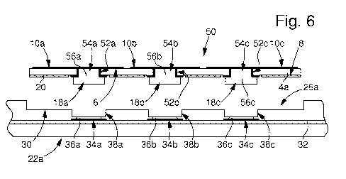
The externat connector 50 has a plurality of externat contact pads
10a to 10f. It comprises an insulating support 4a, which has a plurality of
apertures 52a, 52h, 52c (and a fourth that is flot visible in the sectional
view
of Figure 6) between its outside face 6 and its inside face 8. The apertures
of this plurality of apertures are respectively closed by the externat pads
10a, 10b, 10c and 10d forming a subassembly of the plurality of externat
metal contact pads on the side of the outside face of the insulating support
In general, these apertures are at least partially filled with the respective
metal parts 54a, 54b, 54c, which, with said respective projections 18a, 18b,
18c that surmount them or edend them and before the assembly on the
card body of the externat connector, form metal studs 56a, 56b, 56c, which
rise from the rear surfaces of said subassembly of externat pads traversing
the insulating support 4a (Figure 6). After placement of the externat
connector in its cavity 26a of the card body 22a, during which the
projections 18a, 18b, 18c penetrate into the respective individual cavities
38a, 38b, 38c, and after the supply of energy that is supplied to these metal
studs and to the truncated metal mounds 36a, 36b, 36c, metal connecting
bridges 62a, 62b, 62c are formed between the rear surfaces of said externat
pads and the corresponding internat pads to produce solder joints on the
internat pads 34a, 34b, 34c, wherein these metal connecting bridges each
comprise a solder joint on the side of the rear surface of the corresponding
externat pad that assures a soldered contact to the latter. Thus, an
CA 02873503 2014-11-13
- 15 -
electronic card 60 according to the invention such as that shown in partial
section in Figure 7 is obtained. These metal connecting bridges completely
define the electrical junctions between the internai pads in question and the
corresponding demal pads.
It will be observed, in a variant shown in the figures, that the
apertures 52a, 52b, 52c have a metal layer forming an adhesive interface
on their side wall and this layer can also extend along the periphery of the
apertures on the inside face of the insulating support to form metal rings.
During the supply of energy to conduct the soldering in particular, the solder
material bonds to this metal layer, as shown in Figure 7. In the variant
shown in this figure the apertures in the insulating support 4a are
substantially filled by the respective metal connecting bridges.
In a preferred variant the metal studs and the metal connecting
bridges obtained subsequently by the production process according to the
invention are each formed by a solder material so that the solder joint on the
side of the corresponding intemal pad and the solder joint on the side of the
rear surface of the corresponding external pad are both formed by the same
single solder joint that extends between this corresponding internai pad and
this rear surface of the corresponding external pad.
According to a particular variant the apertures have a cross-section
(in the general plane of the insulating support) that has at least one
dimension larger than 0.2 mm (200 pm). ln particular, the cross-section is
circular. According to a preferred variant the diameter of the apertures is
larger than 0.5 mm (500 pm).
According to a particular variant of the production process of the
invention the solder material forming the metal projections is deposited on
the side of the inside face of the insulating support by a nozzle that
receives
the solder material from a metering device that allows the quantity of solder
material applied to each individual cavity at the base of the cavity of the
card
body to be controlled precisely. This variant is particularly well suited to
the
CA 02873503 2014-11-13
- 16 -
formation of the metal studs in the production of the second embodiment of
an electronic card according to the invention, but it can also be used for the
production of the first embodiment described above. The deposited solder
material can, for example, be in paste form, in the form of molten metal that
hardens following the deposition or by the provision of preformed elements.
A step of shaping the projections can be provided in order to obtain a given
shape and substantially identical dimensions for ail the projections. It will
be
noted that the variants described above for the formation of the metal
projections in the framework of the first embodiment can also be used to
form the metal studs of the second embodiment. In the case where a
screen-printing technique is used, care will be taken that the metal studs
have a smaller diameter than that of the apertures 52a, 52h, 52c so that
they do flot have a projecting colla!' on their free end.
An externat connector 50a, which is a variant of the connector 50 of
Figure 6, is shown in partial section in Figure 8. This connector differs in
that
the metal studs 56a, 56b are formed by metal parts 54a, 54b formed from
solder material that has already melted once and hardened to form a solid
metal without air and/or liquid (solvent). Arranged on these metal parts are
the metal projections 18a, 18b that are formed by a solder material in paste
form that has, however, been dried after its deposition on the side of the
inside face 8 of the insulating support 4a. These projections are deposited
by a nozzle and are substantially rounded in shape. Since the individual
cavities of the card body are cylindrical, it is provided that the projections
initially, before the assembly, have a height greater than the depth of the
individual cavities. During the insertion of the projections into the
respective
cavities the projections are crushed and deformed in order to at least
partially fill the respective cavities. After the supply of energy and
soldering
of the electrical junctions an electronic card 60 such as that shown in Figure
7 is obtained. it will be noted that the solder materials of the metal parts
and
the projections can be different or of the same metal material/alloy.
CA 02873503 2014-11-13
- 17 -
Figure 9 shows the production of a plurality of externat connectors in
a strip. The insulating supports of the plurality of connectors are initially
formed by a strip 70, which comprises metal contact pads (flot shown) on
one face 71 and on the other side has intermediate contact pads, each
electrically connected to one of the externat metal contact pads, and also
apertures, which traverse the insulating support as far as the respective rear
surfaces of at least one subassembly of said metal contact pads. The strip
is firstly wound onto a first cou l 72. It is then unwound progressively and
after
having passed a first roll 74, it runs under a solder material distributor 76
comprising a nozzle or a needle 78, by means of which drops of solder
material are deposited onto each of said interrnediate contact pads or into
each of said apertures. This operation is conducted with precision, the
distributor being provided to be mobile in at least one transverse direction
to
the running direction of the strip 70 in a plane parallel to the latter. This
distributor is arranged to deposit precise metered quantities of solder
material. According to the invention the solder material defines a plurality
of
metal projections 80A. In the present case according to a variant of the
invention the solder material is deposited in paste form.
The strip 70 with the projections 80A formed from a solder material
paste then passes into an oven 82, which serves to dry and harden the
solder material. Thus, projections 80B formed from hardened solder
material exit from the oven. The oven is, for example, a hot air or uv oven.
In a particular variant the supply of heat to the projections is performed in
a
localised manner by optical diodes. Once the strip has passed through the
oven, it is unwound onto a second cou l 86 after having passed over a
second roll 84. As a result of this, a plurality of externat connectors
according to the invention can be easily stored before they are used in the
production of a plurality of electronic cards, during which the strip 70 with
the metal projections 80B is progressively unwound from the storage colt 86
and the externat connectors are then cut off from the strip to form individual
CA 02873503 2014-11-13
- 18 -
connectors that are then respectively placed into the cavities of the
plurality
of cards.
It will be noted that instead of forming the projections using the solder
material distributor, a variant provides that the projections are formed by
preformed elements, which are applied and positioned on the plurality of
connectors on a strip by an automatic installation.