Language selection

Search

Patent 2873911 Summary

Third-party information liability

Some of the information on this Web page has been provided by external sources. The Government of Canada is not responsible for the accuracy, reliability or currency of the information supplied by external sources. Users wishing to rely upon this information should consult directly with the source of the information. Content provided by external sources is not subject to official languages, privacy and accessibility requirements.

Claims and Abstract availability

Any discrepancies in the text and image of the Claims and Abstract are due to differing posting times. Text of the Claims and Abstract are posted:

  • At the time the application is open to public inspection;
  • At the time of issue of the patent (grant).
(12) Patent: (11) CA 2873911
(54) English Title: AMPLIFIER CIRCUIT WITH CROSS WIRING OF DIRECT-CURRENT SIGNALS AND MICROWAVE SIGNALS
(54) French Title: CIRCUIT AMPLIFICATEUR AVEC CABLAGE CROISE DE SIGNAUX DE COURANT CONTINU ET DE SIGNAUX HYPERFREQUENCES
Status: Granted and Issued
Bibliographic Data
(51) International Patent Classification (IPC):
  • H03F 3/20 (2006.01)
(72) Inventors :
  • ZHANG, BIN (China)
  • TAO, HONGQI (China)
(73) Owners :
  • CHINA ELECTRONICS TECHNOLOGY GROUP CORPORATION NO.55 RESEARCH INSTITUTE
(71) Applicants :
  • CHINA ELECTRONICS TECHNOLOGY GROUP CORPORATION NO.55 RESEARCH INSTITUTE (China)
(74) Agent: NORTON ROSE FULBRIGHT CANADA LLP/S.E.N.C.R.L., S.R.L.
(74) Associate agent:
(45) Issued: 2018-01-02
(86) PCT Filing Date: 2012-06-19
(87) Open to Public Inspection: 2013-11-28
Examination requested: 2015-01-16
Availability of licence: N/A
Dedicated to the Public: N/A
(25) Language of filing: English

Patent Cooperation Treaty (PCT): Yes
(86) PCT Filing Number: PCT/CN2012/077135
(87) International Publication Number: WO 2013174052
(85) National Entry: 2014-11-18

(30) Application Priority Data:
Application No. Country/Territory Date
201210161501.9 (China) 2012-05-23

Abstracts

English Abstract


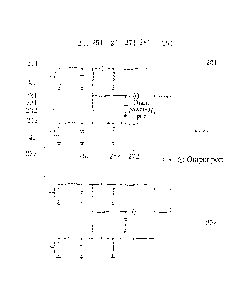
Provided is an amplifier circuit with cross wiring of direct-current signals
and
microwave signals, which includes: two branch sub-circuits (201, 202) being
mirrors
with each other and a third capacitor (2101) connected in parallel to an
output end.
The sub-circuit includes a direct-current feeding circuit and a microwave
signal
circuit. A transistor core drain power-up port (Vds) of a heterojunction field
effect
transistor (FET) of the direct-current feeding circuit is connected to a first
micro-strip
inductor (241) in series after passing through a first capacitor (281)
connected in
parallel, is respectively connected to one of a pair of third inductors (211,
212) in
series by a pair of branched second inductors (231, 232), and is respectively
connected to a transistor core drain port of the heterojunction FET. A pair of
third
inductors (211, 212) of the microwave signal circuit is respectively connected
to one
of a pair of first capacitors (251, 252) in series after respectively passing
through one
of a pair of second capacitors (221, 222) connected in parallel, is
respectively
connected to one of a pair of ground inductors (261, 262) in parallel, is
respectively
connected to one of a pair of fourth inductors (271, 272) in series, and is
combined to
be connected to an output end through a serially connected fifth inductor
(291). The
circuit has low sensitivity and a symmetrical circuit structure. Without a
severely
discontinuous region of an electromagnetic field, the layout density and the
chip space
utilization rate can be improved.


French Abstract

L'invention concerne un circuit amplificateur avec câblage croisé de signaux de courant continu et de signaux hyperfréquences, comprenant deux sous-circuits de branche (201, 202) qui sont des miroirs l'un de l'autre et un troisième condensateur (2101) connecté en parallèle à une extrémité de sortie. Chaque sous-circuit comprend un circuit d'alimentation en courant continu et un circuit de signal hyperfréquences. Un port de mise sous tension du drain d'un noyau d'un tube à effet de champ à hétérojonction (Vds) du circuit d'alimentation en courant continu est connecté à un premier inducteur à micro-ruban (241) en série après passage à travers un premier condensateur parallèle monté en parallèle, est connecté respectivement à un inducteur d'une paire de troisièmes inducteurs (211, 212) par une paire de seconds inducteurs banchés (231, 232) et est connecté respectivement à une extrémité de drain d'un noyau d'un tube à effet de champ à hétérojonction. Une paire de troisièmes inducteurs (211, 212) du circuit de signal hyperfréquences est connectée respectivement à un condensateur d'une paire de premiers condensateurs (251, 252) en série après passage à travers un condensateur d'une paire de deuxièmes condensateurs (221, 222) connectés en parallèle, est connectée à un inducteur d'une paire d'inducteurs de masse (261, 262) en parallèle, est connectée respectivement à un inducteur d'une paire de quatrièmes inducteurs (271, 272) en série et est connectée à une extrémité de sortie par un cinquième inducteur (291) connecté en série. Le circuit présente les avantages d'une faible sensibilité et d'une structure de circuit symétrique. Comme le circuit ne présente pas de grave zone de discontinuité d'un champ électromagnétique, il est possible d'améliorer la densité de territoire et le rapport d'utilisation de l'espace de la puce.

Claims

Note: Claims are shown in the official language in which they were submitted.


CLAIMS
What is claimed is:
1. A amplifier circuit with cross wiring of direct-current signals and
microwave
signals, comprising two branch sub-circuits (201, 202) being mirrors with each
other
and a third capacitor (2101) connected in parallel to an output end, wherein
the
sub-circuit comprises a direct-current feeding circuit and a microwave signal
circuit,
the direct-current feeding circuit is mainly formed of a transistor core drain
power-up
port (Vds) of a heterojunction field effect transistor (FET), a first
capacitor (281), a
first micro-strip inductor (241), a pair of second inductors (231, 232), and a
pair of
third inductors (211, 212), the transistor core drain power-up port (Vds) of
the
heterojunction FET is connected to the first micro-strip inductor (241) in
series after
passing through the first capacitor (281) connected in parallel, is
respectively
connected to one of a pair of third inductors (211, 212) in series by a pair
of branched
second inductors (231, 232), and is respectively connected to a transistor
core drain
port of the heterojunction FET, the microwave signal circuit is mainly formed
of a
pair of third inductors (211, 212), a pair of second capacitors (221, 222), a
pair of first
capacitors (251, 252), a pair of ground inductors (261, 262), a pair of fourth
inductors
(271, 272), and a fifth inductor (291), and the pair of third inductors (211,
212) is
respectively connected to one of the pair of first capacitors (251, 252) in
series after
respectively passing through one of the pair of second capacitors (221, 222)
connected in parallel, is respectively connected to one of the pair of ground
inductors
(261, 262) in parallel, is respectively connected to one of the pair of fourth
inductors
(271, 272) in series, and is combined to be connected to an output end through
the
serially connected fifth inductor (291).
2. The amplifier circuit with cross wiring of direct-current signals and
microwave
signals according to claim 1, wherein a three-dimensional cross is formed
between
any serially connected inductor of the direct-current feeding circuit and any
serially
connected inductor of the microwave signal circuit.
3. The amplifier circuit with cross wiring of direct-current signals and
microwave
signals according to claim 2, wherein an air bridge structure is adopted for
the
three-dimensional cross .
4. The amplifier circuit with cross wiring of direct-current signals and
microwave
signals according to claim 3, wherein lumped inductors are adopted for the
first
8

CLAIMS
inductor and the pair of second inductors in the direct-current feeding
circuit and the
pair of fourth inductors and the fifth inductor in the microwave signal
circuit.
5. The amplifier circuit with cross wiring of direct-current signals and
microwave
signals according to claim 3, wherein distributed micro-strip lines are
adopted for the
first inductor and the pair of second inductors in the direct-current feeding
circuit and
the pair of fourth inductors and the fifth inductor in the microwave signal
circuit.
6. The amplifier circuit with cross wiring of direct-current signals and
microwave
signals according to claim 4 or 5, wherein outputs of the two subunits (201,
202) that
are mirror circuits with each other are combined to reach an output (Pout)
port
through the parallel connected third capacitor (2101).
7. The amplifier circuit with cross wiring of direct-current signals and
microwave
signals according to claim 6, wherein the heterojunction FET is a
high-electron-mobility transistor (HEMT).
8. The amplifier circuit with cross wiring of direct-current signals and
microwave
signals according to claim 7, wherein a transistor core of the HEMT is
extended into 8
cells, and every two cells are combined to be respectively connected to one of
the
serially connected third inductors (211, 212).
9

Description

Note: Descriptions are shown in the official language in which they were submitted.


CA 2873911 2017-05-29
DESCRIPTION
AMPLIFIER CIRCUIT WITH CROSS WIRING OF
DIRECT-CURRENT SIGNALS AND MICROWAVE SIGNALS
FIELD OF THE INVENTION
100011 The present invention relates to an amplifier circuit with cross wiring
of direct-current
signals and microwave signals, and more particularly to a microwave and
millimeter-wave
high-power monolithic integrated power amplifier circuit with cross wiring of
direct-current
signals and microwave signals, and belongs to the field of communications
technologies.
DESCRIPTION OF RELATED ART
[0002] A microwave and millimeter-wave high-power monolithic integrated power
amplifier
is a core device in a microwave detection and guidance system and is used for
amplifying a
low-power signal into a high-power signal, so as to increase power and a
radiation level of an
emitter in the system, thereby increasing a detection distance. With the
development of a
microwave detection and guidance system, it is required to increase a
detection distance and
also reduce energy consumption, thereby improving efficiency of the amplifier.
[0003] In an aspect, a microwave and millimeter-wave high-power monolithic
integrated
power amplifier is required to have high output power and high efficiency. In
another
aspect, during batch production, to improve consistency and the yield rate and
reduce the cost,
a chip must be miniaturized.
[0004] High-power output requires supply of a large current, and therefore, to
bear a large
current, a feeding circuit usually has a line width of 100 kan, which is more
than twice as
large as the width of a signal line, occupies 1/10 of a radial distance of a
chip tail-level space,
and occupies a large chip area. In addition, the acquisition of high power and
high
efficiency requires proper matching at an output end. Common T and 71-
matching circuits
and several branches of derivative forms thereof are easy to make flexible
adjustment in the
circuit design and layout for signals in different frequency bands,
especially, broadband
signals. Due to the limit of the chip size, a microwave and millimeter-wave
high-power
monolithic integrated power amplifier chip has a very limited wiring space in
a tail-level
circuit layout.

CA 2873911 2017-05-29
DESCRIPTION
[0005] A tail-level unit in an existing microwave and millimeter-wave high-
power monolithic
integrated power amplifier has a large grid-width transistor core and low
output impedance.
A typical structure is shown in FIG. 1. A tail-level transistor core 170
passes through two
mirrored output circuits 101, 102, and reaches an output port 112 after being
connected to an
inductor 134 in series and connected to a capacitor 135 in parallel. An output
subcircuit 101
includes a Vds port 111, a capacitor 121 connected in parallel, a capacitor
131 connected in
series, a ground micro-strip 132 connected in parallel, micro-strip lines 122,
133, a
micro-strip combining unit 151, capacitors 141, 142 in parallel, and micro-
strip combining
units 161, 162. The disadvantage of the circuit implemented in this manner is
that passing
through the parallel connected capacitors 141, 142, the matching unit needs
combining first
to be connected to the capacitor 131, which limits the freedom of the circuit
design.
Meanwhile, the serially connected capacitor 131 and the parallel connected
ground
micro-strip 132 have very high sensitivity to performance. Also, the
electromagnetic field
of a region 1 is discontinuous, and the microwave matching circuit is also not
completely
symmetrical about the transistor core. For a matching circuit having a large
grid width, high
power, and a high impedance transformation ratio, the performance of the
matching circuit
will be significantly limited.
SUMMARY OF THE INVENTION
Technical Problem
[0006] The task of the present invention is to propose an amplifier circuit
with cross wiring of
direct-current signals and microwave signals, so as to fully explore the
performance of a large
grid width transistor core, and significantly improve layout density and a
chip space
utilization rate, thereby solving the problem of matching of a broadband
circuit having a high
impedance ratio of a large grid width power chip.
Technical Solution
[0007] A transistor core direct-current feeding circuit and a microwave signal
circuit are
completely symmetrical about a high-electron-mobility transistor (HEMT) cell,
so as to fully
exert the performance of a transistor core FET. Meanwhile, a parallel
connected second
capacitor may be directly connected to a capacitor in series, thereby
improving the freedom
of circuit design. Compared with the prior art, a serially connected capacitor
(131) is
implemented by serially connected first capacitors (251, 252), and a parallel
connected
2

CA 2873911 2017-05-29
DESCRIPTION
ground micro-strip (132) is implemented by parallel connected ground inductors
(261, 262);
therefore, the circuit sensitivity of elements in the present invention is
lowered. Meanwhile,
the solution of the present invention has a symmetrical circuit structure, and
a severely
discontinuous region of an electromagnetic field does not exist.
[0008] To achieve the foregoing task, the basic technical solution of an
amplifier circuit with
cross wiring of direct-current signals and microwave signals of the present
invention is
formed of two branch sub-circuits (201, 202) being mirrors with each other and
a third
capacitor (2101) connected in parallel to an output end. The sub-circuit
includes a
direct-current feeding circuit and a microwave signal circuit. The direct-
current feeding
circuit is mainly formed of a transistor core drain power-up port (Vds) of a
heterojunction
field effect transistor (FET), a first capacitor (281), a first micro-strip
inductor (241), a pair of
second inductors (231, 232), and a pair of third inductors (211, 212). The
transistor core
drain power-up port (Vds) of the heterojunction FET is connected to a first
micro-strip
inductor (241) in series after passing through the first capacitor (281)
connected in parallel, is
respectively connected to one of the pair of third inductors (211, 212) in
series by the pair of
branched second inductors (231, 232), and is respectively connected to a drain
port of the
heterojunction FET core. The microwave signal circuit is mainly formed of a
pair of third
inductors (211, 212), a pair of second capacitors (221, 222), a pair of first
capacitors (251,
252), a pair of ground inductors (261, 262), a pair of fourth inductors (271,
272), and a fifth
inductor (291). The pair of third inductors (211, 212) is respectively
connected to one of the
pair of first capacitors (251, 252) in series after respectively passing
through one of the pair
of second capacitors (221, 222) connected in parallel, is respectively
connected to one of the
pair of ground inductors (261, 262) in parallel, is respectively connected to
one of the pair of
fourth inductors (271, 272) in series, and is combined to be connected to an
output end
through the serially connected fifth inductor (291).
[0009] A further improvement in the technical solution of the present
invention is that a
three-dimensional cross is formed between any serially connected inductor of
the
direct-current feeding circuit and any serially connected inductor of the
microwave signal
circuit, and a three-dimensional cross between a microwave signal and a direct-
current signal
is implemented in an air bridge manner.
[0010] Yet a further improvement in the technical solution of the present
invention is that
lumped inductors or distributed micro-strip lines are adopted for the first
inductor and the pair
3

CA 2873911 2017-05-29
DESCRIPTION
of second inductors in the direct-current feeding circuit and the pair of
fourth inductors and
the fifth inductor in the microwave signal circuit.
[0011] Another further improvement in the technical solution of the present
invention is that
outputs of two subunits that are mirror circuits with each other are combined
to reach an
output (Pout) port through the parallel connected third capacitor.
[0012] Yet another further improvement in the technical solution of the
present invention is
that the heterojunction FET is a HEMT, the transistor core of the HEMT may be
extended
into 8 cells, and every two cells are combined to be connected to one of the
serially connected
third inductors (211, 212).
Advantageous Effect
[0013] After the foregoing technical solution of the present invention is
adopted, a transistor
core direct-current feeding circuit and a microwave signal circuit are
completely symmetrical
about a HEMT cell, so as to fully exert the performance of a transistor core
FET.
Meanwhile, a parallel connected second capacitor may be directly connected to
a capacitor in
series, thereby improving the freedom of circuit design. Compared with the
prior art, a
serially connected capacitor (131) is implemented by serially connected first
capacitors (251,
252), and a parallel connected ground micro-strip (132) is implemented by
parallel connected
ground inductors (261, 262); therefore, the circuit sensitivity of elements in
the present
invention is lowered. Meanwhile, the solution of the present invention has a
symmetrical
circuit structure, a severely discontinuous region of an electromagnetic field
does not exist,
and thc layout density and the chip space utilization rate can be
significantly improved.
BRIEF DESCRIPTION OF THE DRAWINGS
[0014] The present invention is further described below with reference to the
accompanying
drawings.
[0015] FIG. 1 shows a tail-level circuit layout of a microwave and millimeter-
wave
high-power monolithic integrated power amplifier in the prior art;
[0016] FIG. 2 is a principle view of an amplifier circuit with cross wiring of
direct-current
signals and microwave signals according to the present invention; and
[0017] FIG. 3 shows a tail-level circuit layout of a microwave and millimeter-
wave
4

CA 2873911 2017-05-29
DESCRIPTION
high-power monolithic integrated power amplifier according to an embodiment of
the present
invention. The numerals 301, 302, and so on in FIG. 3 correspond to 201, 202,
and so on in
FIG. 2 respectively, and the like.
DETAILED DESCRIPTION OF THE INVENTION
[0018] Embodiment 1
[0019] An amplifier circuit with cross wiring of direct-current signals and
microwave signals
in this embodiment is fabricated by using a semiconductor monolithic microwave
integrated
circuit (MMIC) process line, the principle view of the circuit is shown in
FIG. 2, and the
circuit layout is shown in FIG. 3. During the implementation of the circuit, a
serially
connected inductor is implemented by using micro-strip lines having different
impedance,
and a capacitor is implemented by using a lumped Metal-Insulator-Metal (MIM)
capacitor.
The circuit is formed of two circuit network units 301, 302 that are
consistent in amplitude
and phase of microwave power signals and are mirror circuits with each other.
Each circuit
network unit is formed of a direct-current feeding circuit and a microwave
signal circuit.
The direct-current signal circuit includes a transistor core drain power-up
port VdS of a
HEMT, a first MIM capacitor 381 connected in parallel, a first micro-strip
line 341 connected
in series, second micro-strip lines 331, 332 connected in series, and third
micro-strip lines
311, 312 connected in series. The microwave signal circuit includes third
micro-strip lines
311, 312 connected in series, sccond MIM capacitors 321, 322 connected in
parallel, first
MIM capacitors 351, 352 connected in series, ground micro-strip lines 361, 362
connected in
parallel, fourth micro-strip lines 371, 372 connected in series, and a fifth
micro-strip line 391
connected in series. The circuit network units 301, 302 are combined to reach
an output
port Pout through a parallel connected third MIM capacitor 3101. A three-
dimensional
cross is implemented between the second micro-strip 332 connected in series in
the
direct-current feeding circuit of the circuit and the fifth micro-strip 391
connected in series in
the microwave signal circuit. The implementation manner of the cross uses an
air bridge
3111 for bridging. The outputs of the two subunits that are mirror circuits
with each other
are combined to reach the output (Pout) port through the parallel connected
third capacitor.
The transistor core of the HEMT is extended into 8 cells, and every two cells
are combined to
be connected to one of the third inductors 211, 212 connected in series.
[0020] In the circuit units 301, 302, a direct-current feeding signal is
transmitted in a

CA 2873911 2017-05-29
DESCRIPTION
transverse direction on a chip, and a microwave power signal is transmitted in
an axial
direction; such a circuit wiring manner may reduce crosstalk influence on a
microwave power
signal from noise that has various frequency components and is from a direct-
current power
source. For a circuit chip, a working frequency band, power, efficiency,
consistency, a yield
rate, and cost are taken into comprehensive consideration; the wafer in the
chip uses a GaAs
or GaN material as a substrate; however, the present invention is not only
limited thereto.
[0021] Persons skilled in the art can easily conceive a three-dimensional
cross between any
serially connected inductor of the direct-current feeding circuit and any
serially connected
inductor of the microwave signal circuit according to the foregoing
embodiment.
Distributed micro-strip lines or lumped inductors may be adopted for the first
inductor and
the pair of second inductors in the direct-current feeding circuit and the
pair of fourth
inductors and the fifth inductor in the microwave signal circuit. In addition,
in addition to a
HEMT, the heterojunction FET may also be a modulation-doped FET (MODFET), a
two-dimensional electron gas FET (2-DEGFET), a selectively doped
heterojunction transistor
(SDHT), and the like.
[0022] It is proved through theory and tests that, this embodiment has the
following
advantageous effects:
[0023] 1) A direct-current feeding circuit and a microwave signal circuit are
completely
symmetrical about a transistor core, and therefore, for every cell, the
impedance of a load
circuit of the cell is completely same, making it easy to exert the optimal
performance of a
transistor core.
[0024] 2) A parallel connected second MIM capacitor is directly connected to a
second
capacitor connected in series. The freedom of the chip design is no longer
limited by a fixed
position of an intersecting point between a direct-current signal and a
microwave power
signal.
[0025] 3) The circuit structure is relatively symmetrical, and the
electromagnetic field is
relatively continuous and homogeneous.
[0026] 4) In the microwave signal circuit, the serially connected first MIM
capacitor and a
parallel connected ground micro-strip significantly lower the sensitivity to
the circuit
performance. Therefore, sufficient discrete allowance is left for process
processing, and
6

CA 2873911 2017-05-29
DESCRIPTION
mass production of chips becomes casy.
[0027] 5) For circuit design with more cells, an eight-cell structure may be
conveniently
extended, thereby facilitating chip design of higher power.
[0028] 6) A chip space utilization rate is improved, and chip cost is lowered.
[0029] In sum, this embodiment solves the difficult problem of matching from
the output
impedance of the large grid width power chip to a broadband having a high
impedance ratio
and a 50-ohm port, so as to fully explore high power and high efficiency
performance of a
large grid width transistor core.
7

Representative Drawing
A single figure which represents the drawing illustrating the invention.
Administrative Status

2024-08-01:As part of the Next Generation Patents (NGP) transition, the Canadian Patents Database (CPD) now contains a more detailed Event History, which replicates the Event Log of our new back-office solution.

Please note that "Inactive:" events refers to events no longer in use in our new back-office solution.

For a clearer understanding of the status of the application/patent presented on this page, the site Disclaimer , as well as the definitions for Patent , Event History , Maintenance Fee  and Payment History  should be consulted.

Event History

Description Date
Common Representative Appointed 2019-10-30
Inactive: Late MF processed 2019-10-24
Letter Sent 2019-06-19
Grant by Issuance 2018-01-02
Inactive: Cover page published 2018-01-01
Inactive: Final fee received 2017-11-21
Pre-grant 2017-11-21
Letter Sent 2017-10-20
Notice of Allowance is Issued 2017-10-20
Inactive: QS passed 2017-10-17
Inactive: Approved for allowance (AFA) 2017-10-17
Reinstatement Requirements Deemed Compliant for All Abandonment Reasons 2017-06-20
Letter Sent 2017-06-20
Deemed Abandoned - Failure to Respond to Maintenance Fee Notice 2017-06-19
Amendment Received - Voluntary Amendment 2017-05-29
Inactive: S.30(2) Rules - Examiner requisition 2017-01-04
Inactive: Report - No QC 2017-01-04
Inactive: Q2 failed 2016-12-22
Amendment Received - Voluntary Amendment 2016-07-18
Inactive: S.30(2) Rules - Examiner requisition 2016-01-19
Inactive: Report - No QC 2016-01-19
Letter Sent 2015-01-30
Inactive: Cover page published 2015-01-20
All Requirements for Examination Determined Compliant 2015-01-16
Request for Examination Requirements Determined Compliant 2015-01-16
Request for Examination Received 2015-01-16
Inactive: First IPC assigned 2014-12-11
Inactive: Notice - National entry - No RFE 2014-12-11
Inactive: IPC assigned 2014-12-11
Application Received - PCT 2014-12-11
National Entry Requirements Determined Compliant 2014-11-18
Application Published (Open to Public Inspection) 2013-11-28

Abandonment History

Abandonment Date Reason Reinstatement Date
2017-06-19

Maintenance Fee

The last payment was received on 2017-06-20

Note : If the full payment has not been received on or before the date indicated, a further fee may be required which may be one of the following

  • the reinstatement fee;
  • the late payment fee; or
  • additional fee to reverse deemed expiry.

Patent fees are adjusted on the 1st of January every year. The amounts above are the current amounts if received by December 31 of the current year.
Please refer to the CIPO Patent Fees web page to see all current fee amounts.

Owners on Record

Note: Records showing the ownership history in alphabetical order.

Current Owners on Record
CHINA ELECTRONICS TECHNOLOGY GROUP CORPORATION NO.55 RESEARCH INSTITUTE
Past Owners on Record
BIN ZHANG
HONGQI TAO
Past Owners that do not appear in the "Owners on Record" listing will appear in other documentation within the application.
Documents

To view selected files, please enter reCAPTCHA code :


To view images, click a link in the Document Description column. To download the documents, select one or more checkboxes in the first column and then click the "Download Selected in PDF format (Zip Archive)" or the "Download Selected as Single PDF" button.

List of published and non-published patent-specific documents on the CPD .

If you have any difficulty accessing content, you can call the Client Service Centre at 1-866-997-1936 or send them an e-mail at CIPO Client Service Centre.


Document
Description 
Date
(yyyy-mm-dd) 
Number of pages   Size of Image (KB) 
Claims 2017-05-28 2 76
Description 2017-05-28 7 308
Description 2014-11-17 7 330
Claims 2014-11-17 2 81
Drawings 2014-11-17 3 39
Abstract 2014-11-17 1 34
Representative drawing 2014-11-17 1 9
Abstract 2017-11-26 1 32
Representative drawing 2017-12-13 1 6
Maintenance fee payment 2024-05-20 56 2,325
Notice of National Entry 2014-12-10 1 193
Acknowledgement of Request for Examination 2015-01-29 1 188
Courtesy - Abandonment Letter (Maintenance Fee) 2017-06-19 1 172
Notice of Reinstatement 2017-06-19 1 163
Commissioner's Notice - Application Found Allowable 2017-10-19 1 163
Maintenance Fee Notice 2019-07-30 1 180
Late Payment Acknowledgement 2019-10-28 1 163
Late Payment Acknowledgement 2019-10-28 1 162
PCT 2014-11-17 4 172
Examiner Requisition 2016-01-18 3 226
Amendment / response to report 2016-07-17 2 107
Examiner Requisition 2017-01-03 3 167
Amendment / response to report 2017-05-28 11 479
Maintenance fee payment 2017-06-19 1 28
Final fee 2017-11-20 1 67