Note: Descriptions are shown in the official language in which they were submitted.
CA 02874560 2014-11-21
WO 2013/184638
PCT/US2013/044028
STRAIN CONTROL FOR ACCELERATION OF EPITAXIAL LIFT-OFF
Cross-Reference to Related Application
[001] This application claims the benefit of priority to U.S. Provisional
Patent
Application No. 61/655,084, filed on June 4, 2012, which is incorporated by
reference
herein in its entirety.
Statement Regarding Federally Sponsored Research
[002] This invention was made with Government support under W911nF-08-2-
0004 awarded by the Army Research Office. The government has certain rights in
the
invention.
Joint Research Agreement
[003] The subject matter of this application was made by, on behalf of, and/or
in
connection with one or more of the following parties to a joint university-
corporation
research agreement: University of Michigan and Global Photonic Energy
Corporation.
The agreement was in effect on and before the date the subject matter of this
application
was made, and such was made as a result of activities undertaken within the
scope of the
agreement.
[004] The disclosure generally relates to methods of making, electrically
active,
optically active, solar, semiconductor and thin-film materials, such as
photovoltaic (PV)
devices through the use of epitaxial lift off (ELO).
[005] Photosensitive optoelectronic devices convert electromagnetic radiation
into electricity. Solar cells, also called PV devices, are a type of
photosensitive
optoelectronic device that is specifically used to generate electrical power.
PV devices,
which may generate electrical energy from light sources other than sunlight,
can be used
to drive power consuming loads to provide, for example, lighting, heating, or
to power
1
CA 02874560 2014-11-21
WO 2013/184638
PCT/US2013/044028
electronic circuitry or devices such as calculators, radios, computers or
remote monitoring
or communications equipment.
[006] To produce internally generated electric fields, the usual method is to
juxtapose two layers of material with appropriately selected conductive
properties,
especially with respect to their distribution of molecular quantum energy
states. The
interface of these two materials is called a photovoltaic junction. In
traditional
semiconductor theory, materials for forming PV junctions have been denoted as
generally
being of either n or p type. Here n-type denotes that the majority carrier
type is the
electron. This could be viewed as the material having many electrons in
relatively free
energy states. The p-type denotes that the majority carrier type is the hole.
Such material
has many holes in relatively free energy states. The type of the background,
i.e., not
photo-generated, majority carrier concentration depends primarily on
unintentional
doping by defects or impurities. The type and concentration of impurities
determine the
value of the Fermi energy, or level, within the gap between the conduction
band
minimum and valance band maximum energies. The Fermi energy characterizes the
statistical occupation of molecular quantum energy states denoted by the value
of energy
for which the probability of occupation is equal to 1/2. A Fermi energy near
the
conduction band minimum energy indicates that electrons are the predominant
carrier. A
Fermi energy near the valence band maximum energy indicates that holes are the
predominant carrier. Accordingly, the Fermi energy is a primary characterizing
property
of traditional semiconductors and the prototypical PV junction has
traditionally been the
p-n interface.
[007] Conventional inorganic semiconductor PV cells employ a p-n junction to
establish an internal field. High-efficiency PV devices are typically produced
on
expensive, single crystal growth substrates. These growth substrates may
include single
2
CA 02874560 2014-11-21
WO 2013/184638
PCT/US2013/044028
crystal wafers, which can be used for creating a perfect lattice and
structural support for
the epitaxial growth of active layers, also known as "epilayers." These
epilayers may be
integrated into PV devices with their original growth substrates intact.
Alternatively,
those epilayers may be removed and recombined with a host substrate.
[008] In some instances, it may be desirable to transfer the epilayers to host
substrates that exhibit desirable optical, mechanical, or thermal properties.
For example,
Gallium Arsenide (GaAs) epilayers may be grown on Silicon (Si) substrates.
However,
the electronic quality of the resulting material may be insufficient for
certain electronic
applications. Therefore, it may be desirable to preserve the high material
quality of the
lattice-matched epilayers, while allowing the integration of those epilayers
into other
substrates. This may be accomplished by a method known as epitaxial liftoff In
epitaxial
liftoff processes, epilayers may be "lifted off' growth layers and recombined
(e.g.,
bonded or adhered) to a new host substrate.
[009] Although they may provide desirable epitaxial growth characteristics,
typical growth substrates can be thick and create excess weight, and the
resulting devices
tend to be fragile and require bulky support systems. Epitaxial liftoff may be
a desirable
way to transfer epilayers from their growth substrates to more efficient,
light-weight, and
flexible host substrates. Given the relative scarcity of typical growth
substrates and the
desirable characteristics that they impart on resulting cell structures, it
may be desirable to
recycle and/or reuse growth substrates in subsequent epitaxial growths.
[010] The ELO process is attractive for solar cell applications and provides
for a
potential reduction of production cost for III-V based device by reusing the
parent wafers.
For the optoelectronic devices, such as photovoltaic cells and photodetectors,
it requires
approximately half of the active-region thickness to absorb an equivalent
amount of
incident radiation compared to conventional substrate wafer-based devices by
fabricating
3
CA 02874560 2014-11-21
WO 2013/184638
PCT/US2013/044028
the thin film devices with back side reflector. Thinner active layer also
enables
production cost reduction by reducing materials consumption and growth time
for the
epitaxial layers. Furthermore, the back-side reflector prevents parasitic
absorption of
photons emitted via luminescence into the substrate and allows for increased
"photon
recycling," a necessary requirement for achieving the Shockley-Queisser Limit.
This
photon recycling allows for increased open circuit voltage in lifted off cells
as compared
to substrate cells.
[011] To accelerate the lateral etching process of the sacrificial layer, a
curvature
to a lifted off thin film and flexible handle material (e.g. plastic, wax,
metal foil,
photoresist, etc) is generally applied. This is done by bending away from the
wafer using
weight or curving the handle to open a gap between the wafer and the epi-
layer. However,
this process requires a precise epi-layer support set-up or an additional
transfer step.
Further, if the epi-layer support setup induces too much strain on the
epilayer or too much
film curvature, cracks in the thin single crystal film can result.
[012] There remains a need to expedite the ELO process by controlling the
strain
on the handle and simplifying the lift-off set-up.
[013] One embodiment of the present disclosure is directed to a thin film
device
for epitaxial lift off comprising a handle and one or more straining layers
disposed on the
handle, wherein the one or more straining layers induce a curvature of the
handle.
[014] In another embodiment, the present disclosure is directed to a thin film
device for epitaxial lift off comprising a growth substrate, a handle, and one
or more
straining layers disposed on at least one of the growth substrate and the
handle, wherein
the handle optionally having the one or more straining layers disposed thereon
is bonded
to the growth substrate, and wherein the one or more straining layers induce
at least one
strain on the handle chosen from tensile strain, compressive strain and near-
neutral strain.
4
CA 02874560 2014-11-21
WO 2013/184638
PCT/US2013/044028
[015] In another embodiment, the present disclosure is directed to a thin film
device for epitaxial lift off comprising an epilayer disposed on a growth
substrate, a
handle, and one or more straining layers disposed on at least one of the
growth substrate
and the handle, wherein the handle optionally having the one or more straining
layers
disposed thereon is bonded to the growth substrate, and wherein the one or
more straining
layers induce at least one strain on at least one of the handle and epilayer
chosen from
tensile strain, compressive strain, and near-neutral strain. In some
embodiments, the one
or more straining layers induce at least one strain on the handle and the
epilayer.
[016] In another embodiment, the present disclosure is directed to a thin film
device for epitaxial lift off comprising a sacrificial layer and an epilayer
disposed on a
growth substrate, a handle, and one or more straining layers disposed on at
least one of
the growth substrate and the handle, wherein the handle optionally having the
one or
more straining layers disposed thereon is bonded to the growth substrate, and
wherein the
one or more straining layers induce at least one strain on at least one of the
sacrificial
layer, the epilayer and the handle chosen from tensile strain, compressive
strain, and near-
neutral strain. In some embodiments, the one or more straining layers induce
at least one
strain on the sacrificial layer, the epilayer, and the handle.
[017] In another embodiment, the present disclosure provides a thin film
device
for epitaxial lift off comprising at least one sacrificial layer, and at least
one straining
layer disposed on a handle, wherein the straining layer is composed of at
least one
material chosen from a metal, a semiconductor, a dielectric and a non-metal,
and wherein
the straining layer induces a curvature of the handle.
[018] In yet another embodiment, the present disclosure provides a thin film
device for epitaxial lift off comprising at least one sacrificial layer, and
at least one
straining layer disposed on a handle, wherein the straining layer is composed
of at least
CA 02874560 2014-11-21
WO 2013/184638
PCT/US2013/044028
one material chosen from a metal, a semiconductor, a dielectric and a non-
metal, and
wherein the handle is amenable to curvature under tensile or compressive
strain from the
straining layer.
[019] In another embodiment, the present disclosure provides for a straining
layer composed of a metal. Suitable examples of this metal include pure metals
such as
Gold, Nickel, Silver, Copper, Tungsten, Platinum, Palladium, Tantalum,
Molybdenum, or
Chromium, or metal alloys containing Iridium, Gold, Silver, Copper, Tungsten,
Platinum,
Palladium, Tantalum, Molybdenum, and/or Chromium.
[020] In some embodiments of the present disclosure, the straining layer
induces
curvature of a handle. In some embodiments, the one or more straining layers
induce
curvature of the handle upon etching the sacrificial layer. In some
embodiments, the one
or more straining layers induce curvature of the handle upon parting with the
growth
substrate. In some embodiments, the curvature of the handle is toward a growth
substrate. In some embodiments, the straining layer induces a curvature of the
handle
away from a growth substrate. In some embodiments, the straining layer
minimizes
curvature of the handle.
[021] In one embodiment, the present disclosure provides for a method of
fabricating a thin film device for epitaxial lift off comprising, depositing
one or more
straining layers on a handle, wherein the one or more straining layers induce
at least one
strain on the handle chosen from tensile strain, compressive strain and near-
neutral strain.
In some embodiments, the method can induce a curvature of the handle.
[022] In another embodiment, the present disclosure provides a straining layer
which induces tensile strain to induce a curvature of the handle towards a
growth
substrate.
6
CA 02874560 2014-11-21
WO 2013/184638
PCT/US2013/044028
[023] In one embodiment, the present disclosure provides a method of
fabricating a thin film device for epitaxial lift off comprising, providing a
growth
substrate and a handle, depositing one or more straining layers on at least
one of the
growth substrate and the handle, and bonding the handle optionally having the
one or
more straining layers disposed thereon to the growth substrate.
[024] In yet another embodiment, the present disclosure provides a method for
epitaxial lift off comprising, depositing an epilayer over a sacrificial layer
disposed on a
growth substrate; depositing one or more straining layers on at least one of
the growth
substrate and a handle; bonding the handle to the growth substrate; and
etching the
sacrificial layer.
[025] A further embodiment of the present disclosure is directed to a thin
film
solar cell device comprising at least one layer disposed on a growth substrate
that is
bonded to a handle, wherein the handle is both sufficiently flexible and has a
curvature
that expedites epitaxial lift off Another embodiment of the present disclosure
is directed
to a thin film solar cell device comprising at least one layer disposed on a
growth
substrate that is bonded to a handle, wherein a difference in coefficient of
thermal
expansion between the wafer and handle is used to create a curvature in the
handle to
expedite epitaxial lift off
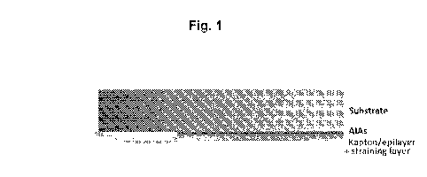
[026] Figure 1 depicts an exemplary embodiment of a thin film device for
epitaxial lift off comprising a growth substrate and a handle, e.g., a Kapton
sheet, wherein
a straining layer induces a curvature of the handle.
[027] Figure 2 depicts various combinations of sputtered Jr with tensile and
compressive strain having a single stressor layer on top of handle (a), on
bottom of handle
(b), or multiple layers on top of handle with varying strains (c), or layers
with variable
strains on both sides of the handle (d).
7
CA 02874560 2014-11-21
WO 2013/184638
PCT/US2013/044028
[028] Figure 3 depicts a 50 lam Kapton sheet with 3.5 nm, 10.5 nm, 21 nm and
42 nm thick sputtered Jr under 7 mTorr sputtering chamber pressure and with 7
nm and
28 nm sputtered Jr under 8.5 mTon- sputtering chamber pressure and a control
sheet
without Jr.
[029] Figure 4 depicts a picture of a cold-weld bonded and lifted off thin
film on
a strained handle.
[030] As used herein, the term "layer" refers to a member or component of a
photosensitive device whose primary dimension is X-Y, i.e., along its length
and width,
and is typically perpendicular to the plane of incidence of the illumination.
It should be
understood that the term "layer" is not necessarily limited to single layers
or sheets of
materials. A layer can comprise laminates or combinations of several sheets of
materials.
In addition, it should be understood that the surfaces of certain layers,
including the
interface(s) of such layers with other material(s) or layers(s), may be
imperfect, wherein
said surfaces represent an interpenetrating, entangled or convoluted network
with other
material(s) or layer(s). Similarly, it should also be understood that a layer
may be
discontinuous, such that the continuity of said layer along the X-Y dimension
may be
disturbed or otherwise interrupted by other layer(s) or material(s).
[031] As used herein, the term "III-V material" may be used to refer to
compound crystals containing elements from group IIIA and group VA of the
periodic
table. More specifically, the term III-V material may be used herein to refer
to
compounds which are combinations of the group of Gallium (Ga), Indium (In) and
Aluminum (Al), and the group of Arsenic (As), Phosphorous (P), Nitrogen (N),
and
Antimony (Sb). Representative materials may include GaAs, InP, InGaAs, AlAs,
AlGaAs, InGaAsP, InGaAsPN, GaN, InGaN, InGaP, GaSb, GaAlSb, InGaTeP, and InSb
and all related compounds. The term "Group IV" comprises such semiconductors
as Si
8
CA 02874560 2014-11-21
WO 2013/184638
PCT/US2013/044028
and Ge in column IVA of the periodic chart. Group II-VI comprises such
semiconductors
as CdS and CdTe, for example, that reside in Groups IIA and VIA of the
periodic chart.
[032] As used herein, the expression "disposed on" permits other materials or
layers to exist between a material being disposed and the material on which it
is disposed.
Likewise, the expression "bonded to" permits other materials or layers to
exist between a
material being bonded and the material to which it is bonded.
[033] As used herein, a straining layer that induces a curvature of a handle
toward a growth substrate means that the straining layer induces the handle to
take a
concave shape from the point of reference of the growth substrate.
[034] As used herein, a straining layer that induces a curvature of a handle
away
from a growth substrate means that the straining layer induces the handle to
take a convex
shape from the point of reference of the growth substrate.
[035] The term "strain" as used herein can be defined in terms of the residual
strain in the deposited layer. The strain can be tensile, compressive or near-
neutral. A
tensile strain will curve the handle towards the straining layer, a
compressive strain will
curve the handle away from the straining layer, and a near-neutral strain will
not cause
any significant curvature to the handle. In one embodiment, the strain applied
to a handle
material is tensile which accelerates curvature of the handle towards a wafer.
[036] The thin film devices described herein may be photosensitive devices. In
some embodiments, the thin film devices described herein are solar cell
devices..
[037] The present disclosure also relates to employing a protection layer
disposed between a growth substrate and at least one epitaxial layer. U.S.
Patent No.
8,378,385 and U.S. Patent Publication No. 2013/0043214 are hereby incorporated
by
reference for their disclosure of growth structures and materials, for
example, a growth
9
CA 02874560 2014-11-21
WO 2013/184638
PCT/US2013/044028
structure comprising a growth substrate, protection layers, a sacrificial
layer, and an
epilayer.
[038] The present disclosure further relates to removal of the protection
layer
and contaminants from the ELO process by a pre-cleaning process that at least
partially
decomposes the protection layer surface with rapid thermal annealing (RTA). In
another
embodiment, the combination of epitaxial protection layers and rapid thermal
decomposition provides nearly identical surface quality with the fresh wafer.
[039] In some embodiments of the present disclosure, a thin film device for
epitaxial lift off comprises a handle and one or more straining layers
disposed on the
handle, wherein the one or more straining layers induce a curvature of the
handle. For
example, Figs. 2(a) and 2(b) depict a straining layer, e.g., an Jr layer,
disposed on a
handle, e.g., a Kapton sheet, wherein the Jr layer induces curvature of the
handle through
tensile or compressive strain.
[040] In some embodiments of the present disclosure, a thin film device
comprises a growth substrate, a handle, and one or more straining layers
disposed on at
least one of the growth substrate and the handle, wherein the handle
optionally haying the
one or more straining layers disposed thereon is bonded to the growth
substrate, and
wherein the one or more straining layers induce at least one strain on the
handle chosen
from tensile strain, compressive strain and near-neutral strain. In some
embodiments, the
at least one strain on the handle induces a curvature of the handle. In some
embodiments,
one or more straining layers are disposed on the growth substrate and the
handle. Fig. 1
shows an exemplary embodiment of a thin film device for epitaxial lift off
comprising a
growth substrate and a handle, e.g., a Kapton sheet, wherein a straining layer
induces a
curvature of the handle.
CA 02874560 2014-11-21
WO 2013/184638
PCT/US2013/044028
[041] In some embodiments, the thin film device further comprises an epilayer
disposed on the growth substrate, wherein the one or more straining layers
induce at least
one strain on at least one of the handle and the epilayer chosen from tensile
strain,
compressive strain and near-neutral strain. In some embodiments, the one or
more
straining layers induce at least one strain on the handle and the epilayer.
[042] In some embodiments, the thin film device further comprises a
sacrificial
layer and an epilayer disposed on the growth substrate, wherein the one or
more straining
layers induce at least one strain on at least one of the sacrificial layer,
the epilayer, and
the handle chosen from tensile strain, compressive strain and near-neutral
strain. In some
embodiments, the epilayer is disposed on the sacrificial layer. In some
embodiments, the
one or more straining layers induce at least one strain on the sacrificial
layer, the epilayer
and the handle.
[043] In some embodiments, an epilayer is disposed on the growth substrate. In
some embodiments, the epilayer comprises gallium arsenide (GaAs), dopants, or
alloys
and combinations thereof In some embodiments, a sacrificial layer is disposed
between
the growth substrate and an epilayer. In one embodiment, the sacrificial layer
comprises
aluminum arsenide, alloys and combinations thereof The sacrificial layer may
have a
thickness ranging from about 1 nm to about 200 nm, such as, for example, from
about 2
nm to about 100 nm, from about 3 nm to about 50 nm, from about 5 nm to about
25 nm,
and from about 8 nm to about 15 nm.
[044] In yet other embodiments, the sacrificial layer may be exposed to a wet-
etch solution during the etch process. The wet etch solution may contain
hydrofluoric
acid. The wet etch solution may also contain at least one surfactant, at least
one buffer, or
any combination thereof In yet another embodiment, the sacrificial layer is a
phosphide
11
CA 02874560 2014-11-21
WO 2013/184638
PCT/US2013/044028
containing compound such as InGaP, InAlP, or InP. In some embodiments, the
phosphide containing material is removed by etching in HCL-based etches.
[045] In some embodiments, strain is applied to a handle material to
facilitate lift
off of thin films. In yet another embodiment, the applied strain curves the
handle inward
toward a growth substrate.
[046] One or more straining layers, as described herein, may be disposed on a
handle material in any orientation, i.e., back, front and sides of the handle.
In some
embodiments, the handle has a top surface and a bottom surface, the one or
more
straining layers being disposed on the top surface of the handle, the bottom
surface of the
handle, or both.
[047] In one embodiment, the straining layer is composed of at least one
material
chosen from a metal, a semiconductor, a dielectric and a non-metal. In certain
embodiments, the at least one material and can be present in thicknesses
ranging from
about 1 nm to about 10000 nm, based on the thickness of the thin film, such
as, for
example, from about 1 nm to about 500 nm, from about 2 nm to about 250 nm,
from
about 3 nm to about 100 nm, from about 4 nm to about 100 nm, and from about 5
nm to
about 40 nm.
[048] Suitable examples of the metals that can comprise the straining layers
include metals chosen from Iridium, Gold, Nickel, Silver, Copper, Tungsten,
Platinum,
Palladium, Tantalum, Molybdenum, Chromium, and alloys thereof In certain
embodiments, the metals are chosen for their resistance to the ELO etchant of
choice (e.g.
HF acid). In a further embodiment, metals that are resistant to HF can be used
to form a
straining layer. In another embodiment, a non-HF resistant metal is used in
combination
with a barrier layer to induce curvature of the handle.
12
CA 02874560 2014-11-21
WO 2013/184638
PCT/US2013/044028
[049] The straining layers can also be composed of a dielectric chosen from,
for
example, various nitrides, carbides, etc., a semiconductor chosen from, for
example,
group II-VI, III-V, and IV semiconductors, and/or a non-metal chosen from, for
example,
polymers, elastomers, and waxes. For instance, in some embodiments, at least
one
straining layer comprises at least one strained semiconductor epilayer. In
some
embodiments, at least one straining layer comprises at least one material
chosen from
InAs, GaAs, AlAs, InP, GaP, AlP, InSb, GaSb, AlSb, InN, GaN, and MN.
[050] In a further embodiment, Jr metal is sputtered on a handle to induce
strain.
Both tensile and compressive strains are applied to the handle by controlling
the Ar
sputtering gas pressure and the metal thickness. In yet another embodiment,
and as shown
in Fig. 3, a sputtering pressure of 7 mTorr is applied, as a means for
providing tensile
stress when the metal thickness is greater than 10 nm. In another embodiment,
also shown
in Fig. 3, a sputtering pressure of 8.5 mTorr is applied as a means for
providing
compressive stress to the handle. Also, the applied strain can be controlled
by sputtering
or evaporating or electroplating the straining layer on the back side of a
handle, e.g., a
flexible Kapton0 handle.
[051] The gas pressure can vary with the chamber used for sputtering. In one
embodiment, the Ar sputtering gas pressure ranges from about 10-5 Torr to
about 1 Torr,
such as, for example, from about 0.1 mTorr to about 500 mTorr, from about 1
mTorr to
about 50 mTorr, and from about 5 mTorr to about 10 mTorr.
[052] In yet another embodiment, the thickness of the straining layer ranges
from
about 0.1 nm to about 10000 nm.
[053] In yet another embodiment, the temperature and/or rate at which the
straining layer deposition is performed is varied to induce different strains.
13
CA 02874560 2014-11-21
WO 2013/184638
PCT/US2013/044028
[054] In another embodiment, a handle that was previously curved using another
technique induces the strain. In this embodiment the handle could be curved by
various
techniques such as, but not limited to, a curvature induced during
manufacturing or
delivery (e.g. a rolled sheet of plastic that retains its shape), by curving
the handle around
a cylinder and heating to reshape the handle, by curving the handle around a
cylinder and
elastically deforming to promote curvature, by curving the handle and
depositing a
material on the surface to maintain the curvature, the use of a multilayer
handle where the
materials are bonded together while curved, the use of a multilayer handle
where the
handle is created at a different temperature than etching is performed at
where upon
temperature change a curvature is created.
[055] In another embodiment, the difference in coefficient of thermal
expansion
(CTE) between the handle and the growth substrate could be used to create a
strain in the
handle by performing the lift-off etch at a different temperature than at
which the handle
and wafer were bonded together. In this embodiment one example is where the
bonding
of the handle is performed at a lower temperature than the epitaxial lift off
etch is
performed; in this case the handle will curve away from the wafer if the CTE
of the
handle is less than that of the wafer or will curve towards the wafer if the
CTE of the
handle is greater than that of the wafer. A second example of this is where
the bonding of
the wafer is done at a higher temperature than the epitaxial lift off etch is
performed; in
this case the handle will curve toward the wafer if the CTE of the handle is
less than that
of the wafer or will curve away from the wafer if the CTE of the handle is
greater than
that of the wafer.
[056] A combination of compressive and tensile strains can be achieved by
depositing multiple straining layers, as shown in Figs. 2(c) and 2(d). For
example, a
combination of strains can be achieved using multi-layer metal stacks with
controlled
14
CA 02874560 2014-11-21
WO 2013/184638
PCT/US2013/044028
thickness and varying strain conditions. For instance, a tensile strained
layer with
compressive strained layer on top of it, or a compressive strained layer with
tensile
strained layer on top of it can be employed by controlling the metal
deposition condition.
By using a multi-layer metal stack, the bulk strain and the strain near
surface can be
controlled separately. Also, a straining layer can be sputtered on both sides
of the flexible
handle with various combinations and degrees of tensile and compressive
strain.
[057] In some embodiments, one or more straining layers are disposed on the
growth substrate to control strain during ELO. One or more straining layers
can be
deposited directly on the growth substrate, between the growth substrate and
an epilayer,
and/or over an epilayer, i.e., further away from the growth substrate than the
epilayer.
[058] In some embodiments, one or more straining layers are deposited on the
growth substrate and the handle.
[059] An additional control of strain could be achieved by varying the handle
layer thickness, that is, a thinner Kapton handle will curve more for a given
strain
condition in a deposited metal.
[060] In another embodiment, the handle is made from a plastic material, a
polymeric material or an oligomeric material. The handle may have a thickness
ranging
from about 10 lam to about 250 lam such as, for example, from about 15 lam to
about 200
lam, and from about 25 lam to about 125 lam.
[061] Suitable examples of materials comprising the handle include materials
such as polyimide, e.g., Kapton0, polyethylene, polyethylene glycol (PEG),
polyethylene
terephthalate (PET), polyethylene terephthalate glycol (PET-g), polystyrene,
polypropylene, polytetrafluoroethylene (PTFE), e.g. Teflon , polyvinylidene
difluoride
and other various partially fluorinated polymers, nylon, polyvinyl
CA 02874560 2014-11-21
WO 2013/184638
PCT/US2013/044028
chloride, chlorosulfonated polyethylene (CSPE) ,e.g., Hypalon0, and Poly(p-
phenylene
sulfide).
[062] Suitable examples of materials comprising the handle also include metal
foils such as stainless steel, copper, molybdenum, tantalum, nickel and nickel
alloys, e.g.,
Hastelloy0, bronze, gold, noble metal coated foils, and polymer coated foils.
[063] In some embodiments, the handle material is flexible, not confined, and
is
free to deform and bend during the ELO process.
[064] The growth substrate may comprise any number of materials, including
single crystal wafer materials. In some embodiments, the growth substrate may
be
chosen from materials that include, but are not limited to, Ge, Si, GaAs, InP,
GaN, MN,
GaSb, InSb, InAs, SiC, CdTe, sapphire, and combinations thereof In some
embodiments, the growth substrate comprises GaAs. In some embodiments, the
growth
substrate comprises InP. In some embodiments, the materials comprising the
growth
substrate may be doped. Suitable dopants may include, but are not limited to,
Zinc (Zn),
Mg (and other group IIA compounds), Zn, Cd, Hg, C, Si, Ge, Sn, 0, S, Se, Te,
Fe, and
Cr. For example, growth substrate may comprise InP doped with Zn and/or S.
[065] In yet another embodiment, the handle having one or more straining
layers
disposed thereon can be bonded to a growth substrate. In certain embodiments,
the
handle is bonded using cold welding technology or for conventional ELO with an
adhesive layer such as wax. A sample of the strained handle and growth
substrate
containing an active epilayer can then be etched in, for example, dilute HF
(DHF).
[066] In another embodiment, for further acceleration of ELO, DHF can be
heated on a hot plate or the concentration of HF can be increased.
[067] In yet another embodiment, the present disclosure provides a process of
fabricating a thin film device for epitaxial lift off comprising depositing
one or more
16
CA 02874560 2014-11-21
WO 2013/184638
PCT/US2013/044028
straining layers on a handle, wherein the one or more straining layers induce
tensile,
compressive or near-neutral strain to accelerate curvature of the handle.
[068] In some embodiments, the at least one strain on the handle induces a
curvature of the handle. In some embodiments, the at least one strain on the
handle
induces a curvature of the handle toward a growth substrate. In some
embodiments, the
at least one strain on the handle induces a curvature of the handle away from
a growth
substrate. In some embodiments, the tensile strain upon deposition accelerates
curvature
of the handle inwards toward a growth substrate.
[069] In one embodiment, the strain on the handle changes the flow of etchant
to
the sacrificial layer. In one embodiment, the strain on the handle improves
the flow of
etchant solution to the etch front by, for example, opening the etch front.
[070] In some embodiments, the one or more straining layers induce strain in
the
sacrificial layer. The induced strain can be tensile, compressive, or near-
neutral strain. In
some embodiments, the strain in the sacrificial layer accelerates the etch
rate of the
sacrificial layer. In some embodiments, this acceleration is independent of
any
acceleration from improved transport of etchant to the etch front.
[071] In one embodiment, the present disclosure provides a method of
fabricating a thin film device for epitaxial lift off comprising, providing a
growth
substrate and a handle, depositing one or more straining layers on at least
one of the
growth substrate and the handle, and bonding the handle optionally having the
one or
more straining layers disposed thereon to the growth substrate. In some
embodiments,
one or more straining layers are deposited on the growth substrate and the
handle. In
some embodiments, the growth substrate has an epilayer disposed thereon. In
some
embodiments, the growth substrate has a sacrificial layer and an epilayer
disposed
thereon. In some embodiments, the epilayer is disposed on the sacrificial
layer.
17
CA 02874560 2014-11-21
WO 2013/184638
PCT/US2013/044028
[072] In yet another embodiment, the present disclosure provides a method for
epitaxial lift off comprising, depositing an epitaxial layer over a
sacrificial layer disposed
on a growth substrate; depositing one or more straining layers on at least one
of the
growth substrate and a handle; bonding the handle to the wafer; and etching
the sacrificial
layer. In some embodiments, one or more straining layers are deposited on the
growth
substrate and the handle. In certain embodiments, the sacrificial layer can be
etched with
hydrogen fluoride.
[073] In some embodiments, bonding the handle to the growth substrate is
performed by a cold welding process.
[074] Materials and layers may be deposited in accordance with techniques
known in the art.
EXAMPLES
[075] The present disclosure will now be described in greater detail by the
following non-limiting examples. It is understood that the skilled artisan
will envision
additional embodiments consistent with the disclosure provided herein.
Example 1
[076] In this example, the epitaxial layer structures were grown by gas-source
molecular beam epitaxy (GSMBE) on Zn-doped (100) p-GaAs substrates. The
growths
started with a 0.2 um thick GaAs buffer layer. Then, 0.1 um lattice matched
In049Ga051P
etching stop layer was grown, followed by 0.1 um thick GaAs protection layer.
Subsequently, a 0.01 um thick AlAs sacrificial layer was grown. Then, an
inverted GaAs
solar cell active region was grown as follows: 0.2 um thick, 5x1018 cm-3 Si-
doped GaAs
contact layer, 0.025 um thick, 2 x 1018 cm-3 Si-doped In049Ga051P window
layer, 0.15 um
thick, 1x1018 cm-3 Si-doped n-GaAs emitter layer, 3.5 um thick, 2x1017 cm-3 Be-
doped p-
18
CA 02874560 2014-11-21
WO 2013/184638
PCT/US2013/044028
GaAs base layer, 0.075 lam thick, 4x1017 cm-3 Be-doped In049Ga051P back
surface field
(BSF) layer, and a 0.2 lam thick, 2x1018 cm-3 Be-doped p-GaAs contact layer.
[077] After growth, an Ir(150 A)/Au(8000 A) contact layer was deposited onto a
50 lam-thick Kapton0 sheet and a Au (600 A) layer was deposited on the GaAs
epitaxial
layers by electron-beam evaporation. The substrate and plastic sheet were
bonded via
cold-welding and then immersed into a solution of HF:H20 (1:10) to perform
ELO.
Immediately after the ELO process, the thin film was cleaned by plasma etching
with
BC13 and Ar gases. Then, it was cut into quarter-wafer pieces for solar cell
fabrication.
[078] Solar cell fabrication started with photolithography for grid patterning
and
by depositing Ni(50 nm)/ Ge(320 nm)/ Au(650 nm)/ Ti(200 nm)/ Au(9000 nm) by e-
beam evaporation. The thin-film cell was annealed on a hot plate for 1 hr at
240 C to
form Ohmic contacts. Subsequently, mesas were defined by chemical etching, and
the
exposed highly-doped GaAs layer was removed. Finally, a ZnS(43 nm)/ MgF2(102
nm)
bi-layer antireflection coating was deposited by e-beam evaporation to produce
solar
cells.
[079] The current density-voltage (J-V) characteristics of the ELO processed
GaAs photovoltaic cell measured under simulated AM1.5G illumination at 100
mW/cm2
intensity was measured. The short circuit current density was 23.1 mA/cm2, and
the open
circuit voltage was 0.92 V, the fill factor was 75.6 %, resulting in a power
conversion
efficiency of 16.1 %. The external quantum efficiency peaked at 85 %.
[080] As described above, a bilayer protection scheme was employed comprising
an etch stop layer (0.1 lam thick InGaP) and a protection layer (0.1 lam thick
GaAs) to
protect the parent GaAs wafer surface during the ELO process. The GaAs
protection layer
surface was decomposed by heat treating with a RTA tool. After the thermal
treatment of
the surface, the majority of large scale contamination was removed. After the
RTA, the
19
CA 02874560 2014-11-21
WO 2013/184638
PCT/US2013/044028
protection layer and etch-stop layer was removed by wet etching using
H3PO4:H202:H20
(3:1:25) and H3PO4:HC1 (1:1), respectively. Surface roughness after protection
removal
(root mean square (RMS) roughness of 0.71 nm) was comparable with that of a
fresh
wafer (RMS roughness of 0.62 nm)
[081] To compare the growth quality of the original and subsequent epitaxial
layers, epitaxial lift off process was simulated by exposing the wafer with
protection layer
to a dilute solution of 7.5 % HF:H20 for 48 hr. After RTA treatment and
epitaxial
protection-layer removal, the substrate was loaded back into the GSMBE chamber
and
degassed. A layer structure was then grown on the original parent substrate
with the same
structures as that of the reference structure. GaAs solar cells, Hall-effect,
photoluminescence, scanning transmission electron microscopy (STEM) and
reflection
high energy electron diffraction (RHEED) measurements for GaAs epitaxial layer
on both
the original and reused wafers indicate the nearly identical electrical and
optical quality of
the epitaxial film.
[082] The fresh growth and regrowth interface qualities were also investigated
after an ELO simulation. The cross sectional STEM images confirmed the nearly
perfect
crystalline growth for both fresh and regrown epitaxial films. The RHEED
pattern also
indicated the identical surface quality for those wafers. Furthermore, the
surface
chemistry studied by energy dispersive spectrometry (EDS), and x-ray
photoelectron
spectrometry (XPS) did not show significant difference between original and
reused
wafers.
Example 2
[083] The epitaxial layers were grown on GaAs layers by gas source molecular
beam epitaxy. An AlAs layer (10 nm) was grown as a sacrificial ELO layer
between the
wafer and the active epitaxial layers. Immediately following the growth, Jr
was sputtered
CA 02874560 2014-11-21
WO 2013/184638
PCT/US2013/044028
onto a 50 nm-thick Kapton sheet. Next, 0.8 nm of Au was deposited by E-beam
evaporation and 1500 A of Au was deposited by E-beam evaporation on the GaAs
epitaxial layers. To test the effects of handle strain, various thickness of
Jr were sputtered
under different Ar gas pressures. After metal deposition, the wafer was cold
welded to the
handle by placing the Au-side of the wafer down on the plastic sheet and cold-
weld
bonded by applying pressure. Then, the GaAs wafer bonded to the Kapton sheet
was
immersed into an etching solution of HF:H20 (1:10) to around 50 C to
selectively etch
the AlAs layer.
[084] Both compressive and tensile stressed handles expedited the ELO process
compared with flat handles. When a 10 nm-thick AlAs sacrificial layer was
employed,
and the flexible handle was fixed on the Teflon stage with Kapton tape, it
took around ten
days to prevent bending of the handle. However, with the ELO process and using
a tensile
strained handle, it took about 24 hrs. The fastest etch rate was achieved with
compressive
strain which took less than 8 hrs (Figure 4).
21