Note: Descriptions are shown in the official language in which they were submitted.
CA 02874689 2014-11-25
1
4351-11-28.878
Pane with an Electrical Connection Element
The invention relates to a pane with an electrical connection element and an
economical
and environmentally friendly method for its production.
The invention further relates to a pane with an electrical connection element
for motor
vehicles with electrically conductive structures such as, for instance,
heating conductors or
antenna conductors. The electrically conductive structures are customarily
connected to
the onboard electrical system via soldered-on electrical connection elements.
Due to
different coefficients of thermal expansion of the materials used, mechanical
stresses occur
that strain the panes and can cause breakage of the pane during production and
operation.
Lead-containing solders have high ductility that can compensate the mechanical
stresses
occurring between an electrical connection element and the pane by plastic
deformation.
However, because of the End of Life Vehicles Directive 2000/53/EC, lead-
containing
solders have to be replaced by lead-free solders within the EC. The directive
is referred to,
in summary, by the acronym ELV (End of Life Vehicles). Its objective is, as a
result of the
massive increase in disposable electronics, to ban extremely problematic
components from
products. The substances affected are lead, mercury, and cadmium. This
relates, among
other things, to the implementation of lead-free soldering materials in
electrical applications
on glass and the introduction of corresponding replacement products.
Electrical connection elements that are designed in the form of a snap are
known, for
example, from, US 6249966 B1 and US 20070224842 Al. Such connection elements
enable a convenient connection to the onboard electrical system. US
20070224842 Al
proposes making the connection element from titanium. However, titanium is
difficult to
solder. This results in poor adhesion of the connection element on the pane.
Titanium is
also very expensive, which results in a high price for the connection element.
The object of the present invention is to provide a pane with an electrical
connection
element and an economical and environmentally friendly method for its
production,
whereby critical mechanical stresses in the pane are avoided.
CA 02874689 2014-11-25
2
4351-11-28.878
The object of the present invention is, further, to provide an improved
material for the
connection element compared to the prior art, having better availability and
better
processability, such as solderability and cold formability.
The object of the present invention is accomplished according to the invention
by a device
according to independent claim 1. Preferred embodiments emerge from the
subclaims.
The pane according to the invention with at least one connection element
comprises the
following characteristics:
- a substrate,
- an electrically conductive structure on a region of the substrate,
- a connection element that is implemented as a snap and contains at least
one chromium-
containing steel, and
- a layer of a soldering compound, which electrically connects the
connection element to a
subregion of the electrically conductive structure.
The substrate preferably contains glass, particularly preferably, flat glass,
float glass,
quartz glass, borosilicate glass, soda lime glass. In an alternative preferred
embodiment,
the substrate contains polymers, particularly preferably, polyethylene,
polypropylene,
polycarbonate, polymethyl methacrylate, and/or mixtures thereof.
The substrate has a first coefficient of thermal expansion. The connection
element has a
second coefficient of thermal expansion. In an advantageous embodiment of the
invention,
the difference between the first and the second coefficient of thermal
expansion is
<5 x 10-61 C. Because of this, better adhesion is obtained.
An electrically conductive structure is applied on the pane. An electrical
connection element
is electrically connected on subregions to the electrically conductive
structure by a
soldering compound. The soldering compound flows out with an outflow width of
< 1 mm
from the intermediate space between the connection element and the
electrically
conductive structure.
In a preferred embodiment, the maximum outflow width is preferably less than
0.5 mm and,
in particular, roughly 0 mm. This is particularly advantageous with regard to
the reduction of
CA 02874689 2014-11-25
3
4351-11-28.878
mechanical stresses in the pane, the adhesion of the connection element, and
the
reduction in the amount of solder.
The maximum outflow width is defined as the distance between the outer edges
of the
connection element and the point of the soldering compound crossover, at which
the
soldering compound drops below a layer thickness of 50 pm. The maximum outflow
width
is measured on the solidified soldering compound after the soldering process.
A desired maximum outflow width is obtained through a suitable selection of
soldering
compound volume and vertical distance between the connection element and the
electrically conductive structure, which can be determined by simple
experiments. The
vertical distance between the connection element and the electrically
conductive structure
can be predefined by an appropriate process tool, for example, a tool with an
integrated
spacer.
The maximum outflow width can even be negative, i.e., pulled back into the
intermediate
space formed by an electrical connection element and an electrically
conductive structure.
In an advantageous embodiment of the pane according to the invention, the
maximum
outflow width is pulled back in a concave meniscus into the intermediate space
formed by
the electrical connection element and the electrically conductive structure. A
concave
meniscus is created, for example, by increasing the vertical distance between
the spacer
and the conductive structure during the soldering process, while the solder is
still fluid.
The advantage resides in the reduction of mechanical stresses in the pane, in
particular, in
the critical region present with a large soldering compound crossover.
The first coefficient of thermal expansion is preferably from 8 x 10-61 C to
9 x 10-61 C. The substrate is preferably glass that has, preferably, a
coefficient of thermal
expansion from 8.3 x 10⁻⁶/ C to 9 x 10-61 C in a temperature range from 0 C
to 300 C.
The second coefficient of thermal expansion is preferably from 9 x 10-61 C to
13 x 10-6/ C, particularly preferably from 10 x 10-61 C to 11.5 x 10-61 C in a
temperature
range from 0 C to 300 C.
CA 02874689 2014-11-25
4
4351-11-28.878
The electrically conductive structure according to the invention has,
preferably, a layer
thickness of 5 pm to 40 pm, particularly preferably from 5 pm to 20 pm, very
particularly
preferably, from 8 pm to 15 pm, and, most particularly, from 10 pm to 12 pm.
The
electrically conductive structure according to the invention preferably
contains silver,
particularly preferably, silver particles and glass frits.
The layer thickness of the solder is less than or equal to 6.0 x 10⁻⁴ m,
particularly preferably
less than 3.0 x 10⁻⁴ m.
The soldering compound is preferably leadfree. In the context of the
invention, "leadfree
soldering compound" means a soldering compound that contains, in accordance
with EC
Directive "2002/95/EC on the Restriction of the Use of Certain Hazardous
Substances in
Electrical and Electronic Equipment", a lead proportion less than or equal to
0.1 wt.-%,
preferably no lead. This is particularly advantageous with regard to the
environmental
impact of the pane with an electrical connection element according to the
invention.
Leadfree soldering compounds typically have less ductility than lead-
containing soldering
compounds, such that mechanical stresses between a connection element and a
pane can
be less well compensated. However, it has been demonstrated that critical
mechanical
stresses can be avoided by means of the connection element according to the
invention.
The soldering compound according to the invention contains, preferably, tin
and bismuth,
indium, zinc, copper, silver, or compositions thereof. The proportion of tin
in the solder
composition according to the invention is from 3 wt.-% to 99.5 wt.-%,
preferably from 10
wt.-% to 95.5 wt.-%, particularly preferably from 15 wt.-% to 60 wt.-%. The
proportion of
bismuth, indium, zinc, copper, silver, or compositions thereof in the solder
composition
according to the invention is from 0.5 wt.-% to 97 wt.-%, preferably 10 wt.-%
to 67 wt.-%,
whereby the proportion of bismuth, indium, zinc, copper, or silver can be 0
wt.-%. The
solder composition according to the invention can contain nickel, germanium,
aluminum, or
phosphorus at a proportion of 0 wt.-% to 5 wt.-%. The solder composition
according to the
invention contains, very particularly preferably, Bi40Sn57Ag3, Sn40Bi57Ag3,
Bi59Sn40Agl , Bi57Sn42Agl , 1n97Ag3, Sn95.5Ag3.8Cu0.7, Bi67In33, Bi331n50Snl
7,
Sn77.21n20Ag2.8, Sn95Ag4Cul, Sn99Cul, Sn96.5Ag3.5, Sn96.5Ag3Cu0.5, Sn97Ag3, or
mixtures thereof.
CA 02874689 2014-11-25
4351-11-28.878
In an advantageous embodiment, the soldering compound contains bismuth. It has
been
demonstrated that a bismuth-containing soldering compound results in
particularly good
adhesion of the connection element according to the invention to the pane, by
means of
which damage to the pane can be avoided. The proportion of bismuth in the
soldering
compound composition is preferably from 0.5 wt.-% to 97 wt.-%, preferably 10
wt.-% to 67
wt.-%, and very particularly preferably from 33 wt.-% to 67 wt.-%, in
particular from
50 wt.-% to 60 wt.-%. In addition to bismuth, the soldering compound
preferably contains
tin and silver or tin, silver, and copper. In a particularly preferred
embodiment, the soldering
compound includes at least 35 wt.-% to 69 wt.-% bismuth, 30 wt.-% to 50 wt.-%
tin, 1 wt.-%
to 10 wt.-% silver, and 0 wt.-% to 5 wt.-% copper. In a very particularly
preferred
embodiment, the soldering compound contains at least 49 wt.-% to 60 wt.-%
bismuth, 39
wt.-% to 42 wt.-% tin, 1 wt.-% to 4 wt.-% silver, and 0 wt.-% to 3 wt.-%
copper.
In another advantageous embodiment, the soldering compound contains from 90
wt.-% to
99.5 wt.-% tin, preferably from 95 wt.-% to 99 wt.-%, particularly preferably
from 93 wt.-%
to 98 wt.-%. In addition to tin, the soldering compound preferably contains
from 0.5 wt.-% to
5 wt.-% silver and from 0 wt.-% to 5 wt.-% copper.
The connection element according to the invention preferably contains at least
50 wt.-% to
89.5 wt.-% iron, 10.5 wt.-% to 20 wt.-% chromium, 0 wt.-% to 1 wt.-% carbon, 0
wt.-% to
5 wt.-% nickel, 0 wt.-% to 2 wt.-% manganese, 0 wt.-% to 2.5 wt.-% molybdenum,
and/or
0 wt.-% to 1 wt.-% titanium. In addition, the connection element can contain
admixtures of
other elements, including vanadium, aluminum, niobium, and nitrogen.
The connection element according to the invention can also contain at least
66.5 wt.-% to
89.5 wt.-% iron, 10.5 wt.-% to 20 wt.-% chromium, 0 wt.-% to 1 wt.-% carbon, 0
wt.-% to
5 wt.-% nickel, 0 wt.-% to 2 wt.-% manganese, 0 wt.-% to 2.5 wt.-% molybdenum,
0 wt.-%
to 2 wt.-% niobium, and/or 0 wt.-% to 1 wt.-% titanium. In addition, the
connection element
can contain admixtures of other elements, including vanadium, aluminum, and
nitrogen.
In another preferred embodiment, the connection element according to the
invention
contains at least 65 wt.-% to 89.5 wt.-% iron, 10.5 wt.-% to 20 wt.-%
chromium, 0 wt.-% to
0.5 wt.-% carbon, 0 wt.-% to 2.5 wt.-% nickel, 0 wt.-% to 1 wt.-% manganese, 0
wt.-% to
1 wt.-% molybdenum, and/or 0 wt.-% to 1 wt.-% titanium. In addition, the
connection
CA 02874689 2014-11-25
6
4351-11-28.878
element can contain admixtures of other elements, including vanadium,
aluminum,
niobium, and nitrogen.
The connection element according to the invention can also contain at least 73
wt.-% to
89.5 wt.-% iron, 10.5 wt.-% to 20 wt.-% chromium, 0 wt.-% to 0.5 wt.-% carbon,
0 wt.-% to
2.5 wt.-% nickel, 0 wt.-% to 1 wt.-% manganese, 0 wt.-% to 1 wt.-% molybdenum,
0 wt.-%
to 1 wt.-% niobium, and/or 0 wt.-% to 1 wt.-% titanium. In addition, the
connection element
can contain admixtures of other elements, including vanadium, aluminum, and
nitrogen.
In another, particularly preferred embodiment, the connection element
according to the
invention contains at least 75 wt.-% to 84 wt.-% iron, 16 wt.-% to 18.5 wt.-%
chromium,
0 wt.-% to 0.1 wt.-% carbon, 0 wt.-% to 1 wt.-% manganese, and/or 0 wt.-% to 1
wt.-%
titanium. In addition, the connection element can contain admixtures of other
elements,
including vanadium, aluminum, niobium, and nitrogen.
The connection element according to the invention can also contain at least
78.5 wt.-% to
84 wt.-% iron, 16 wt.-% to 18.5 wt.-% chromium, 0 wt.-% to 0.1 wt.-% carbon, 0
wt.-% to
1 wt.-% manganese, 0 wt.-% to 1 wt.-% niobium, and/or 0 wt.-% to 1 wt.-%
titanium. In
addition, the connection element can contain admixtures of other elements,
including
vanadium, aluminum, and nitrogen.
The connection element according to the invention is coated, preferably, with
nickel, tin,
copper, and/or silver. The connection element according to the invention is
particularly
preferably provided with an adhesion-promoting layer, preferably made of
nickel and/or
copper, and, additionally, with a solderable layer, preferably made of silver.
The connection
element according to the invention is coated, very particularly preferably,
with 0.1 pm to
0.3 pm nickel and/or 3 pm to 20 pm silver. The connection element can be
plated with
nickel, tin, copper, and/or silver. Nickel and silver improve the current-
carrying capacity and
corrosion stability of the connection element and the wetting with the
soldering compound.
The connection element according to the invention contains, preferably, a
chromium-
containing steel with a proportion of chromium greater than or equal to 10.5
wt.-% and a
coefficient of thermal expansion of 9 x 10⁻⁶/T to 13 x 10-6/T. Further alloy
components
such as molybdenum, manganese, or niobium result in improved corrosion
stability or
altered mechanical properties, such as tensile strength or cold formability.
CA 02874689 2014-11-25
7
4351-11-28.878
The advantage of connection elements made of chromium-containing steel
compared to
connection elements according to the prior art made of titanium resides in the
better
solderability. It results from the higher thermal conductivity of 25 W/mK to
30 W/mK
compared to the thermal conductivity of titanium of 22 W/mK. The higher
thermal
conductivity results in a more uniform heating of the connection element
during the
soldering process, by means of which the pointwise formation of particularly
hot sites ("hot
spots") is avoided. These sites are starting points for mechanical stresses
and subsequent
damage of the pane. Improved adhesion of the connection element to the pane
results, in
particular with the use of a leadfree soldering compound that can compensate
mechanical
stresses less well due to its lower ductility compared to lead-containing
soldering
compounds. Due to the better cold formability, the connection element can also
be better
formed from the chromium-containing steel. Chromium-containing steel is,
moreover, more
available.
A further advantage of connection elements made of chromium-containing steel
resides in
the high rigidity compared to many conventional connection elements, made, for
example,
of copper. Because of it, the connection element can be less readily deformed,
for
example, under load from pulling on a wire connected to the connection
element. Such a
deformation results in a load on the connection between a connection element
and an
electrically conductive structure via the soldering compound. In particular,
with leadfree
soldering compounds, such a load must be avoided. The load can be less well
compensated as a result of the lower ductility of the leadfree soldering
compound
compared to lead-containing soldering compounds, which can lead to damage to
the pane.
According to the invention, the connection element is implemented as a snap.
Thus, the
connection element can be simply and conveniently connected to a connection
cable if the
connection cable is provided with a complementary snap. The connecting of the
connection
element to the connection cable can advantageously occur after the
installation of the pane
at the site of use.
In a preferred embodiment, the connection element is implemented as a male
snap. The
connection cable is then provided with a complementary female snap. However,
alternatively, the connection element can be implemented as a female snap and
the
connection cable can be provided with a male snap.
CA 02874689 2014-11-25
8
4351-11-28.878
The connection element has at least one contact surface via which the
connection element
is connected, preferably over its entire surface, by means of the soldering
compound to a
subregion of the electrically conductive structure. The contact surface
preferably has no
corners. The contact surface can, for example, have an oval, elliptical, or
round shape.
However, alternatively, the contact surface can have a convex polygonal shape,
preferably
a rectangular shape, with rounded corners. The rounded corners have a radius
of curvature
of r> 0.5 mm, preferably of r> 1 mm.
The electrical connection element preferably has, at least on the surface
facing the
soldering compound, a coating that contains copper, zinc, tin, silver, gold,
or alloys or
layers thereof, preferably silver. This prevents spreading of the soldering
compound out
beyond the coating and limits the outflow width.
In an advantageous embodiment of the invention, spacers, preferably at least
two spacers,
particularly preferably at least three spacers, are arranged on the contact
surface of the
connection element. The spacers preferably contain the same alloy as the
connection
element. Each spacer is shaped, for example, as a cube, as a pyramid, as a
segment of a
rotational ellipsoid, or as a spherical segment. The spacers preferably have a
width of
0.5 x 10⁻⁴ m to 10 x 10-4 m and a height of 0.5 x 10⁻⁴ m to 5 x 10⁻⁴ m,
particularly preferably
of 1 x 10⁻⁴ m to 3 x 10⁻⁴ m. By means of the spacers, the formation of a
uniform layer of
soldering compound is favored. That is particularly advantageous with regard
to the
adhesion of the connection element. The spacers can be formed in one piece
with the
connection element. The spacers can, for example, be formed by reshaping a
connection
element with flat contact surfaces in the initial state to the contact
surface, for example, by
stamping or deep drawing. In the process, a corresponding depression can be
created on
the surface of the connection element opposite the contact surface.
By means of the spacers, a homogeneous, uniformly thick, and uniformly fuzed
layer of the
soldering compound is obtained. Thus, mechanical stresses between the
connection
element and the pane can be reduced. This is particularly advantageous with
the use of
leadfree soldering compounds that can compensate mechanical stresses less well
due to
their lower ductility compared to lead-containing soldering compounds.
CA 02874689 2014-11-25
9
4351-11-28.878
The connection elements are, in the plan view, for example, preferably 1 mm to
50 mm
long and wide, and, particularly preferably 3 mm to 30 mm long and wide, and,
very
particularly preferably 5 mm to 10 mm long and wide.
The shape of the electrical connection element can form solder depots in the
intermediate
space of the connection element and the electrically conductive structure. The
solder
depots and wetting properties of the solder on the connection element prevent
the outflow
of the soldering compound from the intermediate space. The solder depots can
be
rectangular, rounded, or polygonal in design.
The introduction of the energy during the electrical connecting of an
electrical connection
element and an electrically conductive structure occurs preferably by means of
punches,
thermodes, piston soldering, preferably laser soldering, hot air soldering,
induction
soldering, resistance soldering, and/or with ultrasound.
The object of the invention is further accomplished through a method for
production of a
pane according to the invention with at least one connection element, wherein
a) soldering compound is applied on the connection element as a platelet,
b) an electrically conductive structure is applied on a substrate,
c) the connection element with the soldering compound is arranged on the
electrically
conductive structure, and
d) the connection element is soldered to the electrically conductive
structure.
The soldering compound is preferably applied in advance to the connection
elements,
preferably as a platelet with a fixed layer thickness, volume, shape, and
arrangement on
the connection element.
The layer thickness of the soldering compound platelet is preferably less than
or equal to
0.6 mm. The shape of the soldering compound platelet preferably corresponds to
the
shape of the contact surface. If, for example, the contact surface is
implemented round or
has a circular outer edge, the soldering compound platelet preferably has a
round shape.
The connection element is preferably used in heated panes or in panes with
antennas in
buildings, in particular, in automobiles, railroads, aircraft, or watercraft.
The connection
element serves to connect the conducting structures of the pane to electrical
systems that
CA 02874689 2014-11-25
4351-11-28.878
are arranged outside the pane. The electrical systems are amplifiers, control
units, or
voltage sources.
The invention is explained in detail with reference to, drawings and exemplary
embodiments. They depict:
Fig. 1 a cross-section through a first embodiment of the pane according to
the invention,
Fig. 2 a cross-section through the connection element of Fig. 1, in a
perspective view,
Fig. 3 a detailed flow chart of the method according to the invention.
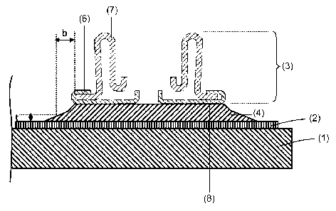
Fig.1 depicts a cross-section through a heatable pane 1 according to the
invention in the
region of the electrical connection element 3. The pane 1 is a 3-mm-thick
thermally
prestressed single-pane safety glass made of soda lime glass. The pane 1 has a
width of
150 cm and a height of 80 cm. An electrically conductive structure 2 in the
form of a
heating conductor structure 2 is printed on the pane 1. The electrically
conductive structure
2 contains silver particles and glass frits. In the edge region of the pane 1,
the electrically
conductive structure 2 is widened to a width of 10 mm and forms a contact
surface for the
electrical connection element 3. A covering screenprint (not shown) is also
situated in the
edge region of the pane 1. In the region of the contact surface 8 between the
electrical
connection element 3 and the electrically conductive structure 2, soldering
compound 4 is
applied, which effects a durable electrical and mechanical connection between
the
electrical connection element 3 and the electrically conductive structure 2.
The soldering
compound 4 contains 57 wt.-% bismuth, 40 wt.-% tin, and 3 wt.-% silver. The
soldering
compound 4 is arranged through a predefined volume and shape completely
between the
electrical connection element 3 and the electrically conductive structure 2.
The soldering
compound 4 has a thickness of 250 pm. The electrical connection element 3 is
made of
steel of the material number 1.4509 in accordance with EN 10 088-2
(ThyssenKrupp
Nirosta 4509) with a coefficient of thermal expansion of 10.0 x 10⁻⁶/ C. The
electrical
connection element 3 can have a silver coating (not shown), for example, with
a thickness
of roughly 5 p.m.
Steel of the material number 1.4509 in accordance with EN 10 088-2 has good
cold
forming properties and good welding properties with all methods except gas
welding. The
steel is used for construction of sound suppressor systems and exhaust gas
detoxification
systems and is particularly suited for that due to its scaling resistance to
more than 950 C
CA 02874689 2014-11-25
11
4351-11-28.878
and corrosion resistance against the stresses occurring in the exhaust gas
system.
However, other chromium-containing steels can be used for the connection
element 3. One
alternative particularly suitable steel is, for example, material number
1.4016 in accordance
with EN 10 088-2.
The electrical connection element 3 is implemented as a male snap. In the
embodiment
depicted, the electrical connection element 3 consists of a base plate 6 and a
connecting
element 7. In the plan view, the base plate 6 has a circular shape. The base
plate 6 has, in
the center, a circular hole, on the outer edge of which the base plate 6 is
bent upward such
that a region of the base plate extends away from the pane 1 roughly at a
right angle. The
outer edge of the base plate 6 bent in a U-shape. This forms a female seating
in the edge
region of the base plate 6 for the connecting element 7. The bent edge region
of the base
plate 6 can be designed continuous or discontinuous. The base plate 6, with
the exception
of the bent regions, is flat adjacent the hole and in the edge region. The
flat surface of the
base plate 6 facing the pane 1 forms the contact surface 8.
The base plate 6 has a material thickness of, for example, roughly 0.2 mm or
0.3 mm. The
circular outer edge of the base plate 6 has a diameter of, for example,
roughly 8 mm. The
circular hole in the center of the base plate 6 has a diameter of, for
example, roughly 1 mm.
The connecting element 7 is designed substantially as a hollow cylinder that
is arranged
substantially perpendicular to the surface of the pane 1. A foot region on the
outer edge of
the connecting element 7 is bent outward and extends roughly parallel to the
contact
surface 8 of the hollow cylinder. This foot region is inserted into the female
seating that is
formed by the bent region of the base plate 6. Thus, the connecting element 7
is durably
stably connected to the base plate 6 of the connection element 3. The walls of
the hollow
cylinder are realized by a roughly U-shaped bending of the connecting element
7, with the
radius of the U-shaped bend equaling, for example, roughly 0.3 mm. The hollow
cylinder
has an external diameter of, for example, roughly 5.7 mm and an internal
diameter of, for
example, roughly 3.5 mm. The material thickness of the connecting element 7
is, for
example, roughly 0.3 mm. The height of the connecting element 7 is, for
example, roughly
3.5 mm.
The connection element 3 is intended for and suitable for being connected to a
female
snap (not shown). For this purpose, the female snap is mounted on the
connecting element
CA 02874689 2014-11-25
12
4351-11-28.878
7. The outside wall of the hollow cylinder does not run perpendicular from the
pane 1, but,
instead, has an angle of, for example, roughly 3 relative to the
perpendicular such that the
diameter of the connecting element 7 becomes slightly larger with increasing
distance from
the pane 1. Thus, an unintentional slipping off of the mounted female snap is
avoided. The
female snap can, for example, include spring elements that exert pressure on
the outside
walls of the connecting element 7. A connection cable to the onboard
electrical system is
connected to the female snap. Thus, an electrical connection between the
electrically
conductive structure 2 and the external voltage source can be provided simply
and
conveniently.
The connecting element 7 can alternatively be provided, for example, with a
groove in
which a lip of the female snap engages upon mounting. If the diameter of the
connecting
element 7 becomes, at least in part of its height, larger with an increasing
distance from the
pane 1, the female snap can advantageously engage on the male snap, for
example, by
means of lips or spring elements.
Fig. 2 shows a cross-section through the connection element 3 of Fig. 1 in a
perspective
view. The connection element 3 includes the base plate 6 with the contact
surface 8 and
the connecting element 7.
Fig. 3 depicts in detail a method according to the invention for production of
a pane 1 with
an electrical connection element 3. An example of the method according to the
invention
for production of a pane with an electrical connection element 3 is presented
there. As a
first step, it is necessary to portion the soldering compound 4 according to
shape and
volume. The portioned soldering compound 4 is arranged on the contact surface
8 of the
electrical connection element 3. The soldering compound can, for example, be
formed as a
circular platelet that is arranged on the contact surface of the connection
element 3 of Fig.
1, with the hole in the center of the base plate 6 covered. The electrical
connection element
3 is arranged with the soldering compound 4 on the electrically conductive
structure 2. A
durable connecting of the electrical connection element 3 to the electrically
conductive
structure 2 and, thus, to the pane 1 takes place with the input of energy.
CA 02874689 2014-11-25
13
4351-11-28.878
Example
Test specimens were produced with the pane 1 (thickness 3 mm, width 150 cm,
and
height 80 cm), the electrically conductive structure 2 in the form of a
heating conductor
structure, the electrical connection element 3 according to Fig. 1, and the
soldering
compound 4. The connection element 3 was plated with silver. The soldering
compound 4
was applied in advance as a circular platelet with fixed layer thickness,
volume, and shape
on the contact surface 8 of the connection element 3. The connection element 3
was
applied with the soldering compound 4 applied on the electrically conductive
structure 2.
The connection element 3 was soldered onto the electrically conductive
structure 2 at a
temperature of 200 C and a processing time of 2 seconds. Outflow of the
soldering
compound 4 from the intermediate space between the electrical connection
element 3 and
the electrically conductive structure 2, which exceeded a layer thickness t of
50 pm, was
observed only to a maximum outflow width of b = 0.5 mm. The compositions of
the
electrical connection element 3 and the soldering compound 4 are found in
Table 1. No
critical mechanical stresses were observed in the pane 1 due to the
arrangement of the
soldering compound 4, predefined by the connection element 3 and the
electrically
conductive structure 2. The connection of the pane 1 to the electrical
connection element 3
via the electrically conductive structure 2 was durably stable.
With all specimens, it was possible to observe, with a temperature difference
from +80 C
to -30 C, that no glass substrate 1 broke or exhibited damage. It was
possible to
demonstrate that, shortly after soldering, these panes 1 with the soldered
connection
element 3 were stable against a sudden temperature drop.
CA 02874689 2014-11-25
14
4351-11-28.878
Table 1
Components Material Example
Connection element 3
Steel of material no. 1.4509 in accordance with
EN 10 088-2 with the composition:
Iron (wt.-%) 78.87
Carbon (wt.-%) 0.03
Chromium (wt.-%) 18.5
Titanium (wt.-%) 0.6
Niobium (wt.-%) 1
Manganese (wt.-%) 1
CTE (coefficient of thermal expansion) 10
(10-6/ C for 0 C ¨ 100 C)
Difference between CTE of the connection 1.7
element and substrate (10-6/0C for 0 C - 100 C)
Thermal conductivity (W/mK for 20 C) 25
Soldering compound 4
Tin (wt.-%) 40
Bismuth (wt.-%) 57
Silver (wt.-%) 3
Thickness of the solder layer in (m) 250 x 10-6
Glass substrate 1
(Soda lime glass)
CTE (10-6/ C for 0 C ¨ 320 C) 8.3
CA 02874689 2014-11-25
= 15
4351-11-28.878
Comparative Example
The comparative example was carried out the same as the example. The
difference
resided in the use of a different material for the connection element 3. The
connection
element 3 was 100 wt.-% titanium. The connection element 3 thus had lower
thermal
conductivity, a lower coefficient of thermal expansion, and a smaller
difference of the
coefficients of thermal expansion between connection element 3 and substrate
1. The
components of the electrical connection element 3 and the soldering compound 4
are
found in Table 2. The connection element 3 was soldered to the electrically
conductive
structure 2 in accordance with conventional methods by means of the soldering
compound
4. With the outflow of the soldering compound 4 from the intermediate space
between the
electrical connection element 3 and the electrically conductive structure 2,
which exceeded
a layer thickness t of 50 pm, an average outflow width b = 2 mm to 3 mm was
obtained.
The lower thermal conductivity of the material for the connection element 3
resulted, in the
comparative example, in a less uniform heating of the connection element
during the
soldering process.
With a sudden temperature difference from +80 C to -30 C, it was observed
that the glass
substrates 1 exhibited major damage shortly after soldering.
CA 02874689 2014-11-25
= 16
4351-11-28.878
Table 2
Components Material Comparative
example
Connection element 3
Titanium (wt.-%) 100
CTE (coefficient of thermal expansion) 8.80
(10-61 C for 0 C ¨100 C)
Difference between CTE of the connection 0.5
element and substrate (10-6/ C for 0 C - 100 C)
Thermal conductivity (W/mK for 20 C) 22
Soldering compound 4
Tin (wt.-%) 40
Bismuth (wt.-%) 57
Silver (wt.-%) 3
Thickness of the solder layer in (m) 250 x 10-6
Glass substrate 1
(Soda lime glass)
CTE (10-6/ C for 0 C ¨ 320 C) 8.3
The differences from Tables 1 and 2 above and the advantages of the connection
element
3 according to the invention are found in Table 3.
CA 02874689 2014-11-25
= 17
4351-11-28.878
Table 3
Embodiment according to the Comparative example
invention,
Example
Material Steel of material no. 1.4509 in Titanium
accordance with EN 10 088-2
Thermal conductivity 25 22
(W/mK for 20 C)
CTE (coefficient of 10 8.8
thermal expansion) of the
connection element
(10-61 C for 0 C ¨ 100 C)
Difference between CTE 1.7 0.5
of the connection element
and the substrate
(10-6/ C for 0 C - 100 C)
It was demonstrated that panes according to the invention with glass
substrates 1 and
electrical connection elements 3 according to the invention had better
stability against
sudden temperature differences. This result was unexpected and surprising for
the person
skilled in the art.
CA 02874689 2014-11-25
18
4351-11-28.878
List of Reference Characters
(1) pane
(2) electrically conductive structure
(3) electrical connection element
(4) soldering compound
(5) wetting layer
(6) base plate of the electrical connection element 3
(7) connecting element of the electrical connection element 3
(8) contact surface of the connection element 3 with the electrically
conductive
structure 2
b maximum outflow width of the soldering compound
t limiting thickness of the soldering compound