Note: Descriptions are shown in the official language in which they were submitted.
CA 02874899 2014-11-27
WO 2013/177665
PCT/CA2013/000232
- 1 -
TITLE: UNIVERSAL SYNCHRONIZATION ENGINE BASED ON
PROBABILISTIC METHODS FOR GUARANTEE OF LOCK IN
MULTIFORMAT AUDIO SYSTEMS
FIELD
[0001] The various embodiments described herein generally relate to
methods, devices and systems for synchronizing to a multiformat or unified
communication protocol.
BACKGROUND
[0002] In a computer or processor architecture, a bus is a subsystem
that transfers data between devices within an electronic device or transfers
data between electronic devices. Bus architectures are also used in common
data signalling paths for multiple devices rather than having separate
connections between each set of devices that may communicate with one
another. In other words, the bus structure can be used to allow one or more
slave devices to communicate with one or more master devices.
SUMMARY OF THE EMBODIMENTS
[0003] In one aspect, at least one embodiment described herein
provides a method of synchronizing a slave device to a master device that
communicates using a unified bus communication protocol having first and
second modes of operation. The method comprises assuming the first mode
of operation for the unified bus communication protocol; searching for a
synchronization pattern at one or more locations in transmitted data according
to the first mode of operation; obtaining synchronization when the located
synchronization pattern is verified according to at least one synchronization
rule for the mode of operation; and if synchronization is not obtained
assuming the first mode of operation, assuming the second mode of operation
for the unified bus communication protocol and carrying out the searching and
CA 02874899 2014-11-27
WO 2013/177665
PCT/CA2013/000232
- 2 -
obtaining acts on the transmitted data according to the second mode of
operation.
[0004] In at least one embodiment, the synchronization pattern
comprises a constant sync portion and a dynamic sync portion and the
searching act comprises searching for the constant sync portion.
[0005] In at least one embodiment, the constant sync portion is
different for the first and second modes of operation.
[0006] In at least one embodiment, the dynamic sync portion is
generated by a deterministic method such that the dynamic sync portions of
two consecutive synchronization patterns are different.
[0007] In at least one embodiment, the deterministic method employs a
Cyclic Redundancy Counter (CRC).
[0008] In at least one embodiment, the first mode of operation is
word
mode and the second mode of operation is bitstream mode or the first mode
of operation is bitstream mode and the second mode of operation is word
mode.
[0009] In at least one embodiment, when assuming word mode as the
mode of operation, the searching act is performed on the transmitted data for
various starting time slot positions up to and including a maximum frame
length unless the synchronization pattern has been located earlier.
[0010] In at least one embodiment, when assuming bitstream mode as
the mode of operation, the searching act is performed on the transmitted data
for various starting time slot positions up to and including a maximum frame
length and this is repeated for a maximum number of frame channels unless
the synchronization pattern has been located earlier.
[0011] In at least one embodiment, once the synchronization pattern
has been located, the searching and obtaining acts comprise searching for
the next synchronization pattern in order to determine a frame length that is
being used by the unified bus communication protocol.
CA 02874899 2014-11-27
WO 2013/177665
PCT/CA2013/000232
- 3 -
[0012] In at least one
embodiment, the at least one synchronization
rule comprises performing the searching and obtaining acts several times to
verify that the determined frame length is correct.
[0013] In at least one
embodiment, the searching and obtaining acts
comprise reading a current dynamic sync portion associated with a constant
sync portion that is located, the at least one synchronization rule comprises
calculating an expected dynamic sync portion based on the deterministic
method and the current dynamic sync portion, locating a next constant sync
portion and comparing a dynamic sync portion associated with the next
constant sync portion with the expected dynamic sync portion to reduce the
chance of false synchronization.
[0014] In at least one
embodiment, the at least one synchronization
rule comprises repeating the calculating, locating and comparing acts one or
more times to further reduce the chance of false synchronization.
[0015] In at least one
embodiment, the at least one synchronization
rule comprises adding a random component in the locating and obtaining acts
to improve the chances of synchronization under noisy conditions on bus
traffic.
[0016] In at least one
embodiment, the random component comprises
reading the parity of the
bus traffic for a certain period of time and using the
parity information to aid in determining whether the currently located
synchronization pattern is a true pattern or a false pattern.
[0017] In at least one
embodiment, the random component is used
when the synchronization pattern has been located under one or more errors.
[0018] In at least one
embodiment, the first mode of operation is
bitstream mode and clock gating is used to skip data from frame channels in
which bits of the synchronization pattern are not assumed to exist.
[0019] In at least one
embodiment, the method employs clock gating
and a common search structure for searching for the synchronization pattern
under both word mode and bitstream mode of operation.
CA 02874899 2014-11-27
WO 2013/177665
PCT/CA2013/000232
- 4 -
[0020] In at least one
embodiment, if the slave device falls out of
synchronization, the slave device assumes a frame length and a frame format
determined during previous a previous successful synchronization attempt
and attempts to regain synchronization.
[0021] In at least one
embodiment, if the dynamic sync portion
associated with the next constant sync portion does not match the expected
dynamic sync portion, the method further comprises continuing to search for a
constant sync portion with a dynamic sync portion that matches the expected
dynamic sync portion.
[0022] In at least one
embodiment, a limit is placed on how many
constant sync portions are searched for and located to locate the dynamic
sync portion that matches the expected dynamic sync portion.
[0023] In at least one
embodiment, if the limit is reached without finding
the match, the method further comprises selecting any of the located constant
sync portions as a valid sync portion.
[0024] in at least one
embodiment, after synchronization has been
achieved the method further comprises maintaining synchronization by
examining positions in the transmitted data that are in the vicinity of a
determined frame length's distance from a previous located synchronization
pattern.
[0025] In at least one
embodiment, the method further comprises
maintaining a current located constant sync portion regardless of not finding
a
match between an expected dynamic sync portion and an actual dynamic
sync portion until the searching exceeds a maximum frame length at which
point the current located constant sync portion is discarded and an ensuing
constant sync portion is used as the current located constant sync portion and
the search for the match is continued.
[0026] In at least one
embodiment, the method further comprises
generating a table of the dynamic sync portions corresponding to all valid
constant sync portions located within a maximum length of data, analyzing
CA 02874899 2014-11-27
WO 2013/177665
PCT/CA2013/000232
- 5 -
positions of the dynamic sync portions which match expected dynamic sync
portions for a repetition in separation between consecutive positions to
determine actual frame length, and using the actual frame length to obtain
synchronization.
[0027] In another aspect, at least one embodiment described herein
provides a method of synchronizing to a master device that communicates
using a unified bus communication protocol having first and second modes of
operation. The method comprises assuming the first and second modes of
operation for the unified bus communication protocol; concurrently searching
for a synchronization pattern at one or more locations in data transmitted
according to the first and second modes of operation; obtaining
synchronization when the located synchronization pattern is verified according
to at least one synchronization rule for one of the first and second modes of
operation; and if synchronization is not obtained, carrying out the searching
and obtaining acts according to the first and second modes of operation on
the transmitted data according to the unified bus communication protocol.
[0028] In at least one embodiment, the method may incorporate one or
more of the features described above for the various method embodiments.
[0029] In yet another aspect, at least one embodiment described
herein
provides a method of synchronizing a slave device to a master device that
communicates using a bitstream frame format. The method comprises
searching for a synchronization pattern at one or more locations in
transmitted
data according to the bitstream frame format; obtaining synchronization when
the located synchronization pattern is verified according to at least one
synchronization rule for the mode of operation; and if synchronization is not
obtained, repeatedly carrying out the searching and obtaining acts on newly
transmitted data, wherein in the bitstream frame format, the synchronization
pattern is multiplexed one bit at a time with other transmitted data.
[0030] In at least one embodiment, the method may incorporate one or
more of the features described above for the various method embodiments.
CA 02874899 2014-11-27
WO 2013/177665
PCT/CA2013/000232
- 6 -
[0031] In yet another aspect, at least one embodiment described herein
provides a method of synchronizing a slave device to a master device that
communicates using a word frame format. The method comprises searching
for a synchronization pattern at one or more locations in transmitted data
according to the word frame format; obtaining synchronization when the
located synchronization pattern is verified according to at least one
synchronization rule for the mode of operation; and if synchronization is not
obtained, repeatedly carrying out the searching and obtaining acts on newly
transmitted data, wherein in the word frame format, the synchronization
pattern is transmitted in consecutive bits in every frame of data.
[0032] In at least one embodiment, the method may incorporate one or
more of the features described above for the various method embodiments.
[0033] In yet another aspect, at least one embodiment described herein
provides an electronic device that communicates according to a unified bus
communication protocol having first and second modes of operation. The
device comprises an interface for sending and receiving signals; and a mux
and sync engine coupled to the interface, the mux and sync engine being
configured to synchronize the electronic device with a second electronic
device by assuming the first mode of operation for the unified bus
communication protocol; searching for a synchronization pattern at one or
more locations in transmitted data according to the first mode of operation;
obtaining synchronization when the located synchronization pattern is verified
according to at least one synchronization rule for the mode of operation; and
if
synchronization is not obtained assuming the first mode of operation,
assuming the second mode of operation for the unified bus communication
protocol and carrying out the searching and obtaining acts on the transmitted
data according to the second mode of operation, wherein the electronic
device is a slave device and the second electronic device is a master device.
[0034] In at least one embodiment, the device may incorporate one or
more of the features described above for the various method embodiments.
CA 02874899 2014-11-27
WO 2013/177665
PCT/CA2013/000232
=
- 7 -
[0035] In yet another aspect, at least one embodiment described
herein
provides an electronic device that communicates according to a unified bus
communication protocol having first and second modes of operation. The
device comprises an interface for sending and receiving signals; and a mux
and sync engine coupled to the interface, the =mux and sync engine being
configured to synchronize the electronic device with a second electronic
device by assuming the first and second modes of operation for the unified
bus communication protocol; concurrently searching for a synchronization
pattern at one or more locations in data transmitted according to the first
and
second modes of operation; obtaining synchronization when the located
synchronization pattern is verified according to at least one synchronization
rule for one of the first and second modes of operation; and if
synchronization
is not obtained, carrying out the searching and obtaining acts according to
the
first and second modes of operation on the transmitted data according to the
unified bus communication protocol, wherein the electronic device is a slave
device and the second electronic device is a master device.
[0036] In at least one embodiment, the device may incorporate one or
more of the features described above for the various method embodiments.
[0037] In yet another aspect, at least one embodiment described
herein
provides an electronic device that communicates according to a bitstream
frame format. The device comprises an interface for sending and receiving
signals; and a mux and sync engine coupled to the interface, the mux and
sync engine being configured to synchronize the electronic device with a
second electronic device by searching for a synchronization pattern at one or
more locations in transmitted data according to the bitstream frame format;
obtaining synchronization when the located synchronization pattern is verified
according to at least one synchronization rule for the mode of operation; and
if
synchronization is not obtained, repeatedly carrying out the searching and
obtaining acts on newly transmitted data, wherein in the bitstream frame
format, the synchronization pattern is multiplexed one bit at a time with
other
CA 02874899 2014-11-27
WO 2013/177665
PCT/CA2013/000232
- 8 -
transmitted data, and wherein the electronic device is a slave device and the
second electronic device is a master device.
[0038] In at least one embodiment, the device may incorporate one or
more of the features described above for the various method embodiments.
[0039] In yet another aspect, at least one embodiment described herein
provides an electronic device that communicates according to a word frame
format. The device comprises an interface for sending and receiving signals;
and a mux and sync engine coupled to the interface, the mux and sync engine
being configured to synchronize the electronic device with a second electronic
device by searching for a synchronization pattern at one or more locations in
transmitted data according to the word frame format; obtaining
synchronization when the located synchronization pattern is verified according
to at least one synchronization rule for the mode of operation; and if
synchronization is not obtained, repeatedly carrying out the searching and
obtaining acts on newly transmitted data, wherein in the word frame format,
the synchronization pattern is transmitted in consecutive bits in every frame
of
data, and wherein the electronic device is a slave device and the second
electronic device is a master device.
[0040] In at least one embodiment, the device may incorporate one or
more of the features described above for the various method embodiments.
[0041] In yet another aspect, at least one embodiment described herein
provides a computer readable medium comprising a plurality of instructions
executable on a microprocessor of a slave device for adapting the
microprocessor to implement a method of synchronizing the slave device to a
master device that communicates using a unified bus communication protocol
having first and second modes of operation, wherein the method comprises
assuming the first mode of operation for the unified bus communication
protocol; searching for a synchronization pattern at one or more locations in
transmitted data according to the first mode of operation; obtaining
synchronization when the located synchronization pattern is verified according
to at least one synchronization rule for the mode of operation; and if
CA 02874899 2014-11-27
WO 2013/177665
PCT/CA2013/000232
- 9 -
synchronization is not obtained assuming the first mode of operation,
assuming the second mode of operation for the unified bus communication
protocol and carrying out the searching and obtaining acts on the transmitted
data according to the second mode of operation.
[0042] In at least one embodiment, the computer readable medium
may incorporate one or more of the features described above for the various
method embodiments.
[0043] In yet another aspect, at least one embodiment described
herein
provides a computer readable medium comprising a plurality of instructions
executable on a microprocessor of a slave device for adapting the
microprocessor to implement a method of synchronizing the slave device to a
master device that communicates using a unified bus communication protocol
having first and second modes of operation, wherein the method comprises
assuming the first and second modes of operation for the unified bus
communication protocol; concurrently searching for a synchronization pattern
at one or more locations in data transmitted according to the first and second
modes of operation; obtaining synchronization when the located
synchronization pattern is verified according to at least one synchronization
rule for one of the first and second modes of operation; and if
synchronization
is not obtained, carrying out the searching and obtaining acts according to
the
first and second modes of operation on the transmitted data according to the
unified bus communication protocol.
[0044] In at least one embodiment, the computer readable medium
may incorporate one or more of the features described above for the various
method embodiments.
[0045] In yet another aspect, at least one embodiment described
herein
provides a computer readable medium comprising a plurality of instructions
executable on a microprocessor of a slave device for adapting the
microprocessor to implement a method of synchronizing the slave device to a
master device that communicates using a bitstream frame format, wherein the
method comprises: searching for a synchronization pattern at one or more
CA 02874899 2014-11-27
WO 2013/177665
PCT/CA2013/000232
- 1 0 -
locations in transmitted data according to the bitstream frame format;
obtaining synchronization when the located synchronization pattern is verified
according to at least one synchronization rule for the mode of operation; and
if
synchronization is not obtained, repeatedly carrying out the searching and
obtaining acts on newly transmitted data, wherein in the bitstream frame
format, the synchronization pattern is multiplexed one bit at a time with
other
transmitted data.
[0046] In at least one embodiment, the computer readable medium
may incorporate one or more of the features described above for the various
method embodiments.
[0047] In yet another aspect, at least one embodiment described
herein
provides a computer readable medium comprising a plurality of instructions
executable on a microprocessor of a slave device for adapting the
microprocessor to implement a method of synchronizing the slave device to a
master device that communicates using a word frame format, wherein the
method comprises: searching for a synchronization pattern at one or more
locations in transmitted data according to the word frame format; obtaining
synchronization when the located synchronization pattern is verified according
to at least one synchronization rule for the mode of operation; and if
synchronization is not obtained, repeatedly carrying out the searching and
obtaining acts on newly transmitted data, wherein in the word frame format,
the synchronization pattern is transmitted in consecutive bits in every frame
of
data.
[0048] In at least one embodiment, the computer readable medium
may incorporate one or more of the features described above for the various
method embodiments.
BRIEF DESCRIPTION OF THE DRAWINGS
[0049] For a better understanding of the various embodiments
described herein, and to show more clearly how these various embodiments
may be carried into effect, reference will be made, by way of example, to the
CA 02874899 2014-11-27
WO 2013/177665
PCT/CA2013/000232
-11 -
accompanying drawings which show at least one example embodiment, and
in which:
Figure 1 is a perspective view of a portable electronic device;
Figure 2 is a block diagram of a portion of the portable electronic
device;
Figure 3a is a schematic diagram of an example embodiment of
a bus system;
Figure 3b is a schematic diagram of the bus system of Figure 3a
showing an example of interface circuitry for coupling a master device to the
bus;
Figure 3c is a block diagram of an example embodiment of a
two-wire bus system;
Figure 4a is an example timing diagram of a transaction on the
bus in which a slave device writes "0110" on a single wire bus;
Figure 4b is an example timing diagram when the bus is
implemented using two wires;
Figure 5 is a diagram of an example embodiment of the fields
and bit allocations for a synchronization word;
Figure 6 is an example timing diagram showing data operations
to the data synchronization field of an S word in word mode;
Figure 7 is an example of the parity and acknowledgement
calculation that may be done by a master device and a slave device based on
different command operations;
Figure 8 shows various combinations of the command operation
(PING, READ, and WRITE), the value of the interrupt mask bit, the SO DELAY
bit and the action that should be taken;
CA 02874899 2014-11-27
WO 2013/177665
PCT/CA2013/000232
- 12 -
Figure 9a shows various fields and bit allocations for an
example embodiment of an X command word for various command
operations;
Figure 9b shows various fields and bit allocations for another
example embodiment of an X command word for various command
operations;
Figure 10 shows various fields and bit allocations for an
example embodiment of a Y command word for various command operations;
Figure 11a shows an example list of functions and
corresponding bit settings that may be set in the X word;
Figure 11b shows an example of encoding position information
in a device using two terminals using a fixed address and this configuration
is
also compatible with legacy systems;
Figure 11c shows an example of encoding position information
in a device using either a fixed address or a variable address O-N based on a
ring topology and this configuration is also compatible with legacy systems;
Figure 11d shows an example of the layout of a digital
microphone with a standard layout and full positional information;
Figure 11e shows an 10 cell that is capable of distinguishing
between GND, VDD and FLOAT conditions by using a weak output driver and
feedback;
Figure 12 shows an example of reading from a register after
activating a FUNCTION CAPABILITY to obtain capability information for a
master device or a slave device;
Figure 13 shows an example of the various data formats that
can be supported in an example embodiment of the unified bus
communication protocol;
Figure 14 shows an example of a status read from data registers
after the execution of the function READ LAST ERROR;
CA 02874899 2014-11-27
WO 2013/177665
PCT/CA2013/000232
- 13 -
Figure 15 shows an example of error codes that may be used
with an example embodiment of the unified bus communication protocol;
Figure 16a is an example of a definition of registers that can be
used for a master device or a slave device for an example embodiment of the
unified bus communication protocol;
Figure 16b is another example of a definition of registers that
can be used for a master device or a slave device for an example
embodiment of the unified bus communication protocol;
Figure 17 is an example of various power consumption levels or
power management modes that can be set for a port or a device in an
example embodiment of the unified bus communication protocol;
Figure 18 shows an example embodiment of a master device
that communicates with two slave devices using the unified bus
communication protocol and the devices have ports that are allocated to
various channels;
Figure 19 shows an example mapping between channels and
the CHANNEL SELECTION field that describes which channels of a port are
used for communication;
Figure 20 shows an example operation with regards to address
and bank selection during READ and WRITE operations;
Figure 21 shows an example of data from a single port being
repeated more than once in a frame in word mode;
Figure 22a shows an example of various field values that are set
depending on the use of isochronous, asynchronous and multi-frame transfers
in a given frame;
Figure 22b shows an example of a compressed format that can
be used to encode the PCLKD field of Figure 16a;
CA 02874899 2014-11-27
WO 2013/177665
PCT/CA2013/000232
- 14 -
Figure 22c shows an example of an alternative embodiment of
various field values that are set depending on the use of isochronous,
asynchronous and multi-frame transfers in a given frame;
Figure 23 shows an example of a frame format when using
multiple data channels with divisions between the channels from the same
port for achieving lower latency in word mode;
Figure 24 shows an example of a frame setup when data from
multiple data channels are repeated several times in a frame in word mode;
Figure 25a shows an example of the definition of the
COMMAND SEPARATION field depending on the frame type used in the
unified bus communication protocol;
Figure 25b shows an example definition of a number of
subframe lengths that can be used in bitstream mode to reduce the time for
synchronization;
Figure 25c shows an alternative example of the definition of the
COMMAND SEPARATION field depending on the frame type used in the
unified bus communication protocol;
Figures 26a and 26b show examples of different frame formats
that can be achieved by using different values for the HSTART and VSTART
fields in bitstream mode;
Figure 27 shows the definition of the LSB, MSB and LSB+1 bits
of the HSPACING and VSPACING fields for an example embodiment in
bitstream mode;
Figure 28a shows an example embodiment of a stereo system
with current and voltage sensing that uses the unified bus communication
protocol;
Figure 28b shows an example of a bitstream frame format that
can be used for the stereo system of Figure 28a;
CA 02874899 2014-11-27
WO 2013/177665
PCT/CA2013/000232
- 15 -
Figure 28c shows another example of a bitstream frame format
that can be used for the stereo system of Figure 28a and uses less bandwidth
for the sensing signals;
Figure 28d shows an example of a bitstream frame format that
can be achieved by setting values for the HSTART, VSTART, HSPACING
and VSPACING fields in bitstream mode where the bandwidth between the
audio data and the control data is changed so that less bandwidth is used on
the control data as compared to the audio data;
Figure 29a is an example embodiment of a definition of registers
that can be used for the master device;
Figure 29b is another example embodiment of a definition of
registers that can be used for the master device;
Figure 29c is an example of a definition of sampling ratios for a
first stage;
Figure 29d is an example of a definition of sampling ratios for an
optional stage;
Figure 29e is an example of a definition of sampling ratios for a
second stage;
Figure 29f is an example of a definition of sampling ratios for a
third stage;
Figure 29g is an example of a multiformat decimator system that
may be suitable for multiple sample rate ratios;
Figure 29h is an example of a multiformat interpolator system
that may be suitable for multiple sample rate ratios;
Figure 291 is an example of an interpretation of writing to the
FRAME CONTROL field;
Figure 30 shows combinations of WRITE and READ operations
based on the FRAME CONTROL field and example operations that can be
CA 02874899 2014-11-27
WO 2013/177665
PCT/CA2013/000232
- 16 -
monitored depending on the values of the FRAME CONTROL field in an
example embodiment;
Figure 31 shows combinations of WRITE and READ operations
based on the FRAME CONTROL field and example operations that can be
monitored depending on the values of the FRAME CONTROL field in another
example embodiment;
Figure 32a shows an example embodiment of the components
of an INTERFACE CONTROL register;
Figure 32b shows another example embodiment of the
components of the INTERFACE CONTROL register;
Figure 33a shows an example of how the MCLKD field can be
encoded in at least one example embodiment that corresponds to the register
definition of Figure 29a;
Figure 33b shows example frequency divisions that may be
used to generate a clock signal for the bus in at least one example
embodiment that corresponds to the register definition of Figure 29b;
Figure 34a shows an example embodiment of the subfields that
can be used in the IRQ MASK register;
Figure 34b shows another example embodiment of the subfields
that can be used in the IRQ MASK register;
Figure 35 shows an example timing diagram for changing the
FRAME DONE MASK field;
Figure 36a shows an example embodiment of the components
of an INTERFACE STATUS register;
Figure 36b shows another example embodiment of the
components of an INTERFACE STATUS register;
Figure 37 shows an example definition for the slave status
registers;
CA 02874899 2014-11-27
WO 2013/177665
PCT/CA2013/000232
- 17 -
Figure 38a shows an example embodiment of a compact
encoding format that can be used to encode a device ID for a slave device;
Figure 38b shows an example embodiment of a general
encoding format that can be used to encode a device ID for a slave device;
Figure 39 shows a general word frame format used in word
mode for a single time frame;
Figure 40 shows an example embodiment of a word frame
format for a single time frame;
Figure 41 shows another example embodiment of a word frame
format for a single time frame;
Figure 42 shows an example embodiment of a bitstream frame
format for a single time frame;
Figure 43 shows an example embodiment of a unified frame
format for a single time frame;
Figure 44 shows another example embodiment of a unified
frame format for a single time frame;
Figures 45a and 45b show tables of example combinations of
bus frequency, number and types of channels for the unified bus
communication protocol when operating in word mode;
Figures 46a and 46b show tables of example combinations of
bus frequency, number of channels and oversampling rate for the unified bus
communication protocol when operating in bitstream mode and using
bitstream frame formats;
Figure 47 shows a table of example combinations of bus
frequency, number and types of channels for the unified bus communication
protocol when operating in a hybrid word mode;
Figures 48a, 48b and 48c show tables of example combinations
of bus frequency, number and types of channels for the unified bus
CA 02874899 2014-11-27
WO 2013/177665
PCT/CA2013/000232
- 18 -
communication protocol when operating in bitstream mode and using unified
bitstream frame formats;
Figure 49a shows an example embodiment of a general format
for encoding N bits in digital word format in the unified bus communication
protocol;
Figure 49b shows an example of some common oversampling
factors that can be used with a bitstream encoding format for mobile phone
systems;
Figure 49c shows an example of possible combinations for a
string encoding format;
Figure 50a shows an example embodiment of an algorithm that
can be used to implement a fractional flow;
Figure 50b shows an example of the calculations of the
algorithm of Figure 50a for an example scenario;
Figure 50c shows an example of various values that can be
used for fractional flows for various playback scenarios;
Figure 51a shows an example embodiment of a control system
with a display that uses the unified bus communication protocol;
Figure 51b shows an example embodiment of a mobile phone
system that uses the unified bus communication protocol;
Figure 52a shows an example embodiment of a house safety
system that uses the unified bus communication protocol;
Figure 52b shows an example embodiment of a home
entertainment system that uses the unified bus communication protocol;
Figure 52c shows an example embodiment of a home
entertainment system that uses the unified bus communication protocol;
Figure 52d shows an example embodiment of an
instrumentation system that uses the unified bus communication protocol;
CA 02874899 2014-11-27
WO 2013/177665
PCT/CA2013/000232
- 19 -
Figure 52e shows an example embodiment of an electronic key
that that can communicate using the unified bus communication protocol;
Figure 52f shows an example embodiment of a memory stick
that can communicate using the unified bus communication protocol;
Figure 52g shows an example embodiment of a Subscriber
Identity Module (SIM) card that can communicate using the unified bus
communication protocol;
Figure 52h shows an example embodiment of an encrypted
credit card that can communicate using the unified bus communication
protocol;
Figure 521 shows an example embodiment of a heart rate
monitor system that uses the unified bus communication protocol;
Figure 53 shows an example embodiment of a method of
operating a bus according to the unified bus communication protocol;
Figure 54 is a diagram of an example embodiment of a universal
synchronization method;
Figures 55a and 55b are diagrams, respectively, of a first
scenario in which a true synchronization pattern is sent in the transmitted
data
and a second scenario in which true and false synchronization patterns are
sent in the transmitted data;
Figure 56 is a diagram of another example embodiment of a
universal synchronization method that utilizes a parallel implementation;
Figure 57 is a diagram of an example embodiment of a word
mode synchronization method that can be used with a universal
synchronization method;
Figure 58a is a diagram of an example embodiment of a method
that may be used to handle missing synchronization patterns and used with
the word mode synchronization method of Figure 57;
CA 02874899 2014-11-27
WO 2013/177665
PCT/CA2013/000232
- 20 -
Figure 58b is a diagram of an example embodiment of a method
that may be used with the method of Figure 57 to check if the current search
position exceeds the maximum length of a frame or a channel;
Figure 59 is a diagram of an example embodiment of a
bitstream mode synchronization method that can be used with a universal
synchronization method;
Figure 60 is a diagram of another example embodiment of a
universal synchronization method;
Figure 61a is a diagram of an example embodiment of another
method that can be used to check for missing synchronization patterns and
may be used with the universal synchronization method of Figure 60;
Figure 61b is a diagram of an example embodiment of a method
that can be used to check for frame overrun (i.e. the lack of synchronization
patterns for a longer time than is possible within a frame) and may be used
with the method of Figure 60;
Figure 62 is a diagram of another example embodiment of a
bitstream mode synchronization method that may be used with the universal
synchronization method of Figure 60;
Figure 63 is a diagram of an example embodiment of a
bitstream update method that may be used with the bitstream mode
synchronization method of Figure 62;
Figure 64 is a diagram of an example embodiment of a quick
resynchronization method;
Figure 65 is a diagram of an example embodiment of a clock
gating method that can be used with the universal synchronization method of
Figure 60;
Figure 66 shows an example of how the various embodiments of
the unified bus communication protocol can be used in wireless
communication;
CA 02874899 2014-11-27
WO 2013/177665
PCT/CA2013/000232
- 21 -
Figure 67 is a diagram of another example embodiment of the
fields and bit allocations for a synchronization word;
Figure 68 is another example timing diagram showing data
operations to the data synchronization field of the S word of Figure 67 in
word
mode;
Figure 69a is another example of a definition of registers that
can be used for a master device or a slave device for an example
embodiment of the unified bus communication protocol;
Figure 69b is an example showing various maximum channels
that can be used per subgroup;
Figure 69c is a diagram of an example embodiment of a system
having devices assigned to one device group address;
Figure 69d is a diagram of an example embodiment of a system
having devices assigned to three device group addresses;
Figure 70 shows another example list of functions and
corresponding bit settings that may be set in the X word;
Figure 71 is an example embodiment of a system that uses a
ring topology to couple devices to a bus and the system uses the unified bus
communication protocol;
Figure 72 is an example embodiment of a system that uses a
pipe topology to couple devices to a bus and the system uses the unified bus
communication protocol;
Figure 73 is an example embodiment of a system that uses pipe
control to couple many devices to a bus and the system uses the unified bus
communication protocol;
Figure 74 is an example embodiment of a system that uses a
single dimension, staggered ring topology to couple devices to a bus and the
system uses the unified bus communication protocol;
CA 02874899 2014-11-27
WO 2013/177665
PCT/CA2013/000232
- 22 -
Figure 75 is an example embodiment of a system that uses a
two-dimensional ring topology to couple devices to a bus and the system uses
the unified bus communication protocol;
Figure 76 is another example embodiment of a system that uses
pipe control to couple many devices to a bus and the system uses the unified
bus communication protocol;
Figure 77a is a timing diagram for an example of 2X overclocked
data slots;
Figure 77b is a table showing an example embodiment of timing
parameter values that may be used for devices that utilize overclocked data
slots;
Figure 77c is an illustration of data transfer and timing on a bus
for an example in which there is overclocking by a factor of two;
Figure 77d is a table of example settings for a register to
implement overclocking and an estimate of associated power savings;
Figure 78a shows a timing and voltage level scheme for sending
out multiple bits of data at a time;
Figure 78b is a table of example encoding that may be used
when a device sends out multiple packed bits in a data slot using the
overclocking mode;
Figure 79 is an example of data seen by a slave device during
the MASTER INITIATED DEVICE WAKE UP FROM SLEEP mode;
Figure 80a is an example of an alternative embodiment for
various power consumption levels or power management modes that can be
set for a port or a device using the unified bus communication protocol;
Figure 80b is a table of an example UART timing specification;
Fig 81a is an example of a single wire signaling system utilizing
two slots for synchronization and one for data;
CA 02874899 2014-11-27
WO 2013/177665
PCT/CA2013/000232
- 23 -
Fig 81b is an example of a single wire signaling system to
transfer both clock and data information utilizing two slots for
synchronization
and four slots for data; and
Fig 81c is an example of a single wire signaling system utilizing
one slot for synchronization and four slots for data thereby increasing the
bandwidth and lowering the power consumption.
DETAILED DESCRIPTION OF THE EMBODIMENTS
[0050] Various
systems or processes will be described below to provide
an example of one or more embodiments of the concepts. No embodiment
described below limits any of the claims and any of the claims' may cover
processes or systems that differ from those described below. The claimed
features are not limited to systems or processes having all of the features of
any one system or process described below or to features common to multiple
or all of the systems or processes described below. It is possible that a
system or process described below is not an embodiment that is recited in
any of the claims. Any concept disclosed in a system or process described
below that is not claimed in this document may be the subject matter of
another protective instrument, for example, a continuing patent application,
and the applicants, inventors or owners do not intend to abandon, disclaim or
dedicate to the public any such concept by its description in this document.
[0051]
Furthermore, it will be appreciated that for simplicity and clarity
of illustration, where considered appropriate, reference numerals may be
repeated among the figures to indicate corresponding or analogous elements.
In addition, numerous specific details are set forth in order to provide a
thorough understanding of the embodiments described herein. However, it
will be understood by those of ordinary skill in the art that the embodiments
described herein may be practiced without these specific details. In other
instances, well-known methods, procedures and components have not been
described in detail so as not to obscure the embodiments described herein.
CA 02874899 2014-11-27
WO 2013/177665
PCT/CA2013/000232
-24 -
Also, the description is not to be considered as limiting the scope of the
embodiments described herein.
[0052] It should also be noted that the term coupled as used herein
can
have several different meanings depending in the context in which the term is
used. For example, the term coupling can have a mechanical, electrical,
optical or communicative connotation. For example, in some contexts, the
term coupling indicates that two elements or devices can be physically
connected to one another or connected to one another through one or more
intermediate elements or devices via a physical or electrical element, such as
but not limited to a wire, a cable, a non-active circuit element (e.g.
resistor)
and the like, for example. In some contexts, the term coupling indicates that
two elements or devices can be connected through other means such as a
wireless signal or an optical signal. In some contexts, the term coupling
indicates that elements or devices may be communicatively connected to one
another through a signal, such as an electrical, optical or wireless signal,
for
example. Furthermore, the term "communicative coupling" indicates that an
element or device can electrically, optically, or wirelessly send data to
another
element or device as well as receive data from another element or device.
[0053] It should also be noted that the terms "master" and as "slave"
as
used herein are meant purely from a technological point of view and in
particular denotes the technical relationship between a host device or element
and a peripheral device or element in which one element or device provides
instructions or control signals to another element or device. Accordingly, the
use of the terms "master" and "slave" as used herein is not meant to carry any
connotation beyond the technical meaning given here.
[0054] It should also be noted that although the communication
protocol is described as a bus communication protocol and various example
embodiments are provided that show a physical bus that couples elements
together, the various embodiments of the communication protocol described
herein can also be implemented over a non-physical interface such as a
wireless or optical interface.
CA 02874899 2014-11-27
WO 2013/177665
PCT/CA2013/000232
- 25 -
[0055] It should
be noted that terms of degree such as "substantially",
"about", "approximate" and "approximately" as used herein mean a
reasonable amount of deviation of the modified term such that the end result
is not significantly changed. These terms of degree can be construed as
including a deviation of up to 10% of the modified term if this deviation
would
not negate the meaning of the term it modifies. Also, as used herein,
elements may be described as "configured to" or "adapted to" perform one or
more functions. In general, an element that is configured to or adapted to
perform a function is suitable for performing the function, or is operable to
perform the function, or is otherwise capable of performing the function.
Further, the word "current" may be used herein to mean "electrical current" (a
quantity measured in units of amperes), although there may be instances in
which the term refers to events occurring contemporarily or presently; the
meaning in a particular instance is generally clear from context.
[0056] Furthermore, in the following passages, different aspects of the
embodiments are defined in more detail. Each aspect so defined may be
combined with any other aspect or aspects unless clearly indicated to the
contrary. In
particular, any feature indicated as being preferred or
advantageous may be combined with at least one other feature or features
indicated as being preferred or advantageous. A feature or component that
may be preferred or advantageous is not necessarily essential.
[0057] The
detailed description begins with a general description of a
mobile device and then proceeds to describe example embodiments of a
unified bus communication protocol that can be used to couple devices with a
fewer number of wires while being able to support different types of data
formats. Accordingly, the unified bus communication protocol acts as a
unified interface for devices that generate numeric data in different formats
but can be coupled to the same bus.
[0058] The
unified bus communication protocol allows for
communication between at least two devices, such as between a master
device and a slave device, between two master devices, between two slave
CA 02874899 2014-11-27
WO 2013/177665
PCT/CA2013/000232
- 26 -
devices and between a master device and more than one slave device. The
data communication between the devices generally utilizes a continuous clock
unless otherwise specified and the communication can be bi-directional
unless otherwise specified.
[0059] The numeric data can
be audio data or measurement data such
as current, voltage, pressure, temperature and the like. The numeric data can
be initially produced by a device in a bitstream format or a digital word
format.
Digital words are meant to cover binary coded words, and floating point words
(i.e. unsigned or two's complement word).
[0060] In word mode, the
digital words can be transmitted along the
bus without being converted to another format. In bitstream mode, the data is
packaged using either a bitstream frame format or a unified frame format,
which is a type of bitstream frame format. In a bitstream frame format,
bitstreams are transmitted one bit at a time from different bitstream data
channels using frame channels. It should be noted that the term Pulse
Density Modulated data (PDM) data is sometimes used instead of the term
bitstream data.
[0061] The term data
channel generally refers to a channel that
generates or receives data in a certain format. Accordingly, a word data
channel comprises digital word data and a bitstream data channel comprises
bitstream data.
[0062] The term frame
channel is used to define channels of data in a
bitstream frame or a unified bitstream frame in which the frame channels are
multiplexed and are given certain time slots in a frame.
[0063] In a unified frame
format, there is at least one virtual frame
channel in which digital words for at least one word data channel are
converted to a bitstream and transmitted one bit at a time. In the unified
frame format, there may also be at least one bitstream frame channel which
receives bitstream data from one or more bitstream data channels. The
bitstream frame format and the unified frame format include a bitstream of
CA 02874899 2014-11-27
WO 2013/177665
PCT/CA2013/000232
- 27 -
command words in a control frame channel, which results in cost reduction
due the use of a reduced number of terminals. These frame formats will be
described in more detail later in this description.
[0064] Bitstream
data is data that is transmitted as a series of bits and
is sometimes referred to as pulse-density-modulated (PDM) data. They are
typically generated as the output of oversampled systems such as of delta-
sigma converters. The oversample rate is used to indicate the ratio between
a sampling clock and the final output sample rate after decimation (or vice-
versa for interpolation).
Bitstreams are used to transfer data in
telecommunication and audio applications and as a storage format (e.g. on
super audio CDs (SACD)).
[0065] A digital
word is a sequence of O's and l's having a certain
resolution that is used to represent an analog value in a digital format. For
example, a 16-bit digital word has 16 bits where each bit can be a 0 or a 1.
The digital word can be produced using a method called Pulse Code
Modulation (PCM) in which case the digital words are referred to as PCM
words or audio words (for audio applications). PCM words are used for digital
audio in a variety of devices including CDs, Blu-ray players, DVD players,
computers, smart phones, laptops, tablets and the like.
[0066] The data
that is communicated on the bus includes
synchronization data, control data, numeric data, and a clock signal. Power
can also be transmitted over the bus. The unified bus communication
protocol allows for a reduction in the number of wires that may be used for
the
bus and can be generally implemented on a single wire bus or a two wire bus,
as will be described in more detail. The single wire bus uses one wire to
transmit the synchronization data, control data, numeric data, clock signal
and
power. The two wire bus can use a first wire to transmit the synchronization
data, control data, numeric data, and power and a second wire to transmit the
clock signal. Accordingly, the bus and the associated unified bus
communication protocol may be used for operation where the number of pins
or wires is limited or where high reliability with respect to noise immunity
is
CA 02874899 2014-11-27
WO 2013/177665
PCT/CA2013/000232
- 28 -
desired. The bus and the associated unified bus communication protocol
described herein allow for continuous operation, unless otherwise stated, of a
variable number of devices that are all synchronized by the same clock signal
and discharge the bus at specified time instants, according to the frame
format, in order to provide a communication link. In embodiments where the
system clock frequency is low, one or more bus holders can be added to
maintain charge on the bus.
[0067] The second part of the detailed description provides various
example embodiments of synchronization methods that can be used by a
slave device to synchronize with a master device or with a bus which utilizes
at least one of the various embodiments of the unified bus communication
protocol described herein. The synchronization methods generally involve
techniques for searching for particular synchronization patterns, which is a
series of data bits (i.e. l's and O's) that may be ordered sequentially in
word
mode, or the bits of the synchronization patterns may be multiplexed or
interfaced with other data bits, although still transmitted in the same order,
in
bitstream mode.
[0068] In general, at least one of the synchronization methods may be
used to advantageously allow a slave device to attach to the bus after the bus
has been initialized and has been operating for some time. This is referred to
as hot plug in. Accordingly, the slave device can determine for itself what
mode of operation and frame format is being used for the bus communication
protocol without being told this information, which is advantageous and is
generally not done for conventional bus communication protocols.
[0069] In bus architectures, there is often a mechanism for devices to
signal when they need to use the bus, while it is in use, and the nature of
the
use, such as for numeric data and the transmission of command instructions,
for example. However, bus control can become quite complicated when
numerous asynchronous processes are attempting to share the bus efficiently
as well as when those processes use different data formats such as bitstream
data and digital word data. For example, in conventional bus systems,
CA 02874899 2014-11-27
WO 2013/177665
PCT/CA2013/000232
- 29 -
different interfaces are needed to support various kinds of data. As an
example, PCM interfaces support digital word data but not bitstream data and
bitstream interfaces do not support digital word data. There are often systems
that use both types of data since in some applications sensors use Nyquist-
type converters (e.g. temperature sensors, accelerometers, and displays) that
use binary words and in some applications bitstream interfaces are used for
low latency applications such as beamforming, active noise cancellation or
low latency control applications. Conventional bus systems use one interface
to communicate digital word data (such as a McBSP interface which requires
4 bus wires), another interface to communicate bitstream data (such as at
least one McPDM interface which requires another 4 bus wires) and another
interface for control data (such as I2C which requires another 2 bus wires)
for
a total of at least three interfaces and at least 10 bus wires and terminals.
This adds costs and extra space requirements for the components involved as
well as increased power consumption. Furthermore, when such systems are
used with external devices, multiple connectors are used resulting in larger
space requirements.
[0070] Accordingly, in at least one embodiment described herein, one
aspect of the unified bus communication protocol described herein is the
provision of a unified interface that can handle bitstream data, digital word
data and control data while using a smaller number of wires and therefore a
smaller number of terminals. The advantages of bitstream processing, such
as low latency and fast transient response, can be maintained by avoiding the
use of the digital word format. Therefore, an aspect of at least one
embodiment of the unified interface described herein is that bitstream data
can be multiplexed in order to achieve the same latency for bitstream
processing (i.e. one bit latency). Furthermore, digital word data can be
transmitted one bit a time with each bit being multiplexed with the bitstream
data, which eliminates the use of a digital word data interface. In addition,
control data, such as synchronization data and command data, can be
converted to a bitstream format and embedded as part of the multiplexed data
using the unified bus communication protocol, which eliminates the use of an
CA 02874899 2014-11-27
WO 2013/177665
PCT/CA2013/000232
- 30 -
extra interface (e.g. I2C) and also provides a robust programmable multiformat
data interface. Accordingly, an aspect of at least one embodiment of the
unified bus communication protocol includes support for tunneling
PCM/TDM/I2C streams and for transmitting bit streams with low latency.
[0071] Clock data can
also be incorporated into the control data (in a
one wire bus embodiment) or it can be provided using a separate wire (in a
two wire bus embodiment). Transmitting the clock signal on another wire
allows for the implementation of slave devices to be simplified and also
reduces the impact on clock jitter.
[0072] Accordingly,
the unified bus communication protocol can be
implemented using one or two wires depending on the specific requirements
of the system (e.g. as a headset interface or as a general bus system).
However, it should be noted that in alternative embodiments, the unified bus
communication protocol described herein can be used with buses having
more than two wires. Embodiments in which the bus uses more than one wire
can enable higher bandwidth and some simplifications in the physical layer.
[0073] In order
to multiplex the digital word data with the bitstream
data, in at least one embodiment described herein, one or more frame
channels in the unified interface can be allocated as virtual frame channels,
where the digital word data are multiplexed (i.e. interleaved or interlaced)
one
bit at a time along with the bitstream data while maintaining the proper order
of data for the data channels. There can also be embodiments in which there
are programmable combinations between frame channels that use bitstream
data and frame channels that use digital word data which allows for at least
one of bandwidth control and combining data that is sampled at different
sampling rates depending on the particular embodiment. A control channel is
also allocated in at least one embodiment of the unified interface so that the
control data can be multiplexed or interlaced one bit at a time along with the
other types of data.
[0074] In at least one
embodiment described herein, an aspect of the
unified bus communication protocol is the use of a varying frame length that
CA 02874899 2014-11-27
WO 2013/177665
PCT/CA2013/000232
- 31 -
makes it easier to support various clock frequencies and sample rates, such
as those that are commonly used in telecommunication applications (e.g. 19.2
and 13.0 MHz) for example, in a more efficient manner. Furthermore, the
unified bus communication protocol can accommodate other commonly used
frame lengths such as the frame length of 768 bits that is chosen for the
SLIMbus bus communication protocol and is suited for 12.288 MHz
applications. The control functionality that is provided by the unified bus
communication protocol has a wider functionality than the I2C bus
communication protocol and supports special functions such as those that are
used for audio in at least some embodiments, for example. At least one
embodiment of the unified bus communication protocol supports isochronous
transfer of bitstream data with low latency simultaneously with control data.
[0075] Furthermore, in at least one embodiment described herein, the
bus structure has a low complexity that is suitable for use in sensor
applications and audio applications, where a low gate count is advantageous
for integration, power consumption and economic reasons. A low gate count
can be achieved for both master and slave devices that use a sync engine
and associated hardware to communicate and synchronize according to the
various embodiments of the unified bus communication protocol described
herein. The lower gate count also results in lower driver complexity, smaller
silicon area and lower cost in Integrated Circuit (IC) implementations.
Furthermore, since the unified bus communication protocol is suited for I2C
tunneling, legacy systems can continue to be supported with little effort.
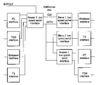
[0076] In at least one embodiment described herein, an aspect of the
unified bus communication protocol is the support for continuous monitoring of
the status of slave devices. This allows for hot plug-in and removal of slave
devices without any handshaking. This also allows slave devices to withdraw
themselves from the bus in case of errors in order to disturb the bus as
little
as possible. Accordingly, it is not possible for a slave device to stall the
bus
using the unified bus communication protocol which is not the case for the I2C
bus communication protocol. Furthermore, detection and correction of errors
CA 02874899 2014-11-27
WO 2013/177665
PCT/CA2013/000232
- 32 -
can be implemented much faster, in at least some embodiments of unified bus
communication protocol described herein, as compared to the SMbus
communication protocol. For example, SMbus can take about 35-40 ms
before detecting errors. The detection of a stalled bus is activated by the
internal time-out function (in case of no activity on the bus). This situation
can
be discovered much faster using at least one embodiments of the unified bus
communication protocol described herein. In some worst-case scenarios, it
might take the slave device about 50-100 ms to get back in synchronization
with the bus, but typically it would take about 1-10 ms for at least one
embodiment of the unified bus communication protocol described herein.
[0077] Referring now to Figure 1, shown therein is a perspective view
of a portable electronic device 10. In this example, the portable electronic
device 10 is a mobile communication device such as a cellular phone or a
smart phone. However, it should be understood that the embodiments
described herein are not limited to a phone but can be extended to any
electronic device that can benefit from a bus communication protocol that
provides a unified interface for different data formats. Examples of such
electronic devices generally include any portable electronic device such as
cellular phones wireless organizers, personal digital assistants, computers,
laptops, handheld wireless communication devices, wireless enabled
notebook computers, tablet computers or e-readers, electronic security
devices, wireless Internet appliances and the like. Other examples are
provided throughout this description. The electronic devices listed herein
which are mobile are generally portable and thus are battery-powered and
may have limited processing power, in which case it is beneficial to use a bus
communication protocol that provides a unified data interface, such as at
least
one of the embodiments of the unified bus communication protocol described
herein.
[0078] The portable electronic device 10 has a body 12 which includes
a display screen 14, a keyboard/keypad 16, a set of buttons 18 and a user
input device 20, such as a trackpad or a trackball. It will be understood that
CA 02874899 2014-11-27
WO 2013/177665
PCT/CA2013/000232
- 33 -
the user input device 20 is representative of a user-operated pointing or
input
device, which could also be presented as a joystick, scroll wheel, roller
wheel,
mouse or touchpad or the like, or another button. The portable electronic
device 10 includes other parts that are not shown or described because they
are well known to those skilled in the art. The portable electronic device 10
also includes at least one port for receiving a jack, but this is not shown in
Figure 1.
[0079] Referring now to Figure 2, shown therein is a block diagram of
a
portion of the portable electronic device 10. The portable electronic device
10
further includes a controller 30, which is connected to a chip 32, such as a
headset or headphone interface chip, which is integrated within the portable
electronic device 10. The controller 30 can be implemented using a
processor or dedicated circuitry. The chip 32 includes a switch matrix and
jack configuration detect portion 34 which is integrated with a port 36 for
receiving a jack 38 associated with a cable 40, such as a video cable or a
headset cable. The switch matrix 34 includes a plurality of individual input
and output ports 42 for receiving and transmitting signals with corresponding
wires or lines 44a to 44d within the jack 38.
[0080] The wires 44a to 44d within the jack 38 represent signal
lines,
such as audio and video lines. The set of individual lines, typically four,
although other jack configurations with other number of wires are
contemplated, allow for communication between the portable electronic
device 10 and a device located at the other end of the cable, such as a
headset. In one embodiment, the wires 44a and 44b can be a pair of audio
lines, the wire 44c can be a ground line and the wire 44d can be a
microphone line. However, only one of the lines is used for communication
and thereby serves as the communication bus for a single wire bus
embodiment. The remaining lines may be used for other functionality.
Typically, one line will be used for ground while the remaining two lines may
be used for headphone output. In another configuration, one line may be
used for bus communication, one may be used for ground, a third line may be
CA 02874899 2014-11-27
WO 2013/177665
PCT/CA2013/000232
- 34 -
used for power and the last line is left for other purposes such as a separate
clock line, for transmission of video signals or for other functionality. In
other
embodiments, a single wire bus may be used in digital or analog
transmissions between devices. Alternatively, a two wire bus embodiment is
useful for providing communication between two chips, as will be described in
more detail below.
[0081] Referring
now to Figure 3a, shown therein is a schematic
diagram of an example embodiment of a bus system 50. The bus system 50
includes a master device 52, such as a portable electronic device or a
headset interface chip within a portable electronic device, and a slave device
54, such as a headset. Although only one slave device 54 is shown, it will be
understood that multiple slave devices may be coupled to the bus system 50
for communication with the master device 52. Accordingly, the description
provided herein for the slave device 54 can be generally applied to other
slave
devices that are connected to the bus system 50.
[0082] The
master device 52 or the slave device 54 may include an
Inter-Integrated Circuit (I2C) interface 56 which is connected to a baseband
processor or other mobile processing unit. The master device 52 or slave
device 54 may also include an I2C interface for digital audio data. Inputs, or
input signals, 60 to the I2C interface 56 and a serial interface 58 may
include,
but are not limited to, an external clock signal 60a (EXT CLK), an I2C clock
signal 60b (I2C CLK) and an I2C data signal 60c (I2C DAT). An output of the
low speed serial interface 58 is connected to the slave device 54 via a cable
62, such as a co-axial cable. As described above, one of the wires or lines
within the cable 62 provides a bus 64 that is used for communication between
the slave device 54 and the master device 52 and can be seen as the single
wire bus. The bus 64 may be used where the number of pins or wires is
limited or for high reliability with respect to noise immunity. In other
embodiments, a two wire bus can be used.
[0083] In a single
wire bus embodiment, a single wire may combine
multiple functions, including, but not limited to, the transmission of both
clock
CA 02874899 2014-11-27
WO 2013/177665
PCT/CA2013/000232
- 35 -
and data in a single bus cycle. In operation, the I20 interface 56 retrieves
and
sends data to the slave device 54 over the bus 64. In other embodiments,
communication over the bus 64 may be controlled via a connection to a
baseband processor or another processing unit. Accordingly, control of the
master device 52 can be via the I2C interface 56, through another control
interface or as part of a connection to the baseband processor or other
processing unit that has the master device 52 perform various operations
such as, but not limited to, PING, READ, WRITE and FUNCTION commands
or operations. In at least one embodiment described herein, the PING,
READ, WRITE and FUNCTION commands many not occur in the same frame
since each frame is defined by only one operation. These operations will be
described in more detail throughout the description.
[0084] The master device 52 generates framing information in order to
allow the slave device 54, or multiple slave devices, to be synchronized to
the
bus 64. In one embodiment, the frame length is determined by an 8-bit
register that provides a separation distance between the start of each block
of
command data. In another embodiment, the unit of measure is a nibble which
equals four (4) bits. The frame length is determined by the command pattern
and in one embodiment, in word mode, may be 48 bits with a default sync
separation value of 28 nibbles thereby resulting in a frame length of 384
bits.
[0085] In operation, a synchronization (sync) signal, control signals
of
information, data, a clock signal and power is transmitted between the master
device 52 and the slave device 54 over the bus 64. Accordingly, the bus 64
allows continuous operation of a number of external devices and all devices
are synchronized by the same clock signal. The clock signal can be used as
a sampling clock for internal circuits such as sigma-delta converters or for
continuous operation of a complex logic circuit. In other embodiments, there
may be instances in which the clock signal is kept at a steady level such as
static low logic level or a static high logic level to save power when there
is no
activity on the bus 64 as will be explained in more detail below.
CA 02874899 2014-11-27
WO 2013/177665
PCT/CA2013/000232
- 36 -
[0086] The size
of components that communicate via the bus 64 may
be decreased by using at least one embodiment of the unified bus
communication protocol described herein. For example, if implemented in the
portable electronic device 10 of Figure 2, the unified bus communication
protocol allows the bus 64 to transmit the clock signal and the data over a
single wire which reduces the number of pins that are occupied in the chip 32
thereby allowing the other pin ports 42 to be used for other functionality or
to
reduce the total pin-count, silicon area or cost of the chip at the Printed
Circuit
Board (PCB) level.
[0087] Referring now
to Figure 3b, shown therein is a schematic
diagram of the bus system 50 showing an example of interface circuitry 70 for
coupling the master device 52 to the bus 64. This schematic is primary for the
single wire version of the bus, but could also be used for the data line in
the
two wire version. Similar circuitry can be used to couple the slave device 54
to the bus 64. The interface circuitry 70 includes a charge transistor 72, a
discharge transistor 74, a power transistor 76 and a resistor R1. The charge
transistor 72 is used to assert a logic "1" on the bus 64 and the discharge
transistor 74 is used to assert a logic "0" on the bus 64. The power
transistor
may be used to charge a slave device quickly (e.g. a battery) when more
current is used than the current that is normally provided through the series
termination resistor R1. With this arrangement, the bus 64 does not suffer
from time-constrained implementations such as open-collector and open-drain
types, where the signaling speed is a compromise between power
consumption, noise immunity and bandwidth. The power transistor 76 is
optional and may be included in some embodiments for charging devices and
powering external devices when there is no communication. The power
transistor 76 may be controlled by a register and updated at the beginning of
a frame.
[0088] The charge
transistor 72 and the power transistor 76 are PMOS
transistors while the discharge transistor 74 is an NMOS transistor, in this
particular example embodiment. A source node of the charge transistor 72 is
CA 02874899 2014-11-27
WO 2013/177665
PCT/CA2013/000232
- 37 -
coupled to the supply voltage VSS, a gate node of the charge transistor 72 is
coupled to a first pin of the low speed serial interface 58 and a drain node
of
the charge transistor 72 is coupled to a drain node of the discharge
transistor
74. The gate node of the discharge transistor 74 is coupled to a second pin of
the low speed serial interface 58 and the drain node of the discharge
transistor 74 is coupled to ground. The gate node of the power transistor 76
is coupled to a third pin of the low speed serial interface 58, the drain node
of
the power transistor 76 is coupled to the supply voltage VSS and the source
node of the power transistor 76 is coupled to a fourth pin of the low speed
serial interface 58 and a first node of the bus 64. One node of the resistor
R1
is coupled to the source node of the charge transistor 72 and the source node
of the discharge transistor 74 and a second node of the resistor R1 is coupled
to the first node of the bus 64. In an example embodiment, the resistance of
resistor R1 can be selected such that the output resistance of the interface
circuitry 70 is generally about 75 Ohms and the supply voltage VSS may be
3V.
[0089] The node
of the low speed serial interface 58 connected to the
charge transistor 72 applies a low voltage so that the charge transistor 72
may charge the bus 64 at the start of every bus cycle. After that, the bus 64
is
left floating by deactivating the charge transistor 72. The master device 52
may then drive the bus 64 by activating the discharge transistor 74 by
applying a high voltage to its gate, which will discharge the bus 64. The
connection to the bus 64 after the resistor R1 is used to receive data from
the
bus 64 (in some cases, a delay may be included for improved setup/hold
timing margins). The node of the low speed serial interface 58 that is coupled
to the power transistor 76 is used to supply larger power to the bus 64 than
is
available through the resistor R1. This may lead to some initial ringing,
unless
certain actions are taken, such as first applying the full power after the
transistor 72 has been activated (this will decrease the ringing).
[0090] In one
embodiment, the bus 64 is implemented using a low-
high-float cyclic pattern but may alternatively be implemented as a high-low-
CA 02874899 2014-11-27
WO 2013/177665
PCT/CA2013/000232
- 38 -
float pattern. The actual transfer of data occurs during the floating period,
while the low-high (or high-low) period is used to transfer power and for
clock
synchronization. If the slave device 54 or the master device 52 wants to
signal a logic zero, that particular device will leave the bus 64 in the same
state as before, i.e. floating and with the same value on the bus 64. The
slave
device 54 or the master device 52 may signal a logic one by discharging the
bus 64 during the floating period thereby changing the state of the bus 64 to
the opposite logic level. An example of the signalling scheme is shown in
Figure 4a which shows a timing diagram of a transaction on the bus 64 in
which the slave device 54 writes "0110". The external clock signal is
typically
provided to the master device 52 (in alternative cases, the master device 52
may generate a clock signal). When the master device 52 or the slave device
54 goes into tri-state mode, this has been drawn as a dashed line in Figure 4a
for illustrative purposes. In practice, the output voltage will be determined
by
the remaining charge left on the bus 64. However, once the bus 64 has been
discharged, there will be no more changes no matter how many devices try to
attempt this discharge. This signalling scheme therefore allows for the
reduction or avoidance of bus contention, or congestion, when multiple
devices try to signal, or communicate over the bus 64, at the same time, since
once the bus 64 has been discharged, the discharge of the bus 64 by
subsequent devices is not detected and bus collision is not possible.
[0091] As can be seen by the example in Figure 4a, timing is
implemented on the bus 64 such that the bus 64 is time-multiplexed in four
time intervals. In alternative embodiments, it may be possible to use another
number of time intervals. For the example of Figure 4a, in a first time
interval,
the master device 52 drives the bus 64 active low during the first 25% (i.e.
quarter) of the clock period. In a second time interval, the master device 52
drives the bus 64 active high during the second 25% of the clock period. The
low-high clock transition may be used as a continuous sampling clock signal.
In the third and fourth time intervals, the master device 52 leaves the bus 64
in a floating state for the remainder of the clock period unless the slave
device
54 or the master device 52 pulls the bus low to signal a "1". For example, in
CA 02874899 2014-11-27
WO 2013/177665
PCT/CA2013/000232
- 39 -
the third interval the slave device 54 may pull the bus 64 active low, for
example, starting between 50-62% of the clock period. The bus 64 may
typically be fully settled before the clock period is complete. The bus value
is
sampled in the fourth interval near the end of the clock period, for example,
at
88-100% of the clock period, after which the master device 52 will begin to
drive the bus 64 active low again. In one embodiment, the first half of the
clock cycle may be used for the clock signal while the second half of the
clock
cycle may be used for the data transmission. However, other divisions of the
clock cycle are contemplated in which a first percentage of the clock cycle is
used for the clock signal and a second percentage of the clock cycle is used
for data transmission, such as 67% for the clock signal and then 33% for the
data transmission, for example.
[0092] In the example of Figure 4a, the bus 64 is initially active
low at
the beginning of the clock cycle. After a particular period of time, the bus
64
is driven active high by the master device 52. As the slave device 54 wishes
to transmit a "0", the slave device 54 does not do anything with the bus 64.
The value of "0" is then read by the master device 52 and the slave device 54
before the master device 52 drives the bus 64 to an active low prior to the
next clock cycle. During the second clock cycle, the master device 52 drives
the bus 64 to an active high after a particular period of time. As the slave
device 54 wishes to transmit a "1", the slave device 54 pulls or drives the
bus
64 to an active low where the value is then read by the master device 52 and
the slave device 54. As the bus 64 is active low, the master device 52 does
not have to drive the bus 64 active low, although it may perform that function
as shown in Figure 4a. In the third clock cycle, after a particular period of
time, the master device 52 drives the bus 64 to an active high. As the slave
device 54 wishes to transmit a "1", the slave device 54 pulls or drives the
bus
64 to an active low where the value is then read by the master device 52 and
the slave device 54. At the start of the fourth clock cycle, the bus 64 is
active
low and after a particular period of time is driven active high by the master
device 52. As the slave device 54 wishes to transmit a "0", there is no
activity
CA 02874899 2014-11-27
WO 2013/177665
PCT/CA2013/000232
- 40 -
on the bus 64 until after the value has been read and then the master device
52 drives the bus 64 active low in preparation for the next clock cycle.
[0093] The bus timing allows for the slave device 54 to continue to
pull
the bus 64 active low during the period where the master device 52 drives the
bus 64 active low. Therefore, the release timing of an output driver of the
slave device 54 is not so stringent. However, the slave device 54 generates a
floating output when the master device 52 drives the bus 64 active high,
including line delays. The reason the floating period is longer than the
active
low period and the active high period is to allow the slave device 54 to drive
the bus 64 active low in the same amount of time as the master device 52,
and allow some tolerance to the time instant, when the activation starts,
since
the slave device 54 depends on the timing of the master device 52.
Furthermore, there are delays on the bus 64.
[0094] The timing of when the bus 64 is pulled low by the master
device 52 is after a particular period of time so that incorrect data is not
sampled by the master device 52 or the slave device 54. Accordingly, the
slave device 54 has a floating output when the master device 52 pulls the bus
64 high.
[0095] When the master device 52 or the slave device 54 enters the
tri-
state, this is represented by dashed lines even though the actual voltage will
be determined by the previous values written to the bus 64. As the period
during which the bus 64 floats is very short, it may be kept stable due to
parasitic capacitances coupled to the bus 64 or may be kept stable for longer
periods of time by including at least one bus holder within the system 50.
Therefore, the charge and the voltage on the bus 64 may be considered
stable, if unloaded statically or loaded by high impedance.
[0096] The slave device 54 activates the bus 64 at certain time
intervals, which can be done by implementing a local clock, using a PLL, a
Delay Locked Loop (DLL) or a simple delay circuit. The delay circuit may
comprise two capacitors that are being alternately charged by a fixed current
and then using the charging voltage on the capacitors to determine the points
CA 02874899 2014-11-27
WO 2013/177665 PCT/CA2013/000232
- 41 -
where the bus 64 should be activated and sampled. These two capacitors
may be charged from one fixed clock edge to the next fixed clock edge and
discharged before starting this cycle. During long periods where information
is not transferred, it is possible to let the bus 64 go idle by gating the
clock
signal to a high level. In this case, there will be a small delay in order to
restart the bus 64. Since the master device 52 controls the timing, any analog
controlled delays are generally not used.
[0097] In general, a small enough bus capacitance and a clock
frequency that is sufficiently high is used so that the reading of the status
of
the bus 64 during the floating, or tri-state, period is uniquely defined. If
the
bus system 50 is implemented on a printed circuit board, in some
embodiments, a small capacitor may be used to provide a significantly large
charge to protect against data errors. In this case, a small but finite bus
capacitance is used or alternatively implemented using a bus holder (e.g.
using two inverters coupled back-to-back) to maintain a stable bus value.
This method may be chosen for low frequency operation of the bus 64, where
small leakage currents may slowly discharge any charges left on the bus 64,
but a bus holder will keep the value stable. The bus holder will normally be
implemented in the master device 52 to limit the power efficiency loss
associated with its operation but can also be implemented in the slave device
54 for data integrity purposes. The timing characteristics for an example
embodiment of when the bus 64 is implemented using a single wire are
shown in Table 1.
Table 1: An Example of Timing Characteristics for a Single Wire Bus
PARAMETER MIN NOM MAX
UNIT
Bus frequency (1.8 m cable) =
1 6 12 MHz
EXTCLK/divider
Duty cycle clock 45 50 55
Setup time (slave device) 5 ns
Hold time (slave device) 5 ns
Slew rate (master device), charge VDD*0.1 VDD*0.5 V/ns
Slew rate, discharge VDD*0.1 VDD*0.5 V/ns
CA 02874899 2014-11-27
WO 2013/177665 PCT/CA2013/000232
= - 42 -
[0098] An
estimation of the maximum disturbance on the bus 64, if a
lower clock frequency of 2 MHz is used (normally a 6 MHz clock frequency is
recommended) can be made. Assuming a maximum leakage current of 10
pA, a period of 1 ps and a line capacitance of 100 pF, the maximum voltage
drop is equal to about 0.05 V. When the clock frequency is increased further,
the noise immunity increases. The output impedance of the master device 52
is about 75 12 Q to match to a 75 CI transmission line. When received at the
end of the transmission line, the reflection will immediately bring the
voltage
up to the full level with little impact on the slew-rate. With
these
characteristics, the noise immunity will be better than that of an I2C type
implementation. For a 2 meter long cable, an estimate of the cable delay is
about 10 ns (delay approximately 20 cm/ns). The use of a 75 Ohm cable to
implement the bus 64 has the advantage of lower capacitance per length than
a 50 Ohm cable and lower electrical losses. The electrical characteristics for
an example embodiment of the bus 64 when using a single wire is shown in
Table 2.
Table 2: An Example of Electrical Characteristics for a Single Wire Bus
PARAMETER MIN NOM MAX UNIT
VDD 1.62 1.98 Volt
VL, in 0.65 Volt
VH, in 1.40 Volt
!load (bus stopped, sync off, power
transistor on), Vdrop = 300 mV 30 mA
(POWER MODE)
Bus holder output impedance
600 1200 1800
(master device)
Slew-rate limit (at master device)
0.3 0.6 1.0 V/ns
with 75 pF load or smaller
Output impedance of driver 63 75 87 CI
[0099] When implementing
the unified bus communication protocol on
a bus having a two wire implementation, the clock and data information can
be transmitted on separate wires (i.e. a clock line and a data line). In this
case a delay circuit may not be used inside the slave device 54 and internal
CA 02874899 2014-11-27
WO 2013/177665
PCT/CA2013/000232
- 43 -
timing circuits that use both clock edges will have better jitter performance.
This bus structure is suited for implementation on a PCB where the pin
requirement is less strict. In an embodiment, the method used to signal can
be NRZI signaling, i.e. a logic zero is signaled by maintaining the level on
the
bus 64, while a logic one is signaled by changing the level on the bus 64.
[00100] Referring now to Figure 3c, shown therein is an example
embodiment of a two wire bus system. In this example, the master device 1 is
coupled to an I2C interface, a TDM interface, a bitstream interface, and an
I2S
interface through a low speed serial interface. The master device 1 is then
coupled to a slave device 1, a slave device 2 and a master device 2 via a two-
wire bus that may operate according to at least one of embodiments of the
unified bus communication protocol described herein. The two-wire bus has a
first wire that carries clock information and a second wire that carries data,
synchronization and command information. In this example, each of the slave
devices 1 and 2 and the master device 2 is coupled to the bus via a low speed
serial interface. The slave device 1 is also coupled to a second bitstream
interface. The slave device 2 is also coupled to a second I2S interface. The
master device 2 is also coupled to a second I2C interface and a second TDM
interface.
[00101] When a two-wire bus with separate clock and data lines is used,
the clock signal will merely provide timing information on when the
information
as signaled on the DATA line is valid or not. In some cases, information may
be transferred on a single clock edge or on both clock edges. In some cases,
information on the DATA line may change more than twice within a single
clock cycle in order to reduce power consumption of the clock line.
[00102] Referring now to Figure 4b, shown therein is an example timing
diagram when the bus 64 is implemented using two wires. When using the
protocol with two wires, it is possible to either transfer data on one clock
edge
only (either rising or falling) or on both clock edges. The advantage of using
both clock edges is that it allows for higher bandwidth and lower current
consumption. However, there are constraints on the bus radius once the
CA 02874899 2014-11-27
WO 2013/177665
PCT/CA2013/000232
- 44 -
physical characteristics of the interface have been chosen. If only one clock
edge is used, it is possible to use a very long bus radius, as long as the
clock
frequency is reduced. However, when two clock edges are used a slave
device that is located close to the master device 52 may begin to output data
before they have been sampled from a slave device that is located further
away from the master device 52. One way to solve this problem is to ensure
that the time before the data are enabled on the bus 64 for a device that has
been tri-stated in the previous data slot is longer than the time it takes for
a
device to go from the data state to the tri-state. Furthermore, the timing
margins may be improved by delaying the output clocking of data to the bus
64 a little bit while the data are clocked in from the bus 64 immediately on
the
clock edges. In some embodiments, the timing margin may be adjusted to
depend on the clock frequency in order to enable operation either at high
frequency or with a large bus diameter. As an example, the data could be
kept stable for a longer time after a clock transition for a lower frequency
of
operation. In other cases, it may be decided to use fixed parameters for the
timing margin and use bitstream mode with every second channel empty
(effectively tri-stated) for systems with a large bus radius to avoid problems
when two slave devices receive the clock signal at different times, which
could
result in one slave device located close to the master device 52 overwriting
the result from a slave device located far away from the master device 52. In
alternative embodiments, different structures can be used for connecting the
slave devices 54 to the bus 64 such as a ring structure or a pipe structure,
for
example. These structures are described in more detail with respect to
Figures 71 to 76. In some embodiments, the master device 52 may contain a
direct connection to a pipe or ring structure; in other embodiments a hub
device may act as the interface between a one-wire or two-wire multiple-drop
bus and the alternate pipe or ring topology.
[00103] This implementation of a 2 wire bus reduces power consumption
as compared to an I2C implementation and similar open-collector structure
implementations and does not infer a compromise between bandwidth and
power consumption as is the case with the I2C and similar open-collector
CA 02874899 2014-11-27
WO 2013/177665
PCT/CA2013/000232
- 45 -
structure implementations. In some cases, a two wire embodiment of the bus
64 which uses the unified bus communication protocol results in a 40% lower
power consumption than SLIMbus and double the bandwidth. Furthermore, in
some embodiments, the same physical layer as is used in SLIMbus can be
used to implement the unified bus communication protocol.
[00104] In at
least some embodiments, a bus holder can be
implemented in the master device 52. This
gives predictable noise
performance in situations where there are few and many slave devices.
When no power is applied to a device connected to the bus 64, it should still
be possible to operate the bus 64 even though the device with no power is
still
connected to the bus 64, e.g. (Electro-Static Discharge) ESD structures
should not stall the bus 64 when no power is applied. The electrical
characteristics for an example embodiment of the bus 64 when using two
wires are shown in Table 3.
Table 3: An Example of Electrical Characteristics for a Two-Wire Bus
PARAMETER MIN NOM MAX
UNIT
Bus frequency (0.30 cm PCB) =
0 10 20 MHz
EXTCLK/divider
Clock half period (high or low but
23 ns
not both)
Setup time 2 ns
Hold time 2 ns
Bus holder (master device only) 600 1200 1800 Ohm
Slew rate VDD*0.1 VDD*0.5 V/ns
Time to disable output, TD-z 5 ns
Time to enable output, TZ-D 6 12 ns
Internal delay on data line before
1 2 3 ns
sampling
[00105] Regarding
power consumption, if it is assumed that data
changes on one clock edge for the two wire bus embodiment, dynamic power
consumption due to capacitive charging will be lower for the single wire bus
embodiment as compared to the two wire bus embodiment. The state
changes used per transmitted bit will be two for the single wire bus
CA 02874899 2014-11-27
WO 2013/177665 PCT/CA2013/000232
- 46 -
embodiment (i.e. a signal going up and down), while the two wire bus
embodiment will on average use 21/2 signal changes due to the clock signal
going up and down and the data signal on average changing every second
time. The single wire bus embodiment allows additional data information to
be carried in the clock signal without any extra power consumption (i.e. no
extra charging of the lines), since the signal may be duty cycle modulated.
This is an example of when the clock and data lines are combined into a
single line in order to reduce the number of terminals and to reduce power
consumption by reducing the number of signal transitions. In other
embodiments, the single wire bus may also be level modulated in order to
transfer more bits per clock cycle. However, if data changes on both clock
edges of the two wire bus embodiment, then it will be more power efficient
since the two wire bus embodiment will only use 11/2 state changes for every
bit transmitted, i.e. one clock change and an average of a IA data signal
change.
[00106] It should be noted
that it should be more efficient in terms of
power, to have as few devices as possible connected to the bus 64, since the
power efficiency degrades linearly with the number of devices attached to the
bus 64. If multiple devices may be attached to a single bus line, it is
advantageous to reduce the input capacitance of each device to lower the
resulting power consumption. Alternatively, there can be embodiments in
which more than one bus is used so that some of the devices are coupled to
one bus and other devices are coupled to another bus and there is a device
that is common to both buses, such as a master device.
[00107] In general, the slave
device 54 can indicate that it wishes to
communicate with the master device 52 by actively pulling the signal down
during a PING operation. In this case, data can then be transmitted between
the slave device 54 and the master device 52 via a READ, WRITE or
FUNCTION operation. The master device 52 can also initiate a READ,
WRITE or FUNCTION operation on its own. In order to initiate the
CA 02874899 2014-11-27
WO 2013/177665
PCT/CA2013/000232
- 47 -
communication, the master device 52 and the slave device 54 are
synchronized to each other as described in more detail below.
[00108] In an example embodiment of the unified bus communication
protocol, a frame is defined to include three control words: a synchronization
word (i.e. the S word) and two command words (i.e. the X word and the Y
word) for communicating commands to and from the slave devices. The
control words may be 16 bits long and are generally sent out during every
frame. In other embodiments, the length of the control words may be some
other length, e.g. 8 bits and the number of control words in a frame may
differ
from three. However, the control words can be transmitted differently during a
frame depending on the mode of operation: e.g. a word mode and a bitstream
mode. For example, in word mode, the distance between the control words
can vary which enables support of different oversample ratios and clock
frequencies. In the bitstream mode, data bits are interleaved between the
individual bits in each control word; one benefit of this data interleaving is
the
support of multiple low latency bitstream data channels.
[00109] In an example embodiment, the master device 52 performs
several control functions including: status monitoring (i.e. a PING
operation),
reading a register (i.e. a READ operation), writing to a register (i.e. a
WRITE
operation) and executing functions (i.e. a FUNCTION operation). The type of
operation is determined by the master device 52. In some embodiments, the
master device 52 is controlled by a system controller (not shown). In these
cases, the interface between the master device 52 and the system controller
can be implemented using an I2C bus or by integrating these two system
components into one device (i.e. a processor).
[00110] In order to communicate with the slave device 54, the master
device 52 transmits a synchronization (i.e. sync or S) word that has
synchronization data that the slave device 54 (or devices) may use to
synchronize their internal timing, or clock, with the master device 52 and
consequently the bus 64 as well. In general, the first control word that the
master device 52 transmits in a frame is the S word. Accordingly, the S word
CA 02874899 2014-11-27
WO 2013/177665
PCT/CA2013/000232
-48 -
can be used to initiate the start of a frame. The first bit that is
transmitted is
the S15 bit followed by the S14 bit and so on. The bits will be transmitted
immediately after each other in word mode while there will be a constant gap
between the transmission of these bits in bitstream mode. The Input/Output
(I/O) direction (e.g. r/w) is given with respect to the master device 52.
[00111] Referring now to Figure 5, shown therein is a diagram of an
example embodiment of the fields and bit allocations of the S word. In this
example, the S word comprises four fields: a DATA SYNCHRONIZATION
field, a nine bit CONSTANT SYNC SYMBOL field, a DYNAMIC SYNC
SYMBOL field, and an INTERRUPT field. Other embodiments may use other
fields for the S word or more or less bits for the fields shown in Figure 5.
These fields can be implemented using one or more bits of a register. In
alternative embodiments, different implementations can be used for these
fields, the fields may be ordered differently, or there may be other fields
that
are used or other registers that are used.
[00112] The DATA SYNCHRONIZATION field of the S word includes a
parity bit PAR (S15) and an acknowledgement bit ACK (S14). The calculation
of the parity bit is based on all traffic encountered on the bus 64 including
the
last parity bit written up to and including the last bit before writing the
new
parity bit (i.e. the parity may be calculated for a full frame). The parity
bit is
set to be one if the total number of bits equal to one in a frame is even;
otherwise the parity bit is set to be zero. The initial parity value of the
master
device 52 at power-up is zero. In at least one embodiment, the master device
52 may write parity information for all operations (PING, READ, WRITE and
FUNCTION) to ensure that any device that is attached to the bus 64 can
detect a signal integrity problem or a data collision.
[00113] The acknowledgement bit is calculated based on traffic on the
bus 64 in the last frame. The slave device 54 should signal a logic low, if
the
data transmission has been corrupted during a READ, WRITE or FUNCTION
operation to the slave device 54. If there is no error in parity, the slave
device
54 will respond with a logic one. This is useful for added security during I/O
CA 02874899 2014-11-27
WO 2013/177665
PCT/CA2013/000232
- 49 -
WRITE OPERATIONS. Based on the past operation, the slave device 54
sets the acknowledgement bit, since it knows if an error has occurred, e.g.
that the parity bit is wrong or a bus error has occurred. If no slave device
is
present on the bus 64, a logic low will be returned from the bus 64, by nature
of the bus signaling scheme indicating a problem to the master device 52. If
the previous operation was a PING operation, any slave device that has
detected an error based on the parity bit and the entire activity of the past
frame may activate this bit (i.e. write a logic one). This means that the
acknowledgement bit is effectively inverted during a PING operation (a logic
zero means no error). If an error is detected, the master device 52 may
activate an 10 ERROR bit for a missing ACK bit after a READ, WRITE or
FUNCTION operation and BUS ERROR for NACK during a PING operation.
In the example shown in Figure 6, which is a timing diagram showing
operations to the DATA SYNCHRONIZATION field of the S word in word
mode, the master device 52 writes an even parity in time slot 96, based on
activity in time slots 0-95. The slave device 54 responds in time slot 97.
During a READ, WRITE or FUNCTION operation, the slave device 54 will only
respond in the case of an error (i.e. by NACK).
[00114] Referring now to Figure 7, shown therein is an example
embodiment of the parity and acknowledgement calculation that is done by
the master device 52 and the slave device 54 based on different command
operations. If there is no error in parity, the device that is being addressed
will
respond with a logic one (i.e. active action). This is useful for added
security
during I/O WRITE operations. If there is a parity error during a WRITE
operation from the master device 52 to the slave device 54, the slave device
54 does not complete the WRITE operation internally if there is a parity error
and the master device 52 will respond to the bus controller with an 10 ERROR
interrupt. If there is a parity error during a READ operation from the slave
device 54, the master device 52 will generate an 10 ERROR IRQ, while the
slave device 54 will not do anything if the master device 52 does not receive
an active ACK. By reading the device register and the last written word, it is
possible to identify which device is in question. Before performing a new
CA 02874899 2014-11-27
WO 2013/177665
PCT/CA2013/000232
- 50 -
READ, WRITE or FUNCTION operation, in one embodiment, it is possible to
wait until the current 10 operation is complete and to check the status of the
ERROR bit. This methodology provides a more robust error performance.
[00115] Accordingly, an aspect of at least one embodiment of the
unified
5 bus communication protocol is to provide data integrity support by
monitoring
all data transmitted within a frame, calculating the parity of the transmitted
data and checking for acknowledgement for a READ/WRITE/FUNCTION
operation from one or more slave devices attached to the bus 64 that received
a command to perform the operation. The master device 52 can perform the
10 monitoring, calculating parity and checking actions.
[00116] During some operations, e.g. a PING operation, no one single
device in particular is being addressed. Therefore, any device could detect a
parity error. The master device 52 will then write to the parity bit as it has
completed reading the frame and any device that detects a parity error will
respond with a logic one, which has the same effective function as a NACK
(not acknowledge). This allows multiple devices to respond at the same time
since the bus 64 both in the one-wire and two-wire implementations allows for
wired-or functionality. In general, FUNCTION operations may be treated like
a PING operation, except for commands that use function data which may be
treated like READ and WRITE operations to a specific device or to a group of
devices.
[00117] Accordingly, an aspect of at least one embodiment of the
unified
bus communication protocol is to provide data integrity support by monitoring
all data transmitted within a frame, calculating the parity of the transmitted
data and checking for a not acknowledgement message for an operation other
than a READ, WRITE or FUNCTION operation from one or more slave
devices attached to the bus that received a command to perform the
operation. The master device 52 can perform the monitoring, calculating
parity and checking actions.
[00118] In at least some embodiments, the CONSTANT SYNC SYMBOL
field (S13:S5) can be used by the slave device 54 to quickly eliminate most
CA 02874899 2014-11-27
WO 2013/177665
PCT/CA2013/000232
- 51 -
false synchronization positions within a frame, while the DYNAMIC SYNC
SYMBOL field (S4:S1) is used to verify that the current position is indeed the
start of a frame (it should be noted that the nomenclature Si 3:S1 used herein
indicates bits S13, S12, S11, 510, S9, S8, S7, S6, S5, S4, S3, S2 and Si).
This approach is used to get quick time-to-lock and help to prevent the slave
device 54 from locking onto false starts created by random static data on the
bus 64. For example, the following nine bits (S13:S5) = "101100011" is a
constant that can be used to obtain fast initial synchronization on random bus
data by the slave device 54. Accordingly, the constant sync portion of the S
word is used by the slave device 54 to reduce the likelihood of a false S word
in a frame. For instance, data may be transmitted over the bus 64 by other
slave devices which appear to be the S word, but since it is not transmitted
by
the master device 52 it is false and should be ignored by non-connected slave
devices. Accordingly, the selection of the value for the constant portion of
the
S word (i.e. the CONSTANT SYNC SYMBOL field) is such that it is a pattern
of bits that does not regularly occur in digital words, audio data or
bitstream
data so that its use as an S word is not compromised.
[00119] The DYNAMIC SYNC SYMBOL field (S4:S1) comprises a
pseudorandom value that can be implemented by a pseudorandom counter
such as Cyclic Redundancy Check (CRC) generator, for example, with a
generator polynomial X4+X+1, X8+X5+X4+1 or X15+x14+x10+x8+x7+x4+x3+1
that is also used by the slave device 54 for synchronization. For example, the
DYNAMIC SYNC SYMBOL field can be updated as follows (the Most
Significant Bit (MSB) first): {S4, S3, S2, Si} = {S3, S2, Si, (S4 XOR 53)). In
this example, the DYNAMIC SYNC SYMBOL field is initialized to "1111" at
reset. The "0000" condition is not used and shall result in the "1111" state
during the next cycle if it is ever encountered. The entire sequence in
hexadecimal is as follows: {F, E, C, 8, 1, 2, 4, 9, 3, 6, D, A, 5, B, 7}.
[00120] In at least some embodiments, the pseudorandom value can
also be used for synchronization, which will allow for a quicker time-to-lock
and reduce the likelihood that the slave device 54 locks onto a false S word
CA 02874899 2014-11-27
WO 2013/177665
PCT/CA2013/000232
- 52 -
that is created by random data on the bus 64. In at least one embodiment,
the slave device 54 can verify the pseudo-random pattern multiple times
before locking on to the bus 64. In at least one embodiment, the slave device
54 can wait until it has verified the entire sync generator cycle before
allowing
it to communicate on the bus 64. The number of synchronization patterns that
a slave device may use for detection until it decides that it has obtained
synchronization with the master device 52 is a question of how low a
probability of an error of false synchronization is acceptable. For example,
if
the slave device 54 uses N frames before a lock is accepted, then the chance
that this happens by random data is 15-("), which is a very small probability
and in practice even lower, since the constant sync portion is usually
uniformly spaced and is also found during synchronization. Therefore, a
smaller or higher number of synchronization patterns (and therefore frames)
may be used in different applications before declaring synchronization (i.e.
lock) is considered safe. In an alternative embodiment, the slave device 54
may use 7 frames to lock on to the bus 64. In other embodiments, a different
number of bits can be used for the constant sync portion and the dynamic
sync portion. In alternative embodiments, other techniques can be used to
generate content for the DYNAMIC SYNC SYMBOL field.
[00121] Depending on the use of the bus 64, e.g. for transmission of
digital word data, the transmission of bitstream data, etc., different values
or
schemes may be used to generate values for the CONSTANT SYNC
SYMBOL FIELD and/or the DYNAMIC SYNC SYMBOL field. As an example,
the constant portion for an S word may be 0x625 (hexadecimal) when the bus
64 is used in word mode and the constant portion for an S word may be
OxFFE when the bus 64 is used in bitstream mode.
[00122] The INTERRUPT field (IRQS (SO)) is included in the S word to
implement prioritized interrupt control and can enable fast response to
interrupt requests for many use scenarios. The slave device 54 can generate
an interrupt to the master device 52 during a frame. If the slave device 54
wants immediate attention it signals a logic "1" level in the INTERRUPT field,
CA 02874899 2014-11-27
WO 2013/177665
PCT/CA2013/000232
- 53 -
which in this example embodiment is during the last bit of the S word. The
IRQ bit is used as a general interrupt control and can be activated by any
slave device during any frame. For example, the IRQS bit can be used to
delay a READ, WRITE or FUNCTION operation, if the slave device 54 has an
important status message to send. This is done by activating the bit in the
INTERRUPT field. If no slave device has activated this bit (a logic '1' means
activate) or if the IRQS interrupt is disabled by the IRQ mask bit B4 (SO
DELAY ENABLE ¨ see Figures 29a and 29b), the READ, WRITE or
FUNCTION operation will proceed. The delay is activated, if the slave device
54 has a status level equal to "10" or "11" (this is described in more detail
below). Accordingly, the slave device 54 can copy the contents of the MSB of
its status register (which holds the slave status bits) onto the bus 64 during
the time slot for this IRQS bit in a frame. The slave status bits are further
discussed in the description of the X and Y words. Including the slave status
data in portions of the X and Y words allows for data from other slave devices
to be collected while not disabling the bus 64 if one of the slave devices has
an error. On the
other hand, a READ, WRITE or FUNCTION
transaction/operation is allowed to proceed, if the value of the IRQS bit is
inactive or if an IRQ is not allowed as determined by the IRQ mask bit in
which case the status of the devices coupled to the bus 64 is polled using a
PING operation. Figure 8 shows various combinations of the command
operation (PING, READ, WRITE AND FUNCTION), the value of the interrupt
mask bit and the action that should be taken.
[00123] The type
of control operation within a frame (i.e. a PING, READ,
WRITE or FUNCTION operation) is determined by the first three bits of the X
word in this example embodiment. These bits are followed by information
used by the particular operation. In the case of the PING operation, a
register
bank select bit may be used to determine a configuration mode for the slave
device 54; for audio applications, this can be referred to as the audio mode
which can be used for seamless transfer between different audio modes and
this transfer is inaudible in the resulting audio. Data synchronization bits
may
be included to support odd sample rates and asynchronous transfers with little
CA 02874899 2014-11-27
WO 2013/177665
PCT/CA2013/000232
- 54 -
hardware in the slave device 54. Subsequent bits are grouped in pairs and
used to read the current status of all devices attached to the bus 64. In
other
embodiments support for multimaster operation is accomplished by including
a REQUEST FOR BUS bit that can be activated by another master device
and a RELASE BUS bit that grants access to the bus 64. In this type of
operation, true multimaster operation is possible since both master devices
can write commands at the same time in the X and Y words. If there is a bus
collision, the device that writes a zero but reads back a one will lose the
arbitration. By allocating the PING operation to "000" it is possible to
combine
true multimaster operation with continuous monitoring of the bus 64 (i.e. the
master device performing the PING operation will lose arbitration if another
master device requests a READ/WRITE or FUNCTION).
[00124] The READ, WRITE and FUNCTION operations send out
information to one specific device attached to the bus 64. The number of bits
allocated for a unique slave address is four bits in this example embodiment.
Other embodiments can use more or less bits for the slave address. The
actual address can be dynamically assigned after power-up to prevent
address collisions from occurring, i.e. as long as at most 16 devices are
attached to the bus 64 at the same time (although normally up to eleven
devices are used). The four bits are followed by register address and data
information. The address and data field length generally depends on the type
of operation (eight or 16 bit data) and will extend into the Y word. The
master
device 52 writes the parity it has calculated based on the current data
transfer
and the slave device 54 acknowledges that the operation was successful.
This approach for parity verification gives extra security since both the
master
device 52 and the slave device 54 will know if the other device failed in
receiving correct data.
[00125] The FUNCTION operation can be used for a variety of
purposes. For example, in at least one embodiment, the FUNCTION
operation is used to set the slave device 54 in a certain state, to request
information about a specific device or for testing.
CA 02874899 2014-11-27
WO 2013/177665
PCT/CA2013/000232
- 55 -
[00126] Referring now to Figure 9a, shown therein are various fields
and
bit allocations for the X command word for various command operations.
These fields can be implemented using one or more bits of a register. In
alternative embodiments, different implementations can be used for these
fields, the fields may be ordered differently, or there may be other fields
that
are used or other registers that are used. The read (r) and write (w)
direction
is defined with respect to the master device 52, i.e. a (w) means that the
direction of the data flow (i.e. transfer or transmission) is from the master
device 52 to the slave device 54 and a (r) means the opposite direction of
data flow compared to a (w) operation. The structure of the X word will
depend on what operation is currently under way. Figure 9a provides some
example combinations. In this example, the X command word comprises a
COMMAND field, two DATA SYNCHRONIZATION fields, a SLAVE DEVICE
field, a BANK SELECT field, an ADDRESS field, a SLAVE STATUS field and
a FUNCTION field. Some of the fields are only used during certain command
operations as will be described. The FUNCTION field will be described when
FUNCTION operations are discussed below. In general, the first three bits
(X15-13) are part of a command field that indicates the command that is being
issued by the master device 52, such as a READ, WRITE, PING, FUNCTION
or OTHER command, while the structure of the remaining bits will depend on
the chosen command. Figure 9b provides an alternative embodiment for the
X word that may be used. This encoding has the advantage that it is possible
to perform asynchronous, fractional or multiframe data transfers in any
operation mode (PING/READ/WRITE/FUNCTION) at the cost of some
complexity in decoding and activation of the BANK bit.
[00127] With regards to the COMMAND field (X15:X13), in at least some
embodiments, the command can be an 8 or 16 bit READ/WRITE operation, a
PING operation or a FUNCTION operation in this example embodiment (more
or fewer bits may be used in other embodiments). In general, the PING
command is active all the time, unless the master device 52 has received a
READ, WRITE or FUNCTION command and is currently processing it.
CA 02874899 2014-11-27
WO 2013/177665
PCT/CA2013/000232
- 56 -
[00128] In some embodiments, the X12 bit can be a BANK bit or BANK
field that is used during a PING operation. When a PING command is issued,
the master device 52 uses the BANK bit to indicate which register bank
should be used for all devices for internal timing of data transfer. In audio
applications, the BANK field can be used to switch between two register
banks to avoid any glitches during playback while changing audio modes. In
general, the BANK field can be used to switch between different register
banks that specify different frame formats for different data modes that can
be
used for data transmission during a frame. The different data modes can
specify different sampling rates, different channel selections, different port
selections, using bitstream mode or word mode and the like for different audio
scenarios. For example, in one data mode, data from data channels can be
defined to be placed in a first set of time slots in a frame and in a second
data
mode, the data from the same data channels can be defined to be placed in a
second set of time slots in a frame. During frames that do not use the PING
operation, the previous value of the BANK field may be used for register
selection. When the slave device 54 is being addressed, it uses the BANK
field to select which register bank to perform a READ, WRITE or FUNCTION
operation on. The slave device 54 may use at least one shadow register for
all registers that change in more than one data mode of operation. It may be
used to select between internal registers and/or internal programs. In order
to
provide robustness against errors, the BANK field can be read more than
once, such as twice, with the same value, before a change happens.
[00129] In at least one embodiment, in order to provide robustness
against errors, the BANK SELECT field can be read more than once, such as
twice, to ensure that there is the same value in this field in at least two
consecutive frames, before a change happens, i.e. in this example a change
of the register bank will take at least two frames.
[00130] The SLAVE DEVICE field (X11:X8) is used during READ,
WRITE and FUNCTION operations. The SLAVE DEVICE field specifies the
address of a slave device that is attached to the bus 64. All slave devices
CA 02874899 2014-11-27
WO 2013/177665 PCT/CA2013/000232
- 57 -
start to communicate with the master device 52 using an address of zero after
power-up after which they will be assigned a new address by the master
device 52. Slave devices with addresses 0-12 can communicate full status
information to the master device 52. In this example embodiment, the
address 15 is reserved for broadcast of information to all of the devices that
are attached to the bus 64. This broadcast may be useful for using one
command to reset all slave devices, for example.
[00131] A DATA
SYNCHRONIZATION field (DSO-DS1 in X11-10) may
be used to synchronize data over several frames and is transmitted during
PING operations. The slave device 54 may select this field to synchronize the
start of internal counters that select when data starts to be transmitted. If
the
slave device 54 uses the data synchronization bit DSO or DS1 and it is set to
one, the slave device 54 resets its internal counters (which can occur at a
normal frame start), otherwise if the DSO or DS1 bits are set to 0 these
internal counters are not reset. This is useful to synchronize the
transmission
of data that best fits into several frames e.g. for fractional flows.
[00132] A bit REQUEST (REQ)
BUS ACCESS (X9) is used during PING
operations. By activating this bit (setting it equal to one), another master
device can request access to the bus 64.
[00133] A bit
RELEASE (REL) BUS (X8) is used during PING
operations. If the current master device activates this bit (a logic value
zero
for inverted logic), another master device is allowed to begin to send out
commands to the bus 64. The current master device 52 may simultaneously
send out commands, if it chooses to do so. Data arbitration will determine
who wins the request for a specific command if there is contention between
the two master devices. If another master device ignores the RELEASE BUS
bit and begins to write in the command words when this field is inactive (e.g.
logic one), this will be considered a bus error.
[00134] In an alternative
embodiment, the X12-X9 bits can be used for
data synchronization (DSO-DS3) as described above. Furthermore, the X8 bit
can be used as the BANK bit as described above (e.g. see Figure 9b).
CA 02874899 2014-11-27
WO 2013/177665
PCT/CA2013/000232
- 58 -
[00135] The ADDRESS field (X7:X0) is used during READ, WRITE
operations and some FUNCTION operations and is the lower eight bit
address that is used to select a specific register address inside the slave
device 54. If 16 bit operations are used, the higher 8 bits may be assumed to
be zero.
[00136] The SLAVE STATUS field (X7:X0) is used during PING
operations and provides the status for a portion of the slave devices ST11 to
ST8 (the remaining status information is provided in the Y word as will be
described). In this example embodiment, all slave devices include a status
register which consists of two bits. The value of the status register is used
to
determine which action the master device 52 should take for a given slave
device. Each slave device responds with status information by writing to
dedicated time slots for each slave device in the X and Y words. In this
example, the total number of status bits is 24 and the slave devices transmit
the most significant status bit first. The status bits may generate a master
interrupt depending on the value of the interrupt mask bit. After a power-on
reset event, all slave devices will start responding at slave address zero to
signal that they have just been attached to the bus 64. In other embodiments,
the status register of the slave devices may have more than two bits if there
are more status levels that are used.
[00137] In this example embodiment, using two bits, the slave device
54
can have four different status levels. A status level of '00 is the lowest
status
level and is the initial value inside the slave device 54 when the slave
device
54 first attaches to the bus 64 but is not locked onto the bus 64 (i.e. not
synchronized to the master device 52). Only logical ones will affect the
physical operation of the bus 64 (due to the signaling scheme used in this
example embodiment) so this status value will leave the bus 64 unchanged.
A status level of '01' signals that the slave device 54 has locked onto the
bus
64 and can be used to detect when the slave device 54 connects to and
disconnects from the bus 64. This may be monitored by reading the slave
status level and enabling an interrupt using the ATTACHMENT bit. This value
CA 02874899 2014-11-27
WO 2013/177665
PCT/CA2013/000232
- 59 -
affects a PING operation. A status level of '10' is used to request attention
to
the slave device 54 after it has locked onto the bus 64 (due to buffer level
or
an error condition, for example). This condition may be monitored by enabling
the ATTENTION interrupt mask bit. This status level will delay a READ,
WRITE or FUNCTION operation, if both the SO and the SO DELAY IRQ mask
bits are simultaneously active (i.e. a '1'). A status level of '11' signals
that the
slave device 54 has an emergency situation that may have to be handled
quickly such as, but not limited to, the temperature of the slave device 54
being too hot or there is a critical undervoltage or overvoltage at the slave
device 54. This condition may be monitored by enabling the ATTENTION
IRQ mask bit. This status level will also delay a READ, WRITE or FUNCTION
operation, if the SO bit and the SO DELAY IRQ mask bit are simultaneously
active (i.e. set to logic level '1').
[00138] Referring now to Figure 10, shown therein are various fields
and
bit allocations for the Y command word for various command operations. The
structure of the Y word will also depend on what operation is currently under
way. In general, the Y word is used to communicate data and possibly
address information between the master device 52 and the one or more slave
devices 54. Figure 10 provides some example combinations. In this example
embodiment, the Y command word comprises an ADDRESS field, a WRITE
DATA field, a READ DATA field and a FUNCTION field. Some of the fields
are only used during certain command operations as will be described. These
fields can be implemented using one or more bits of a register. In alternative
embodiments, different implementations can be used for these fields, the
fields may be ordered differently, or there may be other fields that are used
or
other registers that are used. The FUNCTION field will be described when
FUNCTION operations are discussed.
[00139] The ADDRESS field (ADDR 7-0) is an eight bit address that may
be used together with the address field in the X word to form a 16 bit
addresses for the slave device 54.
CA 02874899 2014-11-27
WO 2013/177665
PCT/CA2013/000232
- 60 -
[00140] The WRITE DATA field (WD15:0) includes data from the master
device 52 that is to be written to a register in the slave device 54. For 16
bit
WRITE operations, the entire word WD15:0 is used. For 8 bit WRITE
operations, only WD7:0 is used. The register WD15:0 can be set by external
control of the master device 52.
[00141] The READ DATA field (RD15:0) includes data that is to be read
from the slave device 54 to the master device 52. For 16 bit READ
operations, the entire word RD15:0 is used. For 8 bit READ operations, only
RD7:0 is used. The register RD15:0 can be read by external control of the
master device 52.
[00142] Referring now to Figure 11a, shown therein is an example list
of
functions and corresponding bit settings in the X word. In other embodiments,
other functions and/or bit settings can be used. For example, there can be
other embodiments which use different sub-combinations of the functions
listed in Figure 11a. These embodiments could add other functions, remove
certain functions or both add some functions and remove other functions. The
FUNCTION operation may be used to start the execution of special
commands that are useful for the control of system functionality and device
control. Some functions support broadcast, i.e. all ports (e.g. slave devices)
are affected by this command. The upper bits of the FUNCTION field in the X
word (X7:X4) is equal to 0000 for all the functions defined in Figure 11a. If
a
function has not been implemented, the slave device 54 should not
acknowledge (ACK) the corresponding request from the master device 52. If
the master device 52 is writing to multiple slave devices, the slave devices
can use not acknowledge (NACK) instead in this example embodiment.
[00143] The execution of the REQUEST ID function (X3:X0 = 0000) is
used to uniquely identify the master device 52 used in a system or to
distinguish between multiple slave devices attached to the bus 64 so that the
master device 52 is able to differentiate between these slave devices and
assign each of them a unique individual slave a number (e.g. 1-14). This
enables support for several slave devices to be connected to the master
CA 02874899 2014-11-27
WO 2013/177665
PCT/CA2013/000232
- 61 -
device 52 via the bus 64 at the same time and avoids address collision
problems (which are typically seen with the I20 bus protocol). Each slave
device has a manufacturer part ID. This name will consist of a manufacturer
code and a part number. In at least one embodiment, the manufacturer code
is used during arbitration to assign an individual device address to each
slave
device that is connected to the bus 64. The situation of slave devices having
identical part numbers can be handled by adding position information, as
described below.
[00144] After a reset event has happened on the bus 64, all slave
devices will start by looking at slave address zero (i.e. register address
0x0000) for setup information. The master device 52 will initiate the address
arbitration process by writing to address zero and then reading from this
address as described in the dynamic address assignment process which is
described later in this description. Since there is only a single master
device
52, the position field will be equal to "0000" when reading from the master
device 52.
[00145] After a power-on reset event, all slave devices will set their
device address to zero and the master device 52 communicates with the
slave devices to assign addresses to them. After the slave device 54 has
locked on to the bus 64 it will indicate a status of "01" or higher during a
PING
operation and the master device 52 will discover that a new device has just
attached to the bus 64. The master device 52 will start the arbitration
process
by activating the REQUEST ID function. When the slave device 54 receives
this request, it enables an internal name character counter which is used to
encode an internal identification, i.e. a unique name, associated with the
slave
device 54. Slave devices that have not locked on to the bus 64 at this
moment will not be activated and will not respond during this arbitration
cycle.
Furthermore, if no slave devices are currently connected to the bus 64, the
master device 52 continues to complete the frame and then issues a further
PING operation in the next frame cycle.
CA 02874899 2014-11-27
WO 2013/177665
PCT/CA2013/000232
- 62 -
[00146] Subsequently, the master device 52 will read from register
address zero from slave device zero. This can be done using either a 16 bit
or an 8 bit READ operation depending on the particular implementation. The
value returned will be the part number of the highest value part ID (i.e.
unique
name) of any slave device attached to the bus 64 with slave device address
zero. The master device 52 reads the first bit of the unique name of all the
slave devices looking to be assigned a unique address. The first bit of the
unique name for each slave device is then reviewed. If they are all the same
i.e. all "1" or all "0", the master device 52 proceeds to, or polls, the next
bit of
the slave device names. If there is a combination of "0" and "1"s, then the
master device 52 continues only with the unique names which have a "1" as it
will determine the bus value due to the dynamic nature of the bus 64. In other
words, if there is more than one slave device attached to the bus 64, any
slave device that tries to write a logic zero but reads back a logic one will
back
off and wait for the next arbitration cycle to start. The master device 52
continues to read from address zero until a slave device 54 indicates that the
part ID is complete. This can be indicated by a zero byte, i.e. Ox00. The
master device 52 then assigns an individual device address to this slave
device by writing the desired device number to register address zero by
setting data bits 3:0. The master device 52 can later change the device
address of a slave device by writing to the current device address and setting
bits 3:0 at register address zero to a desired value. A short encoding format
can be used that uses four bytes only for encoding ID. If a slave device
receives an 10 request other than a read from address zero, before it has
completed the read sequence, it may back off and terminate the process.
[00147] The dynamic address assignment process allows the master
device 52 to review the unique names of the devices in an "alphabetical
order", where the slave device with the higher numerical name value is
assigned a slave address before or after a slave device with a lower
numerical name value. The numerical value of the slave device name is
determined from a sorting based on a search with the values being read as
binary numbers. If there is only a single "1" value, then the master device 52
CA 02874899 2014-11-27
WO 2013/177665
PCT/CA2013/000232
- 63 -
assigns the slave device associated with this unique name as the first device
and assigns it a unique slave value 1-14. In at least some embodiments, only
device values 1-11 are used to enable continuous monitoring of all attached
devices while device values 12-14 are reserved for device grouping. It then
proceeds to return to bus communication where it will encounter the next
slave device that requires an address and assigns a slave device address that
is different from the first slave device. This address assignment continues
until there are no more unassigned slave devices attached to the bus 64. As
each slave device has a unique name, there will not be any situation where
the master device 52 does not know which slave device to associate with the
current device address. In subsequent READ, WRITE and FUNCTION
operations to the slave devices, the assigned slave addresses 1-14 will be
used to identify the slave devices.
[00148] If two or more slave devices contain the same chip, these
devices may be programmed with different POSITION information or have
extra terminals to encode for position. As a simple example, a single input
terminal can provide information between a left and a right channel. By
adding two terminals instead of one, it is possible to assign up to 9
different
positions by connecting each of these terminals to either GND, VDD or
FLOAT (i.e. not connected or tri-stated, Z) (see Figures 11b-11e). Both
terminals are initially considered as input terminals. In Figure 11d, if the
output terminal is floating (i.e. an open output terminal), then one can send
out the address based on an input terminal. The output floating condition can
be determined by the circuit as shown in Figure 11e. Typically, the value X
will be driven by an internal state machine while TEST is the external
terminal
and Y is the test result. This I/O circuit may be used for both the SEL_IN and
SEL OUT terminals to obtain all 9 combinations. In other embodiments, the
test for the FLOAT(Z) condition may be removed and the ring structure may
still be utilized. The high value pull-down resistor may be included to reduce
power consumption with no connection to the input terminal TEST but may be
optional if power consumption is not an issue. If the output from the inverter
CA 02874899 2014-11-27
WO 2013/177665
PCT/CA2013/000232
- 64 -
following the input X is typically active, then the 2k0 resistor may
alternatively
be increased in value and the 100kO resistor be omitted. An example pin
configuration is shown in Figure 11d which is also compatible with legacy
systems for digital microphones. The example encoding as shown in Figures
11b and 11c allows for at least 9 positions and compatibility with current
legacy systems without any programming and no changes in physical layout.
The ring topology encoded as shown in Figure 11c will connect a first device
to a fixed input value, and all subsequent devices will connect the input
terminal SEL_IN to the SEL_OUT terminal of a previous device. During start-
up, the devices will auto-configure themselves, by incrementing from a first
value (0) until the last device which will be numbered N-1 (i.e. N devices
connected in a ring topology). This topology has the advantage that more
than 9 positions can be obtained, but the disadvantage that if a single device
fails, the enumeration will also fail. Thus, it is more prone to errors and
less
robust as compared to the configuration in Figure 11b which uses a fixed
address of 0-8 in this example (other ranges can be used in other
embodiments). In both cases, the devices should first attach to the bus 64
after the enumeration of the internal position has been completed. This
process will take longer for the ring topology, since each device typically
waits
until it has received information from the previous devices or it has been
confirmed that it is the first device in a ring.
[00149] In an embodiment, if the slave device 54 enters a hardware
error condition and is reset, its slave address is set to the default value of
zero. If the slave device 54 loses synchronization with the master device 52,
it disables its output and tries to regain synchronization with the master
device
52. The slave device 54 should keep its current device address and start
searching using the last obtained command separation value (which is
described later in this document). After regaining synchronization, the slave
device 54 may signal a bus error by setting its device status to "10". The
master device 52 will then ask the slave device 54 for the error type and it
may respond with SLAVE_SYNC_ERROR or "OxFF" at device address zero,
CA 02874899 2014-11-27
WO 2013/177665
PCT/CA2013/000232
- 65 -
register address zero. If the slave device 54 receives an 10 request other
than a READ operation from address zero, before it has completed the read
sequence, it should back off and terminate the process. In an embodiment, if
the slave device 54 loses synchronization during operation and cannot
resynchronize, then the master device 52 will know of this event within two
frames by use of the PING operation and then change the value inside the
STATUS register inside the master device 52 and set the ATTACHMENT bit.
[00150] To summarize, the slave device 54 deactivates the outputting
of
a slave address under the following circumstances: after power-on reset,
when the slave device 54 is not locked onto the bus 64, when the slave
device 54 has lost synchronization with the master device 52, when another
slave device has won arbitration and when the slave device 54 has completed
outputting its own name ID.
[00151] The slave device 54 resets its own registers and prepares for
a
reading of its ID when the master device 52 starts the FUNCTION
REQUEST_ID and the device address written by the master device 52 is
equal to the slave device 54. If another slave device locks onto the bus 64
after this event happens, it should not start arbitrating even if its device
address matches the master device address since it has not received the
REQUEST_ID command. Thus, after power-on reset or immediately after the
slave device has attached itself to the bus 64, it should not be allowed to
participate in arbitration, unless it has received this command from the
master
device 52.
[00152] The execution of the HARD RESET function (X3:X0 = 0001)
may be used to reset an entire slave device, which is similar to a power-on
reset operation.
[00153] The execution of the SOFT RESET function (X3:X0 = 0010)
may be used to reset all functionality except the previous programmed device
address and synchronization engine. In general, the internal registers and
functionality for a slave device will be the same as after a power-on reset
event except the slave device is already locked onto the bus 64 and has
CA 02874899 2014-11-27
WO 2013/177665
PCT/CA2013/000232
- 66 -
already been assigned an address. This means that the slave device will
behave as it would after a power-on reset event with the exception that the
slave device is already attached to the bus 64 and has already been assigned
an address that is different from zero. This can be used to correct for
internal
or external errors faster than when resetting all registers inside the slave
device, having the slave device to lock on to the bus 64, and then assigning
an address before the slave device can be programmed again.
[00154] The execution of the REQUEST CAPABILITY INFORMATION
function (X3:X0 = 0101) may be used to get information about the capability of
the master device 52 or the slave device 54. This can be used for
automatically setting up ports. This function works by reading values from
register zero and register one, just like the REQUEST ID function. The
information that is returned corresponds to the port that is being addressed.
When all information from channels connected to a port has been read, zeros
can be returned instead, indicating an end of the information. In this example
embodiment, the ports are defined consecutively.
[00155] An example of register Ox0000 to obtain the capability
information of the master device 52 or the slave device 54 is given in Figure
12. When reading from register Ox0000, the capability of the ports inside a
slave device will be given. When reading the capability of a port, a zero-
terminated string will be returned. This string will contain information about
this port. The capability of a port will tell what direction it is (i.e. an
input port
or an output port), how many channels it has and what the data format for
these channels is. After all ports have been read, the next read will return
the
value Ox00. The DATA registers Ox0000 (as well as Ox0001) are mainly used
to transfer data (which in some cases can be large amounts of data) e.g.
reading a string, the ADDRESS ID, calibration data, etc. The address Ox0000
is the low byte of the DATA register, while the address Ox0001 is the high
byte. Another register Ox0C-0x0D can be used to transfer addresses and is
called the ADDRESS register. The address is transferred in response to a
request from the master device 52.
CA 02874899 2014-11-27
WO 2013/177665
PCT/CA2013/000232
- 67 -
[00156] The DATA register Ox0000 generally includes a TYPE field, a
CHANNEL INFO field and a DATA FORMAT field. These fields can be
implemented using one or more bits of a register. In alternative embodiments,
different implementations can be used for these fields, the fields may be
ordered differently, or there may be other fields that are used or other
registers that are used.
[00157] The TYPE field (B7) may be used to indicate the direction of
data transfers where a 0 can be used to indicate an input operation (i.e.
reading data from the bus 64) and a 1 can be used to indicate an output
operation (i.e. outputting or writing data to the bus 64), for example.
Channels
that support both input and output can be connected to two separate ports, in
this example embodiment, one of those ports is defined as an input port and
the other of those ports is defined as an output port. In at least some
embodiments, all channels connected to one port share the same data format
and the same sample rate.
[00158] The CHANNEL INFO field (B6:134) may be used to define the
number of channels associated with this port. Each port may be associated
with one or more channels. The CHANNEL INFO field will return the total
number of channels from a given slave device with the port number defined
by a PORT field value. In an embodiment, the PORT field value can be
encoded in binary minus one, in which case "000" means one channel or
channel one, "101" means six channels, etc. By writing to the CHANNEL
INFO field, the next READ operation for capability will yield information
about
that channel in a GENERAL INFO field. In an embodiment, the number of
channels used per port may be eight and the sample rate for each channel
within a port is the same. If multiple sample rates are used, the channels can
be grouped in smaller groups that have the same sample rate.
[00159] The DATA FORMAT field (B3:B0) may be used to show the
format of the data. For example, various data types can be used such as
binary, bitstream, string and floating point. An example of the various data
formats and their corresponding representation in the DATA FORMAT field is
CA 02874899 2014-11-27
WO 2013/177665
PCT/CA2013/000232
- 68 -
shown in Figure 13 for an example embodiment of the unified bus
communication protocol.
[00160] Referring once again to Figure 11a, the execution of a READ
IRQ SOURCE function (X3:X0 = 0011) may be used to return the first IRQ
source since this function was last executed. This can return information
about the bit position within a frame at which a bus error occurred, status
information from sensors, etc. If an IRQ event has happened then an error
code is reported in the DATA registers Ox0000 and Ox0001 as shown in
Figure 14. Figure 14 shows an example of a status read from DATA registers
after the execution of the function READ LAST ERROR for an embodiment of
the unified bus communication protocol. No error code will be reported unless
an IRQ event has happened. An example of various error codes that can be
used in at least one embodiment of the unified bus communication protocol is
shown in Figure 15. In other embodiments, more or less error codes can be
used.
[00161] Referring again to Figure 11a, the execution of a REQUEST
RELATIVE CALIBRATION DATA function (X3:X0 = 0110) may be used to
decrease production variances of a component. The calibration coefficients
are measured with respect to the typical performance of the component. The
calibration data are returned in the data field using the same data format as
specified by the port except as 16 bit digital words for bitstreams. In an
embodiment, digital words may be encoded as a signed fraction in two
complement notation with the MSB equal to -4.0 (e.g. 0x80 00 is -4.0000 and
Ox7F FF is 3.99988). A digital word will be returned for every channel that is
connected to the current selected port. The first word returned will indicate
the relative accuracy of a measurement as compared to full scale. As an
example, if the returned value is 2.00, then the values from the port are two
times higher than what is the typical value as stated in the datasheet for
this
component. The value is stored in the same data format as the port data
except for bitstreams where the coefficient may be stored as a 16 signed
digital word. In some embodiments, digital words may be stored as unsigned
CA 02874899 2014-11-27
WO 2013/177665
PCT/CA2013/000232
- 69 -
integers with a value between 0 and 25%, i.e. "0001000000000000" which
means that the measurement accuracy is about 3.125% of full scale.
[00162] The execution of a REQUEST ABSOLUTE CALIBRATION
DATA function (X3:X0 = 0111) may be used to obtain absolute calibration
information with output quantities in SI units. This is accomplished with
interpolation. Various interpolation techniques can be used such as linear,
polynomium, spline and Clenshaw, for example. This function can be used to
return calibration information about offset and scaling of a measured physical
parameter. The first word returned will indicate the absolute accuracy of a
measurement as compared to full scale as described above for the
REQUEST RELATIVE CALIBRATION DATA function. In some embodiments,
the absolute and relative calibration data functions may be combined into a
single command and the addressed slave device will either be requested to
respond with either of these values or it may itself tell the master device
what
type of calibration information is available (i.e. relative or absolute
calibration
data).
[00163] The execution of a READ AND INCREMENT ADDRESS
function (X3:X0 = 1000) may be used to read 16 bit data as specified by the
register ADDRESS inside the slave device 54 and transfer the contents of this
register to a Y word. Afterwards, the value of the ADDRESS register inside
the slave device 54 is incremented by one.
[00164] The execution of a WRITE AND INCREMENT ADDRESS
function (X3:X0 = 1001) may be used to take the 16 bit data in the Y word and
write this data to the address specified by the register ADDRESS inside the
slave device 54. Afterwards, the value of the ADDRESS register inside the
slave device 54 is incremented by one.
[00165] The execution of an EXECUTE FUNCTION AT ADDRESS
function (X3:X0 = 1010) may be used if the slave device 54 comprises a
processor, in which case this processor will perform a jump operation to a
subroutine with the 16 bit address defined by the Y word at the start of the
next frame.
CA 02874899 2014-11-27
WO 2013/177665
PCT/CA2013/000232
- 70 -
[00166] The execution of an EXECUTE FUNCTION AT ADDRESS
INDIRECT function (X3:X0 = 1011) may be used if the slave device 54
comprises a processor, in which case the processor will perform a jump to a
subroutine with the address that is contained inside the memory cell defined
by the Y word at the start of next frame.
[00167] The execution of a PERFORM DEVICE SELF TEST function
(X3:X0 = 0100) may be used to perform a device self-test, which may be done
for debugging and production testing, for example. The result of the self-test
will result in error codes or no error codes. For error codes, see the
description of the READ LAST ERROR function. A low level interrupt will be
activated at the end of the self-test. The error code "Device self-test" will
be
reported when the device test is complete.
[00168] The execution of a SET GAIN function (X3:X0 = 1100) may be
used to set the gain of a channel to a desired value.
[00169] The execution of a SET DELAY function (X3:X0 = 1101) may be
used to set the delay in number of samples to a desired value for either a
port
or for an individual channel. If an individual channel is selected, the
channel
number will have to be specified. This can be done using the CHANNEL
SELECTION register. In some embodiments, the delay may be specified in a
fractional number of samples for finer delay precision.
[00170] The execution of a SET POWER function (X3:X0 = 1110) may
be used to set the power consumption of a port or of a device with bits B2:B0.
An example of this is shown in Figure 17 using bits B2:B0. in another
embodiment, a different number of bits or a different encoding may be used.
[00171] The master device 52 and the slave device 54 setup
communication channels in order to be able to support transfer of data over
the bus 64. The input to the master device 52 may come from processed
wireless data, from a processor or through some other digital communication
link such as TDM or I2S-based channels. Associated to each port used by the
master device 52 or the slave device 54 are registers to direct traffic to the
CA 02874899 2014-11-27
WO 2013/177665
PCT/CA2013/000232
-71 -
correct data slots (i.e. time slots) in the data transmitted on the bus 64.
For
example, the master device 52 and the slave device 54 can include eight
registers that set up port activity by commands (another number of registers
can be used in alternative embodiments). Multiple channels can be allocated
or grouped together in a data port, programmed and then selected channels
can then be activated. This can be done by the master device 52 after the
slave device 54 has locked onto (i.e. synchronized to) the bus 64. Data from
or to these data channels can be programmed to occur more than once in a
frame or have different spacing in a frame by using various parameters, such
as SKIP and REPEAT, for example, which will be described in more detail
later in this description.
[00172] In an embodiment, four types of operation are associated to
these registers; the operations are Data port, Setup, Activate channel and
Capability. In an alternative embodiment, other operations can be used. In
addition, the master device 52 has an address port located at register Ox0C-
Ox0D. A slave device 54 may optionally include the address register for
support of special functions such as the jump to address function, for
example. The registers are byte-based and a 16 bit word READ operation
from address zero will return the content of register address zero in the
Least
Significant Byte (LSB) and the content of register address one in the Most
Significant Byte (MSB). Register addresses are multiplied by two when using
16 bit mode.
[00173] Port numbers are generally fixed in hardware on a device. The
audio or data streams associated with a specific port number are device-
specific. An example of port numbers is given in the port definition section
of
this description. A register map of the master device 52 can be directly
accessed (e.g. through I2C), while the register map of the slave device 54 can
be programmed by the master device 52. Channel information is used to
assign data slots (i.e. time slots) using the unified bus communication
protocol. Channel assignment can be changed and depends on the system
and use case. The channel assignment defines which ports from the devices
CA 02874899 2014-11-27
WO 2013/177665 PCT/CA2013/000232
- 72 -
are assigned particular time slots on the bus 64. In an embodiment, the
master device 52 can have at least two input and two output ports, each being
able to handle up to 32 bits words. In other embodiments, a different number
of input ports or output ports and different sized data can be used for the
master device 52. In general, a slave device does not have any requirements
for a port. The register map to these operations is shown in Figure 16a which
is an example of a register definition that can be used for the master device
52 or the slave device 54 in at least one embodiment of the unified bus
communication protocol. Another example of a register map is shown in
Figure 16b. These fields can be implemented using one or more bits of one
or more registers. In alternative embodiments, different implementations can
be used for these fields, the fields may be ordered differently, or there may
be
other fields that are used or other registers that are used. An address
OFFSET may be added to the absolute register addresses for the master
device 52. All real
addresses can then be calculated using
OFFSET+ADDRESS. For a slave device, the OFFSET is Ox00. This means
that a slave device will use absolute addresses for the primary bus registers
(0x00-0x07) so that the master device 52 will know what address to read and
write to. However, the master device 52 may itself use an offset different
from
zero in its register map, since it already has information about itself.
However, the sequence of registers can be the same for software simplicity.
In other embodiments the sequence of registers for the master device 52 and
the slave devices can be different.
[00174] The Data Port
function can be represented by one or two 8 bit
registers. When performing a READ operation from these registers an 8 or 16
bit word will be returned in the Y word. When performing a WRITE operation
to these registers (8 or 16 bits) the values will be updated. The default
value
of these registers is Ox0000 after a power-on reset operation. The DATA field
(reg. Ox00, B7:0) represents the lower 8 bits of a 16 bit entity. In one
embodiment, during 16 bit data transfers, the upper address bits are assumed
to be zero (i.e. 16 bit data can only be written to even addresses for
CA 02874899 2014-11-27
WO 2013/177665
PCT/CA2013/000232
- 73 -
simplicity). The DATA field (reg. Ox01, B15:8) represents the upper 8 bits of
a
16 bit data entity.
[00175] The registers associated with the setup port function are
assigned values so that the master device 52 and the slave device 54 are
able to transfer information to desired data slots (i.e. time slots) in the
transmitted data on the bus 64 using the unified bus communication protocol.
An example of the details of the assignment is given by the description of
various fields shown in Figure 16a.
[00176] The ACTIVATE field (reg. 0x03, B7) may be used to define the
function of a data stream and how it is controlled. If an input stream is
deactivated, the output will be zeros. If an output stream is deactivated,
nothing will be written to the bus 64.
[00177] The PREPARE bit (reg. 0x03, B6) may be used to define the
circuits associated with the current selected port that will be turned on.
When
reading from this bit, the current status of the port will be returned (a
logic one
means the port is ready to begin data transfers). This can be used to ensure
all circuits are ready and no glitches occur when data transfers begin.
[00178] In an alternative embodiment (e.g. Figure 16b), a POWER
LEVEL field (reg. 0x02, B6:B4) may be used to set the power consumption
and mode of operation of individual devices, ports and channels in order to
optimize the power consumption for a system. System components can
operate in several modes that can be used to minimize the power
consumption. For example, individual channels can be selected using the
CHANNEL SELECTION field. Channels that are not selected may be set in a
low power mode of operation, in order to save power. For instance, in one
usage of the unified bus communication protocol, until the PREPARE bit has
been activated, all channels may be in a low power mode of operation. After
the PREPARE bit has been activated, the channels that have been selected
in the CHANNEL SELECTION field may be put into normal operation mode.
By reading the status of the PREPARE bit, it is possible to know when the
channels that have been selected are ready to receive or transmit data and
CA 02874899 2014-11-27
WO 2013/177665 PCT/CA2013/000232
- 74 -
can be activated by using the ACTIVATE bit (i.e. the PREPARE bit will be at a
logic one level when all selected channels are ready), such as, but not
limited
to, after some device dependent initial power on delay, for example.
[00179] In at least one
embodiment, when no power is applied to a
device, the bus 64 may still be able to continue operation, i.e. ESD
structures
should not stall the bus 64 when no power is applied to the slave device 54 or
the master device 52.
[00180] Referring now to
Figure 17, shown therein is an example of
various power consumption levels in an example embodiment. In this
example, the power consumption scaling is defined by function and is not
absolute. In other words, the exact power levels indicated in Figure 17 may
vary for different slave devices. Furthermore, for the power consumption
levels defined by B6:B4 = 011 to 111, the port or device may or may not be
fully functional. If the power consumption of an entire device is to be set,
the
port for broadcast (15) may be used. A port or device may support only a few
power levels. In an example embodiment, if the master device 52 writes a
value for the POWER LEVEL that is not supported by the slave device 54, it
can be mapped to the closet value that is supported. The default value for the
POWER LEVEL field is 010 (i.e. SLEEP mode).
[00181] Referring again to
Figure 16a, the IRQ23 MASK field (reg. 0x03,
B5) is used to enable or disable interrupts from a slave device communicated
over the bus 64 as slave status levels '10' and '11' that would normally
activate the SO bit. When the IRQ23 MASK field is equal to one, the slave
device 54 will issue a high level interrupt when the internal logic indicates
that
the slave status level is a level two or a level three (i.e. the slave device
54 is
requesting an interrupt and is allowed to admit this interrupt to the bus 64).
When this bit is equal to zero, nothing happens and the indicated slave status
level will not affect the SO bit. The default value for the IRQ23 MASK field
is
one (i.e. normally interrupts are enabled).
[00182] The IRQF MASK field
(reg. Ox03, B4) is used to enable an
interrupt that is generated if a slave device does not support a given
CA 02874899 2014-11-27
WO 2013/177665
PCT/CA2013/000232
- 75 -
FUNCTION that the master device 52 requests this slave device to perform.
When the IRQF MASK field is equal to one, the slave device 54 will be set to
a low level interrupt when the master device 52 asks the slave device 54 to
execute a FUNCTION operation that it does not support. This will
automatically set the SO interrupt bit. If the slave device 54 is already in a
situation where an interrupt is pending, nothing new will happen. When the
IRQF MASK field is equal to zero, nothing happens. The default value for the
IRQF MASK field is one.
[00183] The PORT
field (reg. 0x03, B3:60) indicates which port within a
device is being addressed. In this example embodiment, the port number can
be 0-15, where the number 15 is reserved for broadcasting (i.e. all ports
listen
to commands from the master device 52). A port can be connected with
anywhere from zero up to eight channels, and this mapping is hardwired. In
alternative embodiments, the port can be connected with more than eight
channels. All channels are connected to a specific port such that they have
the same data format. The slave device 54 or the master device 52 can have
multiple ports. During broadcast commands, all ports will listen for changes
to
certain functions such as ACTIVATE and BANK, for example. In order to use
a port, the channels that are going to be activated should first be selected.
The PREPARE bit should then be activated if the device takes some time
before data are ready, the appropriate frame and data format should be
chosen and finally the port should by activated by setting the ACTIVATE field
to true.
[00184] Referring
now to Figure 18, shown therein is an example
embodiment of a master device 52' that communicates with two slave devices
54a and 54b using the unified bus communication protocol and the slave
devices 54a and 54b have ports that are allocated to various channels. The
port numbers for various audio and data channels are shown within each
logical block. These port numbers, channels and interfaces are provided as
an example only and there can be various other embodiments with various
combinations of port numbers, channels and interfaces.
CA 02874899 2014-11-27
WO 2013/177665
PCT/CA2013/000232
- 76 -
[00185] The master device 52' includes a mux and sync engine 100 and
ports 102 to 110. The mux and sync engine 100 is used to generate data and
place the data in certain time slots on the bus 64 according to the frame
format of the unified bus communication protocol that is being used. The mux
and sync engine 100 is also used to generate synchronization information for
the unified bus communication protocol. A word frame format is used when
communication on the bus 64 is performed under word mode and a bitstream
frame format is used when communication on the bus 64 is performed under
bitstream mode. Both of these formats will be described in greater detail
later
in this description. In this example, part of the data that is to be
transmitted is
received from the ports 104 to 110.
[00186] In general, a mux and sync engine can be implemented using a
processor. However, since there is approximately a 2K gate count for a mux
and sync engine, a state machine or other dedicated circuitry can also be
used for implementation. For example, in a typical 0.18 pm process, a sync
engine for a master device can be implemented in 0.04 mm2. A complete
master device with full audio support may be somewhat larger, but may be
less than 0.1 mm2. Sync engines for slave devices can be of a similar size in
both cases. This is beneficial since a small size means simpler device drivers
and better testing of hardware implementation. In an alternative embodiment,
the master device 52' can be implemented using a main processor for the
electronic device that contains the master device 52', such as a baseband
processor for a cell phone or a smart phone, in which case the control
information may be generated internally by the master device 52' and the
ports 104 to 110 may be optional.
[00187] Port 102 is a broadcast port that is used to transmit
information
to the ports of all devices that are connected to the bus 64. It is connected
to
the register map of all other ports and is used to control all ports at once.
It is
normally not used for audio data transfers.. Port 104 is coupled to an I2S
interface to transfer information according to the I2S format in one direction
(e.g. acts as a transmitter). Port 106 is coupled to another I2S interface to
CA 02874899 2014-11-27
WO 2013/177665 PCT/CA2013/000232
- 77 -
transfer information according to the I2S format in the opposite direction
(e.g.
acts as a receiver). Port 108 is coupled to a McBSP interface to transfer
information according to the McBSP TDM format. Port 110 is coupled to an
I2C interface to receive control information according to the I2C format.
[00188] The slave device 54a
comprises a mux and sync engine 120,
ports 122 to 126, an Analog to Digital Converter (ADC) 128 and a Digital to
Analog Converter (DAC) 130. The ADC 128 and DAC 130 both have two
channels in this example. The mux and sync engine 120 of the slave device
54a is used to synchronize to the master device 52' as will be described in
more detail below. Port 122 is a broadcast port. In this example, the port
address 15 is used for broadcast of commands, i.e. any command sent to
address 15 will affect all ports connected to a specific slave device.
Furthermore, the slave address 15 is also reserved for broadcasting, i.e. a
WRITE operation to this address will affect all slave devices. Therefore, a
write to the slave address 15 and to port 15 will affect all devices and all
ports
in the system (e.g. for shutdown or simultaneous activation of data at the
same time). Port 124 is a custom port (meaning that it comprises a non-
standard interface such as I2C or I2S for a parallel connection using a direct
wire for every data bit) that is connected to two channels of the ADC 128. In
an alternative embodiment, there can be more than two channels and the port
124 may be connected to more than two channels. The ADC 128 is
connected to one or more devices which generate data, such as a
microphone, a current sensor, a voltage sensor, a pressure sensor, a
temperature sensor and the like. There can be embodiments in which two of
the same type of device are connected to the ADC 128 such as two
microphones positioned at different locations. Port 126 is connected to two
channels of the DAC 128. In an alternative embodiment, there can be more
than two channels and the port 126 may be connected to more than two
channels. The DAC 126 is connected to one or more devices which receive
data, such as, but not limited to, an output speaker, a digital FM receiver, a
digital FM transmitter, a Bluetooth interface, a vibrator, a temperature
sensor,
CA 02874899 2014-11-27
WO
2013/177665 PCT/CA2013/000232
- 78 -
a sensor monitoring the status charging of a battery, an accelerometer, a
gyroscope, a GPS receiver or a digital compass, for example.
[00189] The slave device 54b comprises a mux and sync engine 140,
ports 142 to 152, ADC 154, DAC 156, and I/O 158 and 160. The I/O 158 and
160 can be a stereo ADC (represented as two channels) and a four channel
DAC (represented as four channels) respectively for example. Ports 142 to
148, ADC 154 and DAC 156 are similar to ports 122 to 126, ADC 128 and
DAC 130 except that more channels are used for port 146 and ADC 154
compared to port 124 and ADC 128. Port 150 is configured to send or receive
data according to the I2S protocol to I/O 158 which is in turn connected to an
I2S interface. Port 152 is configured to send or receive data according to the
I2C protocol to I/O 160 which is in turn connected to an 120 interface. The
port
150 is connected to a physical 12S interface and contains two audio channels,
left and right. The two channels can either be input or output but not both.
The port 150 will capture the data from the multiformat bus 64 and transfer
the
data to an I2S format or vice-versa in the opposite direction. The port 152 is
connected to an I20 interface and can function as an I20 master device or an
I20 slave device. By using appropriate timing, I20 commands can be
transferred over the multiformat bus 64 and written to the I20 interface or
read
from the I20 interface (when operated as slave device) and I20 commands
can be used to request register data from the multiformat bus 64, thereby
tunneling I20 activity over the multiformat bus 64, simultaneously with all of
the other activity that is going on.
[00190] In some cases, the slave device 54b may instead be
implemented as an extra master device without a framing capability (i.e. the
ability to set the frame format) and thereby get direct access to the
registers of
other devices for accessing these registers without any intervention from the
original master device 52'. Notice, due to the encoding of commands (e.g.
PING is encoded as 000 in the command field), any PING command can be
changed to an alternate command, if the primary master device 52' allows for
, this to happen.
CA 02874899 2014-11-27
WO 2013/177665
PCT/CA2013/000232
- 79 -
[00191] In some
cases more than one data line may be used to transfer
the data if data bandwidth is not enough over a single wire or two separate
buses may be used between the master device and the slave devices. This
may be beneficial if some devices only use a low bandwidth (e.g. which is
mostly used for control or slow isochronous transfers) while other parts of
the
system, e.g. a digital speaker or microphones, may use a higher clock
frequency. By splitting the system into a low bandwidth portion and a high
bandwidth portion, the power consumption can be reduced and wiring can be
made simpler in some cases.
[00192] Referring
once again to Figure 16a, a CHANNEL SELECTION
field (reg. 0x02; B7:0) may be used to decide which channels from a given
port are selected for use when the given port is activated. The number of
channels from a port is fixed and the CHANNEL SELECTION field is used to
select which channels are affected by various parameters including the word
start, channel length and skip fields. The channels that are selected to be
activated have the corresponding bit set to one in the CHANNEL SELECTION
field. An example of the mapping between channels and the CHANNEL
SELECTION field that describes which channels of a port are used for
communication is shown in Figure 19. In an alternative embodiment, a direct
ordering of the channels from 0 to 7 can be used rather than the ordering of 7
to 0 as shown in Figure 19. For simplicity a descending ordering is used,
however, other ordering can be used in other embodiments. Data from
channels that are not activated will not appear on the bus 64.
[00193] In an
example embodiment, all channels that are defined by the
CHANNEL SELECTION field will have the same sampling frequency and be
sampled at the same time to simplify implementation. The sampling takes
place in the analog domain, when converting these values to digital signals.
Similarly, a port containing multiple digital to analog converters should have
the same delay within a frame so that these analog signals will appear the
same, if the same signal is applied to all channels, even though this
information is transferred sequentially over the bus. When the samples are
CA 02874899 2014-11-27
WO 2013/177665
PCT/CA2013/000232
- 80 -
placed once per frame, the sampling event is taken as the start of a frame. If
more than one sample exists they may be equidistantly spaced with the start
of a frame as the first sample. If the sampling is not the same over every
frame, such as when using fractional flows, the synchronization bits DSO to
DS1 can be used as sampling reference to synchronize sampling across
multiple frames. Each port will have its own CHANNEL SELECTION field and
the port that is active is selected by the PORT field in reg. 0x02.
[00194] Referring once again to Figure 16a, a START field (reg. 0x04;
B7:B0) may be used to define the first time slot in a frame at which point a
port is defined to transmit or receive data using the command words as a time
reference. In an embodiment, this value is given in units of semi-nibbles (a
semi-nibble is two bits) in unsigned binary. As an example, a value of
"00001000" in semi-nibbles for the START field indicates that the data starts
16 bits after the end of a command word.
[00195] The CURRENT BANK field (reg. Ox0F; B4) (see Figure 29a)
may be used to select which register is used for the next READ, WRITE or
FUNCTION operation. During every frame with a PING operation, the active
memory bank will be outputted. However, in at least one embodiment, a
device attached to the bus 64 will first change its register bank after a
delay of
two frames to ensure against single bit errors. This allows for the seamless
changing between two operation modes with no output or input glitches. The
CURRENT BANK bit is used by the master device 52 to select the active
register bank.
[00196] It should be noted that conventionally, switching between
these
different data modes is done by decreasing volume, changing the settings for
the register, and then increasing the volume. Advantageously, an aspect of
the unified bus communication protocol is the ability to immediately switch
between data because the registers can be switched and the active register is
shown in the PING operation; e.g. it is possible to change the audio scenario
with no clicks in the audio output.
CA 02874899 2014-11-27
WO 2013/177665
PCT/CA2013/000232
- 81 -
[00197] In the alternative embodiment of Figure 16b, a BANK MODE
field (reg. 0x05, B7) may be used to determine the interpretation of the BANK
SELECT bit. When the BANK MODE field is equal to zero, the BANK
SELECT bit replaces the most significant address bit during I/O operations.
Furthermore, the most significant bit of the I/O address (as given by the
master device 52 during I/O operations) is used to select the current bank.
When the BANK MODE field is equal to one, the BANK SELECT bit will select
which bank the next I/O operation affects. The various possibilities are shown
in Figure 20 which shows an example of the bank and the address selected
during a READ or WRITE operation depending on the BANK MODE field and
the BANK SELECT field in an example embodiment.
[00198] Again referring to the alternative embodiment of Figure 16b,
the
BANK SELECT field (reg. 0x05, B6) may be used to select which register is
used for the next READ or WRITE operation. During every frame with a PING
operation, the active memory bank will be outputted. However, in an
embodiment, a device attached to the bus 64 may first change the BANK
MODE field after a delay of a certain number of frames, such as two for
example, to help prevent single bit errors. In this case, the CURRENT BANK
bit is used by the master device 52 to select the active register bank. The
BANK MODE field determines interpretations of the BANK SELECT field as
shown in Figure 20.
[00199] Referring once again to Figure 16a, the LENGTH field (reg.
0x06, B5:130) may be used to define the data size of each channel, in a
number of semi-nibbles (i.e. units of 2 bits). In an example embodiment, the
value in the LENGTH field is encoded in binary minus one and given in units
of two bits (e.g. "01011"=0x0B is interpreted as 11+1 = 12 times two bits or
24
bit data width). A maximum channel width is also defined, which in this
example is 128 bits. If more than the maximum channel width is used to
describe a quantity (e.g. an IEEE quad precision complex number) this can be
accomplished by merging two channels in a port. It is still possible to add
spacing between merged channels using the SUBGROUP field. The
CA 02874899 2014-11-27
WO 2013/177665
PCT/CA2013/000232
- 82 -
LENGTH field is ignored for ports that transfer bitstream data since the
channel size is 1 bit for bitstream data. In bitstream mode, the length of a
channel is one.
[00200] The SKIP field (reg. 0x06, B7:66) may be used to define a
number of time slots or data slots that are skipped when the REPEAT field is
active. In this example, the value in the SKIP field may be encoded in binary
(e.g. "00000" means no skip if the port is repeated and "00001" means the
next block of data from the same port comes 16 bits after the previous one).
This can be used to mix data from multiple ports in a subframe, as will be
described further below in this description. An example of using the SKIP
field is shown in Figure 21 in which data from a single port is repeated more
than once in a subframe (i.e. between two command words) since there is a
skip of 1 being used and word mode is being used. Each port will have its
own SKIP field and the port that is active is selected by the PORT field in
register 0x02.
[00201] Referring once again to Figure 16a, the SYNCHRONIZE field
(reg. 0x05, B7:B6) is used to select between isochronous, asynchronous and
multi-frame transfers. The various field values that are set depending on the
use of isochronous, asynchronous and multi-frame transfers in a given frame
according to an example embodiment is shown in Figure 22a (Figure 22c
shows an alternative embodiment which may be used in some cases).
[00202] Referring once again to Figure 16a, the field PCLKD (reg.
0x07,
B7:64) sets the ratio between the bus clock and the internal sampling clock of
a port in a slave device. It is not necessary to code for the divide by a
fraction
option (e.g. clock on both edges, divide by 2.5, 6.5 & 12.5) unless support
for
26.00 MHz is provided. In order to save space, the field can be encoded in a
compressed manner as shown in Figure 22b. In at least some embodiments,
each port can have its own PCLKD field and the port that is active is selected
by the PORT field in register 0x02.
[00203] Referring now to Figure 22a, configuration 1 is the default
configuration and will result in isochronous data transfers, i.e. data are
valid
CA 02874899 2014-11-27
WO 2013/177665
PCT/CA2013/000232
- 83 -
during every subframe. Configuration 2 handles asynchronous transfers by
adding two status bits in front of data from the first channel of a port. The
first
status bit indicates if the port data that follows are valid (in asynchronous
data
transfers data that is not ready is considered invalid and discarded), and the
second status bit indicates whether the receiving device can accept them. In
an alternative embodiment, one bit preceding the data can be used to indicate
that a transmitting device has new data and the receiving device has to
accept them. Alternatively, one bit preceding the data can be used to indicate
that a slave device is ready to accept data and this data should already be
available from a master device or another transmitting device. Configuration
2 is useful for multiple asynchronous channels when bandwidth is available
for these bits.
[00204] Configurations 3 and 4 are used for fractional
synchronization,
e.g. for data sampled at 44.1 kHz in a 48 kHz channel. In this case, the
transmitting device may extend the transmission of data from a single port
into
several frames. In this case, the DSO and DS1 bits are valid every third frame
and are used to reset the internal fractional phase adder (fractional counter)
that is used to determine if the samples are valid or not when these bits are
not active. The start of this transmission is signaled by setting the DSO or
DS1 bit to a logic one. The transmitter either located in the master device 52
or the slave device 54 can control the flow of data by activating the DSO and
DS1 bits.
[00205] Referring once again to Figure 16a, the SUBGROUP field (reg.
0x05, B5:B3) may be used to group channels from a given port up into several
subgroups in order to lower latency for the sources that provide data for the
channels in the subgroup. When the number of channels that are transmitted
is equal to the value of the SUBGROUP field, the transmission of data from
these channels will stop for a number of time slots equal to the number of
nibbles specified in the SKIP field and then be repeated. If the SUBGROUP
field is equal to "111" then the SUBGROUP field will be ignored and data from
CA 02874899 2014-11-27
WO 2013/177665 PCT/CA2013/000232
- 84 -
the channels in the port will be transmitted in one group (e.g. there will be
no
subgroups). The default value is "111".
[00206] Figure 23 shows an
example of a frame setup (i.e. frame format)
when using multiple channels with divisions between the channels from the
same port for achieving lower latency in word mode and the SUBGROUP field
is used to split data from the channels of the port into several subgroups.
The
SUBGROUP field is composed of two multipliers specified by B3 and B4:65,
respectively. The number of channels transmitted before a SKIP occurs is
equal to the product defined by the fields B3 and B4:B5. As can be seen from
the example in Figure 23, the SUBGROUP field specifies how many channels
are grouped together in subgroups and this may be done for all active
channels for a port. Therefore, in one example, if the port of Figure 23 has
four channels that provide Audio 0, Audio 1, Audio 2 and Audio 3, then the
channels for Audio 0 and Audio 1 form a first subgroup and the channels for
Audio 2 and Audio 3 form a second subgroup. It should be noted that Figure
23 only shows the structure of a single subframe. This structure will be
repeated two more times to complete the frame. Accordingly, a subframe is
defined in word mode to be a portion of the frame which comprises a control
word followed by data that occurs prior to the next control word.
[00207] Referring
again to Figure 16a, the REPEAT field (reg. 0x05,
B2:130) may be used to determine how many times data from a port is
repeated within a subframe. The default value for the REPEAT field is "000".
An example of a frame setup when data from multiple data channels are
repeated several times in word mode using the REPEAT field is shown in
Figure 24. In an embodiment, the REPEAT field is composed of two
multipliers, BO and B1:B2. The number of times the channels defined by the
CHANNEL SELECTION field is transmitted during a frame is equal to the
product as defined by the fields BO and B1:62 of the REPEAT field.
Accordingly, in the example of Figure 24, data from 2 data channels (Audio 0
and Audio 1) of a port are used. The START field is set to 8 in nibbles, the
LENGTH field is set to 4 in nibbles, the REPEAT field is "001" in nibbles, the
CA 02874899 2014-11-27
WO 2013/177665
PCT/CA2013/000232
- 85 -
CHANNEL SELECTION field is "00000011", the SUBGROUP field is "000" (in
nibbles) and the COMMAND SEPARATION field is 112/4 = 28 in nibbles
(remember that all values in nibbles are multiplied by 2 to get the value in
base 10 format). It can be seen in the example of Figure 24 that data from
the channels Audio 0 and Audio 1 are grouped together in a subgroup and
repeated three times and there are no gaps between the subgroups since the
SKIP field has a value of 0. It should be noted that after the data from data
channel Audio 1 at bits 112-127, the structure from bit 0 to bit 127 will be
repeated two more times to complete the frame. Accordingly, Figure 24
shows a single subframe and three subframes are used to complete a frame.
[00208] If a subframe is completed before all data words have been
transferred, the transmission can be terminated in which case the master
device 52 or the slave device 54 is not allowed to write into the S, X or Y
words, even if a programming error has been made. Thus, the same
configuration as shown in Figure 24 could be obtained with any REPEAT
value greater than "010" since there are no other data following after the end
of the three data pairs in this example. Each port will have its own REPEAT
field and the port that is active is selected by the PORT field in reg. 0x02.
[00209] In bitstream mode, data are transferred one bit at a time and
are
multiplexed from different data channels instead of transferring all the data
from each data channel one data channel at a time. In order to implement
bitstream mode, the definitions of some fields change in this example
embodiment. For example, when transferring data from a bitstream data
channel of a port, the following fields are currently not used: LENGTH, SKIP
and SYNCHRONIZE. The interpretation of the START, REPEAT and the
SUBGROUP fields are modified to fit the nature of multiplexed bitstreams. All
other fields are unchanged.
[00210] Referring again to Figure 16a, in bitstream mode, the START
field may be modified to be the START IN BITSTREAM MODE field (reg.
0x04, B7:60), which is divided in two fields (HSTART and VSTART) and is
used for ports that transfer bitstream data or ports that transfer digital
word
CA 02874899 2014-11-27
WO 2013/177665
PCT/CA2013/000232
- 86 -
data which is converted to bitstream data (as will be described later in this
description). The value of the HSTART field (reg. 0x04, B7:B4) gives the start
of channel data from a port within a single subframe and can be coded in
binary. The value in the VSTART field (reg. 0x04, B3:130) gives the start of
channel data from a port in the vertical direction in a frame.
[00211] In bitstream mode, the SUBGROUP AND REPEAT fields may
be modified to be the VSPACING and HSPACING fields in bitstream mode
(reg. 0x05, B5:130), which is divided into two fields. The value in the
HSPACING field (B2:130) gives the distance between repetitions of a bitstream
within a single subframe. A subframe is the interval defined from the bit
(e.g.
S15, X15, Y15) of one of the three control words, S, X and Y and the start of
the following bit from one of the control words S, X and Y (e.g. S14, X14,
Y14)
since the control words inside a subframe are divided into the individual bits
in
bitstream mode. The value in the VSPACING field (B5:63) gives the distance
between repetitions of a bitstream in the vertical direction.
[00212] The structure used in bitstream mode can be understood with
the examples of Figures 26a to 28d.
[00213] Referring now to Figures 26a and 26b, shown therein are
examples of different frame formats that can be achieved by using different
values for the HSTART and VSTART fields in bitstream mode. In both cases
the CHANNEL SELECTION field is set to 00000011 (i.e. select the first two
bitstream data channels from the port). The bits are transmitted starting at
the
top left corner, moving along the row to the end of the row, then moving to
the
leftmost bit of the next row and continuing until the end of the row and so on
and so forth until all of the data for the frame is transmitted. It should be
noted that the bitstream frame format defines the time slots for the various
bits
in the frame. The bits are actually sent by the corresponding device which
has data for the bit. For example, in Figure 26a, the S15 bit is sent by the
master device 52 and the first bit from bitstream data channel MO is sent by
the slave device that has that channel.
CA 02874899 2014-11-27
WO 2013/177665
PCT/CA2013/000232
- 87 -
[00214] In Figure 26a, a value of 0001 is in the HSTART field, a value
of
0000 is in the VSTART field, a value of 000 is in the VSPACING field (which
means the repetition rate will be one; i.e. with no gaps) and a value of 111
is
in the HSPACING field (which means we will only have one channel) (these
values are encoded according to Figure 27). As can be seen, the frame
begins with the S15 bit of the S word, then a first bit from the first data
channel MO of the port and a first bit from the second data channel M1 of the
port. The next bit S14 from the S word is sent followed by the second bit from
the first data channel MO of the port and the second bit from the second data
channel M2 of the port. This pattern continues until all of the bits from the
S
word of the frame are sent at which time the bits from the X word of the frame
are sent in a similar fashion as the bits of the S word followed by the bits
of
the data channels MO and Ml. This pattern continues until all of the bits from
the X word of the frame are sent at which time the bits from the Y word of the
frame are sent in a similar fashion followed by the bits of the data channels
MO and Ml. At this point a full frame has been sent on the bus 64.
[00215] In Figure 26b, a value of 0001 is in the HSTART field, a value
of
0000 is in the VSTART field, a value of 010=2x1 is in the HSPACING field,
and a value of 000 is in the VSPACING field (the values are derived from the
table shown in Figure 27). As can be seen, the frame begins with the S15 bit
of the S word, then a first bit from the first data channel MO of the port and
a
first bit from the second data channel M1 of the port. However, at this point,
the data from the data channels of the port are repeated. Accordingly, the
second bit from the data channel MO is sent followed by the second bit from
the data channel M1 because the HSPACING field has a value of 2. This can
be thought of as repeating data from the data channels of the port after
HSPACING columns until the maximum number of bitstreams has been
reached and then sending the next bit from the command word. The next bit
S14 from the S word is then sent followed by the third bits from the data
channels MO and Ml, respectively, followed by the data channels MO and M1
of the port again. This pattern continues until all of the bits from the S
word of
the frame are sent at which time the bits from the X word of the frame are
sent
CA 02874899 2014-11-27
WO 2013/177665
PCT/CA2013/000232
- 88 -
in a similar fashion as the bits of the S word followed by the bits of the
data
channels MO and M1 sent out two times. This pattern continues until all of the
bits from the X word of the frame are sent at which time the bits from the Y
word of the frame are sent in a similar fashion followed by the bits of the
data
channels MO and M1 sent out two times. In some embodiments, the encoding
of the VSPACING and HSPACING may be done differently, e.g. with direct
binary encoding using 4 bits for each field and no compression of the
information used.
[00216] It is generally illegal to write to the bitstream channel in a
bitstream frame that is used as the command channel since this would crash
the bus 64. Thus, in at least one embodiment, if a value of 0000 is written to
the HSTART field, then no data output should be allowed on the bus 64.
[00217] In at least one embodiment, in bitstream mode, the LSB value
in
the HSPACING and VSPACING fields are defined as shown in the first table
of Figure 27 while the MSB and LSB+1 values in the HSPACING and
VSPACING fields are defined as shown in the second table of Figure 27. If all
bits are set to 1 in one of the HSPACING and VSPACING fields, then that
field will be ignored. Otherwise, the bitstream from the bitstream data
channels will be repeated with a distance that is the product of the
multiplier
defined by the LSB and the multiplier defined by the MSB and LSB+1. If the
value of the HSPACING field is 111, then this means that the bitstreams from
the bitstream data channels of a port will not be repeated in the horizontal
direction. If the value of the VSPACING field is 111, then this means that the
bitstream from the bitstream data channels of a port will be sent without
interruptions in the vertical direction. An example of this is shown in Figure
28d. In another embodiment, when transferring TDM words in bitstream
mode, the VSPACING field can be used to indicate how many bitstreams are
used to carry the port information (a value in the range 1-8 where the value
is
encoded in unsigned binary plus one) and the HSPACING field can be used
to indicate the first of these bitstreams.
CA 02874899 2014-11-27
WO 2013/177665
PCT/CA2013/000232
- 89 -
[00218] It should be noted that the HSTART, VSTART, HSPACING and
VSPACING fields are specified for the data channels that are included for
each port of a device as will be seen from the following example.
[00219] Referring now to Figure 28a, shown therein is an example
embodiment of a stereo system 170 with current (I) and voltage (V) sensing
that uses the unified bus communication protocol. The stereo system 170
comprises a baseband processor 172, a first amplification unit 174 with a
first
speaker 176, a second amplification unit 178 with a second speaker 180 and
a bus 182. The first amplification unit 174 and the speaker 176 can be
considered to be a left audio channel for the stereo system 170 while the
second amplification unit 178 and the speaker 180 can be considered to be a
right audio channel for the stereo system 170. The bus 182 couples the
baseband processor 172 with the first and second amplifier units 174 and
178. Transmission on the bus 182 is in accordance with the unified bus
communication protocol.
[00220] The baseband processor 172 comprises a processing unit 184,
a mux and sync engine 186 and a memory 188. The processing unit 184 can
be a processor, such as a DSP, or a dedicated hardware circuit. The mux
and sync engine 186 is configured so that the baseband processor 172 acts
as a master device so that it can communicate with and control the operation
of the first and second amplification units 174 and 178 over the bus 182 in
accordance with the unified bus communication protocol.
[00221] The first amplification unit 174 comprises a control unit 190,
a
mux and sync engine 192, a delta sigma converter 194, an amplifier 196, a
current sensor 198 and a voltage sensor 200. The mux and sync engine 192
is configured so that the first amplification unit 174 acts as a slave device
and
can communicate with the baseband processor 172 over the bus 182 in
accordance with the unified bus communication protocol. The control unit 190
can be implemented by a processor or dedicated hardware and firmware that
control the operation of the first amplification unit 174. In operation, audio
data is transmitted from the baseband processor 172 to the first amplification
CA 02874899 2014-11-27
WO 2013/177665
PCT/CA2013/000232
- 90 -
unit 174 for amplification. The audio data is converted to an analog format
via
the converter 194, amplified by the amplifier 196 and output by the speaker
176. Current
and voltage information related to the operation of the
amplification unit 174 is measured by the current sensor 198 and the voltage
sensor 200, respectively, and transmitted to the baseband processor 172 for
monitoring the operating condition of the amplification unit 174. If the
monitoring indicates that the amplification unit 174 is in a dangerous state,
such as overheating, overcurrent or undervoltage, the baseband processor
172 can send control instructions to the amplification unit 174 to deal with
the
dangerous situation, as is understood by those skilled in the art.
[00222] The
second amplification unit 178 comprises a control unit 202,
a mux and sync engine 204, a delta sigma converter 206, an amplifier 208, a
current sensor 210 and a voltage sensor 212. The mux and sync engine 204
is configured so that the second amplification unit 178 acts as a slave device
and can communicate with the baseband processor 172 over the bus 182 in
accordance with the unified bus communication protocol. The control unit 202
can be implemented in a similar fashion as the control unit 190. In operation,
the second amplification unit 178 operates in a similar fashion as the first
audio amplification unit 174.
[00223] It should be noted that the mux and sync engine blocks 192 and
204 can be implemented as hardware blocks. Furthermore, in an alternative
embodiment, the control units 190 and 202 can be integrated with the mux
and sync engines 192 and 204, respectively.
[00224] Referring
now to Figure 28b, shown therein is an example of a
bitstream frame format that can be used for the stereo system of Figure 28a.
In this bitstream frame format, only the horizontal dimension is used to
multiplex bitstream data channels. In this case, there are eight frame
channels that are used. The first frame channel is used as a control channel
to transmit control bits for control words. The second frame channel is used
to transmit audio data for the left stereo channel. The third frame channel is
used to transmit voltage information for the left stereo channel. The fourth
CA 02874899 2014-11-27
WO 2013/177665
PCT/CA2013/000232
- 91 -
frame channel is used to transmit current information for the left stereo
channel. The fifth frame channel is not used to transmit data. The reason for
this is that in order to support an operating frequency compatible with
current
systems, 8 bitstreams can be used instead of 7, thereby leaving one channel
empty. The sixth frame channel is used to transmit audio data for the right
stereo channel. The seventh frame channel is used to transmit voltage
information for the right stereo channel. The eighth frame channel is used to
transmit current information for the right stereo channel. The data for each
frame channel is sent one bit at a time and is time multiplexed with the other
frame channels. This bitstream frame format has a length of 48 bits and a
width of 8 bits for a total of 384 bits. In an example, the clock rate is 48
kHz x
64 x 7 = 7 x 3.072 Mbit, thus fclock = 12.288 MHz (found by using both clock
edges and rounding up to the nearest common clock frequency). In order to
determine how much bandwidth to use, one can multiply the output sample
rate with the oversampling rate and the number of bitstream frame channels.
For example, assuming a 48 kHz output sample rate, an oversampling rate
equal to 64 and 7 channels, this would equal 21.504 MHz. However, in order
to make this compatible with a 12.288 MHz system, one empty channel may
be used and a 24.576 MHz clock system is used. If data are transferred on
both edges of the clock, a 12.288 MHz clock is used.
[00225] However, the full audio bandwidth that is used for the audio
bitstream channels L and R is not used for current and voltage sensing. This
is because the mechanical resonance of the speakers 176 and 180 is much
lower than the full audio bandwidth. In addition, the thermal time constants
are much longer than the changes in the audio data. Therefore, less
bandwidth can be used for current and voltage sensing/control data since
impedance modeling does not use as much bandwidth as the audio data.
[00226] In the example system of Figure 28a, bandwidth use can be
improved by multiplexing within a given frame channel. This concept can be
used for other types of applications other than audio applications in which
there are differences in bandwidth of the various data similar to this current
CA 02874899 2014-11-27
WO 2013/177665
PCT/CA2013/000232
- 92 -
example. Multiplexing within a common frame channel is accomplished by
sharing a bitstream frame channel among multiple data channels which
results in a reduction in bandwidth use. In other words, assigning more than
one data channel to a single frame channel effectively results in oversampling
and a change in bandwidth use. This can be easily implemented by using
several counters and buffers.
[00227] Referring now to Figure 28c, shown therein is another example
of a bitstream frame format that can be used for the stereo system of Figure
28a in which several data channels are multiplexed into a common frame
channel (e.g. the third frame channel). This allows the same data to be
transferred over the bus 182 using a lower clock frequency, which in this
example is half of the clock frequency for the frame format used in Figure
28b.
[00228] In the example of Figure 28c, there are four frame channels
that
are used. The first frame channel is used as a control channel to transmit
control bits for control words. The second frame channel is used to transmit
audio data for the left stereo channel. The third frame channel is used to
transmit voltage and current information for the left and right stereo
channels.
The fourth frame channel is used to transmit audio data for the right stereo
channel. Once again, the data for each frame channel is sent one bit at a
time and is time multiplexed with the other frame channels. This bitstream
frame format has a length (or number of rows) of 48 bits and a width of 4 bits
for a total of 192 bits. The number of rows can be longer than 48 if the data
in
the frame channels are partitioned across several frames (this can be done
using the DSO-DS1 bits). In this example, the clock rate is 48 kHz x 64 x
(3+1) = 4 x 3.072 Mbaud = 6.144 MHz. The output sample rate is 48 kHz, the
oversample rate is 64 times higher (i.e. the bitstreams occupy 64 bits per
output sample), and there are three bitstream frame channels plus one control
frame channel. The total bandwidth this occupies is therefore 48k/s x 64bit x
4 = 12.288 Mbaud (Mbit/s = Mbaud) or 6.144 MHz if sampling on both data
edges is used.
CA 02874899 2014-11-27
WO 2013/177665
PCT/CA2013/000232
- 93 -
[00229] The third frame channel is an example of a multiplexed frame
channel in which data from a data channel for voltage information for the left
audio channel, data from a data channel for current information for the left
audio channel, data from a data channel for voltage information for the right
audio channel and data from a data channel for current information for the
right audio channel are multiplexed together in a common frame channel in
the vertical direction.
[00230] This concept of bandwidth control can also be extended to
control the bandwidth of the control channel by adding additional frame
channels to the bitstream frame format to repeat data from data channels. In
other words, by repeating data from bitstream data channels in the horizontal
direction of a bitstream frame format, the bandwidth allocated to the control
frame channel can be reduced and therefore bandwidth that is used for the
transmission of control words is smaller. An example of this is shown in
Figure 28d in which the control frame channel is now 1 out of 6 bitstream
frame channels for a bandwidth of 1/6 = 16.7% as compared to the example
in Figure 28c in which the control frame channel is 1 out of 4 bitstream frame
channels for a bandwidth of 1/4 = 25%. In this case the clock rate is 48 kHz x
(200/3) x (2+1) = 9.6 Mbit = 4.8 MHz (200/3 is the oversampling ratio and 2+1
represents 2 channels for audio data and 1 channel for the other data).
[00231] Referring now to Figure 28d, shown therein is an example of a
bitstream frame format that can be achieved by setting values for the
HSTART, VSTART, HSPACING and VSPACING fields in bitstream mode in
an example embodiment. The amplification unit 174 is designated as Slave
D1 and the amplification unit 178 is designated as Slave D2. Slave D1
provides a first port for a left audio channel and has the following settings
for
the bitstream fields: HSTART=0001 (i.e. the first bitstream channel after the
command channel), VSTART=0000 (i.e. start at the top of the frame),
HSPACING=001=1x3 (i.e. repeat after three bits in the horizontal direction),
and VSPACING=000 (i.e. repeat immediately at the next bit in the vertical
direction). Slave D1 provides a second port for IV-sense and has the
CA 02874899 2014-11-27
WO 2013/177665
PCT/CA2013/000232
- 94 -
following settings for the bitstream fields: HSTART=0011 (i.e. the third
bitstream channel after the command channel), VSTART=0000 (i.e. start from
the top of the frame), HSPACING=111 (i.e. no repeating in the horizontal
direction), and VSPACING=100 (i.e. repeat data from a port after 4 bits in the
vertical direction). Slave D2 provides a first port for a right audio channel
and
has the following settings for the bitstream fields: HSTART=0010 (i.e. the
second bitstream after the command channel), VSTART=0000 (i.e. start at
the top of the frame), HSPACING=001=1x3 (i.e. repeat after three bits in the
horizontal direction), and VSPACING=000 (there are no gaps in the vertical
direction). The slave D2 also provides a second port for IV-sense and has the
following settings for the bitstream fields: HSTART=0011 (i.e. the third
bitstream channel after the command channel, VSTART=0010 (i.e. start two
bits below the top of the frame in the third bitstream channel),
HSPACING=111 (i.e. no repeating in the horizontal direction), and
VSPACING=100=4x1 (i.e. repeat after four skipped bits in the vertical
direction).
[00232] It can be seen, that by varying the parameters of HSPACING
and VSPACING, the proportion of bandwidth that is allocated to isochronous
bitstream frame channels can be varied as compared to the proportion of
bandwidth that is allocated to the control channel. If the channel is repeated
often in the horizontal direction (i.e. a low value of HSPACING) then more
bandwidth is allocated to the isochronous channel as compared to the control
channel. If the VSPACING is large, less bandwidth is allocated in the
isochronous channel as compared to the control channel. The example
shows that by using a double edge sampled data line operating at 4.8 MHz,
one can still transfer 2 audio bitstream channels that are oversampled by a
factor of 200/3 (close to 64) and yet also carry 4 data channels suited for
feedback applications. Attempting to do the same with SLIMbus would
require a system clock of 24.576 MHz. In this example, the bus clock
frequency is only 4.8 MHz with full stereo audio, device control and IV-
sensing. Therefore, a considerable amount of power savings is obtained by
CA 02874899 2014-11-27
WO 2013/177665
PCT/CA2013/000232
- 95 -
the possibility of using bandwidth control of the bitstream frame channels
with
at least one embodiment of the unified bus communication protocol.
[00233] Accordingly, by performing at least one of combining data from
different bitstream data channels into a common frame channel and by
repeating the allocation of bitstream data channels to different frame
channels, the bandwidth of the various data channels and the control frame
channel can be varied depending on the specific application for more efficient
bandwidth use and therefore more efficient data transmission.
[00234] In at least some embodiments, it is possible to transfer TDM
words in bitstream mode. In this case, the SUBGROUP field has a different
interpretation. The TDM words will be transferred in a single column (i.e. a
single frame channel), as if the other columns (i.e. frame channels) did not
exist. Referring again to Figure 16a, in the bitstream mode, the SUBGROUP
field is then modified to become the TDM WORDS TRANSFERRED in
bitstream mode field (reg. 0x05, B5:63). The previous definition of the
SUBGROUP parameter is then not possible, and all ports will transfer all data
from all selected channels without any interruptions in between these data
channels. The TDM WORDS TRANSFERRED in bitstream mode field
indicates which bitstream frame channels in a bitstream frame format are
used to transfer word data. In an embodiment, bitstream frame channels 0-7
can be used to transfer Time Division Multiplexed (TDM) data.
[00235] TDM data are digital words that can be supported in bitstream
mode as will be explained. The bitstream frame channel 0 is used as the
control channel and is mapped to no data output since it is only used to send
bits from an S word, X word or Y word in this example embodiment. In the
bitstream mode, the DSO bit can be used to indicate the start of data
transmission in order to support numerous data channels within a single
bitstream frame channel or to support data lengths that are not compatible
with the bitstream frame length, which is 48 bits in this example embodiment
due to sending an S word, X word and Y word in each frame with no gaps in
the control channel and in which these words are 16 bits each. For example,
CA 02874899 2014-11-27
WO 2013/177665
PCT/CA2013/000232
- 96 -
when four data channels each having 16 bits, which equals 64 bits in total,
have to be sent in one frame channel in bitstream mode, this can be done
using data synchronization across several frames. In other embodiments,
there can be spacing between the control words, even in bitstream mode, to
allow for better synchronization of TDM words that are placed in bitstream
channels.
[00236] Referring
now to Figure 29a, shown there is an example of a
definition of registers that are can be used for the master device 52. An
alternative embodiment is shown in Figure 29b but the following description
will focus mainly on the embodiments related to Figure 29a. The registers are
generally separated into three groups that provide the following functions:
address port, command port and setup port. The registers provide values for
a plurality of fields that will now be described. It should be noted that in
alternative embodiments, other registers can be defined and these fields can
be implemented using one or more bits of a register. In
alternative
embodiments, different implementations can be used for these fields, the
fields may be ordered differently, or there may be other fields that are used
or
other registers that are used.
[00237] A COMMAND
SEPARATION field (reg. 0x08; B7:130) is 8 bits
long and represents an unsigned integer in an embodiment. The function of
the command separation register will depend on the value of the frame format
type as shown in Figure 25a. Figure 25c shows an example of an alternative
embodiment of the definition of the COMMAND SEPARATION field
depending on the frame type that is used in the embodiment of the unified bus
communication protocol. Figure 25c is used in conjunction with Figure 29b.
[00238] If the
frame type is set to word mode, a word frame format is
used and the command separation distance is specified in units of nibbles
(i.e.
four bits) and gives the distance between two command words, not including
the command word itself. The separation value may be zero in which case
only the command information is transferred to the bus 64 (this is shown in
Figure 40). The default value can be set to be equivalent to a default frame
CA 02874899 2014-11-27
WO 2013/177665
PCT/CA2013/000232
- 97 -
length of 48 bits which enables an increase in bandwidth for programming
registers thereby allowing the bus 64 to be quickly setup and the attached
slave devices to quickly obtain synchronization with the master device 54.
[00239] If the frame type is set to bitstream mode, a bitstream frame
format is used and the control bits will be interlaced between data
bitstreams.
In this mode, the command separation register will give the number of data
bits between the command bits. For example, a value of three in the
COMMAND SEPARATION field means that a command bit will be
encountered every four bits (i.e. the command bits will be separated by 3 bits
which may be data bits or empty time slots). In bitstream mode, the S, X and
Y words are spaced between the bitstream data, resulting in low latency for
the bitstreams. If bitstream mode is used, in at least one embodiment, an
address may first be assigned to all slave devices before the master device
52 begins data communication and send out zeros in all data slots until all
slave devices have obtained synchronization with the master device 52 in
order to reduce the time-to-lock for all of the slave devices. If the slave
device
54 gets out of lock with the master device 52, the slave device 54 may try to
regain synchronization with the previous value of the COMMAND
SEPARATION field and the same frame type in order to avoid a longer, full
synchronization search. The internal register controlling the frame type will
be
updated at the start of the next frame when it is written to. In an
embodiment,
the default value of the COMMAND SEPARATION field can be Ox1C at
power-up, which is equivalent to a default frame length of 384 bits. It is
possible to add spacing between the command words in bitstream mode. To
limit the search time and for simplification purposes, in some embodiments a
limited number of subframe lengths are used as shown in Figure 25b.
[00240] In at least some embodiments, this register is not used inside
slave devices unless the slave devices are able to simultaneously change the
percentage of bandwidth allocated to the control channel and the frame
format without any interruptions in data transfer. In other cases, the
internal
synchronization engine of the slave devices may be provided with the
CA 02874899 2014-11-27
WO 2013/177665
PCT/CA2013/000232
- 98 -
necessary information. In some
embodiments, the COMMAND
SEPARATION field can be shared for all ports but there can be a COMMAND
SEPARATION field for each bank register and the active field can be selected
by the BANK bit. In some embodiments, the COMMAND SEPARATION field
including the frame type bit may be replaced by a FRAME STRUCTURE field.
Both of these structures contain information about the separation between
command words and if word mode or a number of bitstreams is used to carry
the data.
[00241] A SAMPLE
RATE RATIO field (reg. 0x09) may be used to
indicate the oversampling rate for a sigma-delta converter with TDM output.
This register may be used to setup decimation and interpolation filters in a
simple manner and for support of multi-frame synchronization. This
information can often directly be inferred from the COMMAND SEPARATION
value (which can also be referred to as the FRAME STRUCTURE value ¨ see
Figure 69a) and the REPEAT parameter, or from the FRACTIONAL register.
However, there are cases (e.g. during a change of current BANK and if a
parameter is repeated more than six times using REPEAT) where it is
convenient to directly program a ratio between the bus clock frequency and
the frequency of output samples as defined for a data channel. This is
accomplished by using the SAMPLE RATE RATIO register. In addition, this
register may comprise a field that is reserved for multi-frame synchronization
in some embodiments. In this example embodiment, the SAMPLE RATE
RATIO field comprises subfields: MULTI FRAME, FIRST STAGE, OPTIONAL
STAGE, SECOND STAGE and THIRD STAGE.
[00242] The MULTI FRAME field (reg. 0x09; B7) may be used to select
synchronization by the DSO and DS1 bits as a replacement for subframe
synchronization. Port information is normally defined with respect to the last
bit of the S, X & Y words. However, in some cases for efficient data transfers
a different timing reference is used rather than the start of a subframe, e.g.
the start of every second subframe. This can be accomplished by setting the
MULTI FRAME bit to true and selecting either the DSO bit or the DS1 bit as
CA 02874899 2014-11-27
WO 2013/177665 PCT/CA2013/000232
- 99 -
the source of synchronization (this is done by setting SYNCHRONIZE equal
to '10' or '11'). If the MULTI FRAME bit is false or this register is missing,
only
fractional transfers are supported when the DSO and DS1 bits are used for
synchronization.
[00243] The FIRST STAGE field
(reg. 0x09, B6:135) may be used to
define the sample rate conversion ratio for the first stage of a multistage
synchronous sample rate converter. An example of how the FIRST STAGE
field may be encoded is shown in Figure 29c. The sample rate conversion
ratio is found by the product of the fields as shown in Figures 29c-29e.
[00244] The OPTIONAL STAGE
field (reg. 0x09, B4:B3) may be used to
define the sample rate conversion ratio for an optional stage of a multistage
synchronous sample rate converter. This stage can be used for direct support
of a 26.00 MHz frequency if needed. In order to save space, an example of
how the OPTIONAL STAGE field may be encoded is shown in Figure 29d.
[00245] The SECOND STAGE field
(reg. 0x09, B2) may be used to
define the sample rate conversion ratio for the second or third stage of a
multistage synchronous sample rate converter. This section can be
implemented opposite sections one and three, i.e. if the overall action is
decimation, the second stage can perform interpolation and if the overall
action is interpolation, the second stage can perform decimation by the given
factor. This is enables better performance in some system configurations. In
order to save space, an example of how the SECOND STAGE field may be
encoded is shown in Figure 29e.
[00246] The THIRD STAGE field
(reg. 0x09, B1:130) may be used to
define the sample rate conversion ratio for the last stage of a multistage
synchronous sample rate converter. In order to save space, an example of
how the THIRD STAGE field may be encoded is shown in Figure 29f. Figures
29g and 29h show the complete multiformat decimator and interpolator
systems. In particular, Figure 29g shows an example of a multiformat
decimator system that is suitable for multiple sample rate ratios and
compatibility with a variety of clock frequencies. Each sample rate conversion
CA 02874899 2014-11-27
WO 2013/177665
PCT/CA2013/000232
- 100 -
section may be preceded or followed by a scaling factor so that the overall
gain is constant regardless of the chosen sample rate ratio. Figure 29h
shows an example of a multiformat interpolator system that is suitable for
multiple sample rate ratios and compatibility with a variety of clock
frequencies. Each sample rate conversion section may be preceded or
followed by a scaling factor so that the overall gain is constant regardless
of
the chosen sample rate ratio. It is possible to change the order of the
sections if this is beneficial or to add scaling between the sections to
ensure
the total gain of the sample rate converters is constant.
[00247] A FRACTIONAL field has two subfields, FRACTIONAL LOW
(reg. Ox0A, B7:60) and FRACTIONAL HIGH (reg. Ox0B, B7:60), and may be
used for data transmission of fractional flows. This is because the ratio
between the system clock and the number of samples per frame (specified by
the REPEAT field) and clock cycles per frame (specified by the LENGTH field)
are already defined. By setting the FRACTIONAL field, the fractional
oversampling ratio Y/X is defined as the ratio between the FRACTIONAL
HIGH (i.e. Y) field and the FRACTIONAL LOW (i.e. X) field. For the master
device 52, this function is used to control fractional data flows and is
optional.
The default value is all zeros. The FRACTIONAL HIGH (X) field and
FRACTIONAL LOW (Y) field may also be used to define the oversampling
ratio used by decimators and interpolators. In other embodiments, the
encoding of this field may be different, but is still used to indicate the
ratio
between two binary encoded words.
[00248] An ADDRESS field (registers Ox0C and Ox0D) may be used to
select which register the master device 52, and optionally the slave device
54,
performs a READ, WRITE or FUNCTION operation on. It can also be used
by slave devices when executing internal functions.
[00249] A FUNCTION field (reg. Ox0E) may be used to define what
operation is initiated when starting a FUNCTION operation using the FRAME
CONTROL register.
CA 02874899 2014-11-27
WO 2013/177665
PCT/CA2013/000232
- 101 -
[00250] A frame control register field (reg. Ox0F) may be used which
has
the following fields: FRAME CONTROL, CURRENT BANK and SLAVE
DEVICE ADDRESS. These fields can be implemented using one or more bits
of a register. In alternative embodiments, different implementations can be
used for these fields, the fields may be ordered differently, or there may be
other fields that are used or other registers that are used. For example in an
alternative embodiment, the frame control register field may comprise DATA
SIZE and POWER fields.
[00251] The FRAME CONTROL field (reg. Ox0F, B7:135) may be used to
initiate READ/WRITE/FUNCTION operations and to monitor the progress of
WRITE operations. An example of an interpretation of writing to this field is
shown in Figure 29i. When reading from this field, the value returned will be
equal to the current frame operation. After writing to this field, the desired
operation can be executed once. After this, the operation can be a PING
operation in this example embodiment. The FRAME CONTROL register
selects the mode of operation for the next frame. Therefore, in order to
initiate a READ operation, the correct three bit code constant for a READ
operation (either 8 or 16 bits read data) is written to the FRAME CONTROL
register inside the master device 52, after which a device register READ
operation will start in the next frame.
[00252] The CURRENT BANK field (reg. Ox0F, B4) may be used to
select the current register bank the slave device 54 should use to specify
parameters for data transfer. This field has a different meaning during PING
and other operations. The default value is zero. During a PING operation,
this field can be used to select which memory bank is used to control the
slave device 54. Therefore, in order to change the frame format or audio
mode, a PING command is first issued that changes the CURRENT BANK bit
so that the devices attached to the bus 64 may use a different memory bank.
During other operations, such as READ, WRITE and FUNCTION operations,
for example, this field can be used to select which memory bank the current
operation (i.e. READ, WRITE or FUNCTION) is applied to. This can be used
CA 02874899 2014-11-27
WO 2013/177665
PCT/CA2013/000232
- 102 -
to select between two alternate register sets to seamlessly switch between
two data different modes without any glitches in the output such as switching
between two different audio modes without any glitches in audio output. The
slave device 54 should internally update its own registers so that the new
setting is used at the start of next frame. One way to do this it to bit copy
the
CURRENT BANK bit onto the BANK field (X12). All values in slave registers
0x02 to 0x07 are selected by the X12 time slot (i.e. in the X word). In an
example embodiment, every slave device can have two modes of operation
for streaming of data to and from ports. The actual change between data
modes will happen after two frame boundaries after the transmission of the X
command word (i.e. the slave device can first change its internal bank when
two equal readings of the X12 bit has been obtained, for example). This
means that when the BANK bit is changing from one value, e.g. zero, to
another value, e.g. one, the slave device will use an auxiliary register bank
(e.g. an alternative set of registers 0x02-0x07) with different values than
those
that were used previously. This change happens in all slave devices after the
second frame where the BANK bit has changed in a PING frame. The two
register banks are selected during READ, WRITE and FUNCTION operations
by the same BANK bit. The CURRENT BANK bit is used by the master
device 52 to determine the value of the X12 (BANK) bit for the next frame.
[00253] The SLAVE DEVICE ADDRESS field (reg. Ox0F, B3:60) has B3
as the most significant bit and may be used to specify the selected slave
device address. The default value after reset is "0000". When the slave
device address "1111" is used, the command will be broadcast to all devices.
However, one should be careful about use of the broadcast command since it
can result in ambiguity if reading from multiple devices at the same time.
There can also be embodiments in which specific groups of devices selected
by the master device 52 can be defined so that several devices can be
selected at the same time as will be described in more detail below.
[00254] An INTERFACE CONTROL register (reg. Ox010) may be used
to control the basic operation of the bus 64 such as setting the operating
CA 02874899 2014-11-27
WO 2013/177665
PCT/CA2013/000232
- 103 -
frequency, the clock source and selection of multi-master device operation. In
an example embodiment, the INTERFACE CONTROL register comprises the
following sub-fields: MCLKD, CLOCK SOURCE, ENABLE MULTI MASTER,
ENABLE MASTER IRQ, and REQUEST MULTI MASTER which are also
shown in Figure 32a (an alternative embodiment corresponding to Figure 29b
is shown in Figure 32b). These fields can be implemented using one or more
bits of a register. In alternative embodiments, different implementations can
be used for these fields, the fields may be ordered differently, or there may
be
other fields that are used or other registers that are used. The default value
of
the INTERFACE CONTROL FIELD after a reset event is set to "00010000".
[00255] The MCLKD clock division field (reg. Ox10, B7:64) may be used
to set the frequency of the clock signal used for the bus 64 (i.e. clock bus
signal). In an embodiment, the frequency of the bus clock signal may be
derived from an external clock source signal (EXTCLK) by using frequency
division. The frequency division is determined by the MCLKD field of the
INTERFACE CONTROL field. In an example embodiment, the external bus
clock signal has only a single rising edge, but internal circuits of the
master
device 52 use at least two rising edges. Therefore, all division ratios are
based on a factor of two. Figure 33a shows an example of how the MCLKD
field may be encoded in order to save space in at least one example
embodiment. Figure 33b shows the frequency divisions that may be used in
the embodiment corresponding to Figure 29b in which case, the factor used
for frequency division is specified in the second last column for the single
wire
bus embodiment and the last column for the two wire bus embodiment. When
the clock division ratio is '0000', the bus clock signal will stop and the
clock
output will be driven low. Systems that employ a PLL can use a custom
register to setup the mode of operation, e.g. a low or high frequency
operation
or the divisors for a fractional PLL clock system. The default value for the
MCLKD field is "0001".
[00256] In at least some embodiments, the clock signal line may also be
kept at a static level (e.g. either a low logic or a high logic value) to
conserve
CA 02874899 2014-11-27
WO 2013/177665
PCT/CA2013/000232
- 104 -
power. In this case, the clock divider changes the output on a rising clock
edge, unless the division ratio is not an integer. Therefore, it is an
advantage
to use integer divide values for power down modes. In addition, the clock
change happens at the start of a frame. If the clock divide factor is zero,
there
is no clock output. In this condition, and if the multi-master mode is not
enabled, then if the data line changes before a change happens on the clock
line, the clock restarts again. This can be used for very low power operation.
In some embodiments, the system will have a well-defined time to start the
clock again, e.g. 1 us, in order to be able to quickly respond to requests
from
a UART controller that may signal a buffer full condition. The initial clock
signal supplied after the data line has changed may be a less accurate clock
signal than normally used (typically a crystal oscillator) such as an RC
driven
relaxation oscillator, that has the advantage of a very quick start-up time,
that
can be on the order a single microsecond. A relaxation oscillator will have
considerable more jitter than a high quality crystal oscillator and is not
suited
for high quality audio purposes where there may be increased precision in the
sampling events. Later, when the main crystal oscillator has fully settled the
master device 52 may change the clock source to this other source. By using
this scheme, it is possible to both get a fast startup time to capture data
quickly from a UART controller when recovering from a low power mode
thereby loosing no data and still be able to supply a high quality low jitter
clock
signal for precision audio purposes.
[00257] The CLOCK SOURCE field (reg. Ox10, B3) may be used to
select between two different clock sources. It is optional for the master
device
52 to support this feature. There could be a high frequency clock, e.g. 19.20
MHz for audio use, and a low frequency clock, e.g. 32.768 kHz used for low
power operation. In these cases, the master device 52 gates or switches
between these clock sources so that no glitches in the data occur. The
change between the clock sources can be done at the end of a frame when
the clock signal is low. In another embodiment, the master device 52 can
disable the clock and leave the clock line low using a bus holder for the
possibility that another device can drive the clock. In some embodiments, one
CA 02874899 2014-11-27
WO 2013/177665
PCT/CA2013/000232
- 105 -
of the clock oscillators may be a high quality clock source and the other a
fast
settling clock source with poorer jitter performance.
[00258] The ENABLE MULTI MASTER field (reg. Ox10, B2) may be
used to enable the use of multiple master devices and is active when it is set
to one. If a master device sets this bit to one, another master device can
begin to write commands in the command field section. It is used to
determine the value of the X8 bit during a PING operation. When reading
from this bit, it will return the status of the last read X9 bit. This bit can
be
activated by a master device that generates the bus clock signal. The default
setting is one (i.e. enabled).
[00259] The ENABLE MASTER IRQ MASK field (reg. Ox10, B1) may be
used to enable an interrupt based on the activation of the X9 bit during a
PING operation. When set to one, the X9 bit will generate an IRQ to the
master device 52. Furthermore, the X9 bit can be treated like an IRQ from a
slave device (i.e. the SO bit should be set in this example embodiment). The
default setting is zero (i.e. disabled).
[00260] The REQUEST MULTI MASTER field (reg. Ox10, BO) may be
copied onto the X9 bit and may be used to signal a request for multi master
operation. If granted, it should release this bit again (i.e. set it to zero).
When
reading this bit, it will give the status of the last X9 bit read from the bus
64.
[00261] The IRQ MASK register (reg. Ox11) may be used to determine
which events are allowed to generate an interrupt request to the master
device 52. Figure 34a shows an example of the subfields that can be used in
the IRQ MASK register (an alternative embodiment is shown in Figure 34b
which corresponds to Figure 29b). In the embodiment of Figure 34b, the
subfields include a BUS ERROR MASK field, an 10 ERROR MASK field, an
ATTENTION MASK field, an SO DELAY ENABLE field, an ATTACHMENT
MASK field, a WRC MASK field, a RDC MASK field, and a FRAME DONE
MASK field. These fields can be implemented using one or more bits of a
register. In alternative embodiments, different implementations can be used
for these fields, the fields may be ordered differently, or there may be other
CA 02874899 2014-11-27
WO 2013/177665 PCT/CA2013/000232
- 106 -
fields that are used or other registers that are used. Each of the bits within
the IRQ MASK field are read by or written to by the master device 52. A slave
device may indirectly set or clear some of these bits, e.g. indicating a slave
status level of '10' or higher, or by changing device status level. In an
alternative embodiment (i.e. Figure 34a), the WRC and RDC bits will be
replaced by an IOC (10 operation complete) bit and a COMMAND ERROR bit
(to monitor changes in the X and Y words, used for multi-master operation)
and corresponding mask bits.
[00262] The BUS ERROR MASK
field (reg. Ox11, B7) may be used to
enable or disable master interrupts. When this field is set to high, it will
enable an interrupt based on an active bus error bit in the status register.
This interrupt is signaled by an active low level output and cleared when
reading the status register 0x12.
[00263] The 10 ERROR MASK
field (reg. Ox11, B6) may be used to
enable or disable I2C interrupts. When this field is set to high, it will
enable an
interrupt based on an active 10 error bit in the status register (i.e. the
acknowledge bit S14 following a READ/WRITE/FUNCTION command is not
set). This interrupt is signaled by an active low level output and cleared
when
reading the status register.
[00264] The
ATTENTION MASK field (reg. Ox11, B5) may be used to
enable or disable master interrupts based on a slave device attention request
by activating the SO bit. When this field is set to high, it will enable an
interrupt based on a slave status level of "10" or "11". In other words, when
the ATTENTION MASK field is enabled, the master device 52 will generate an
interrupt whenever the slave device 54 requests attention. The interrupt is
signaled by the master device 52 to the controller as an active low level
output
and cleared when reading the status register. If the slave device 54 is still
requesting attention and the ATTENTION MASK field is still enabled during
the next frame, a new interrupt will be generated. The master device 52 can
clear the ATTENTION MASK field when an IRQ occurs to avoid multiple
interrupts from being generated.
CA 02874899 2014-11-27
WO 2013/177665 PCT/CA2013/000232
- 107 -
[00265] The SO DELAY ENABLE
field (reg. Ox11, B4) may be used to
enable or disable the delay of READ, WRITE or FUNCTION operations when
the slave device 54 requests attention. When the SO DELAY ENABLE field is
set to high, it will enable a forced PING operation based on the value read
from the bus 64 during the SO time slot. The slave device 54 can activate the
SO bit to signal a need for attention when it has a slave device status of
"10"
or "11" (i.e. the slave device 54 can copy the MSB of its status register
during
the SO time slot). If the current operation is a READ, WRITE or FUNCTION
operation, it will be delayed until the next frame and be replaced by a PING
operation if the SO DELAY ENABLE field and the SO bit are equal to one. At
the start of the next frame, a READ, WRITE or FUNCTION operation will be
reattempted. A PING operation will proceed unaltered irrespective of the
value of the SO bit. By enabling the SO DELAY ENABLE field there will be a
latency of at most one frame if any slave device should require attention.
Data traffic other than the command words can still continue while reading
device status. If the SO DELAY ENABLE field is '0' any READ, WRITE or
FUNCTION transaction proceeds irrespective of the value of the SO bit. The
master device 52 can clear the SO DELAY ENABLE field when an IRQ is
signaled to avoid blocking the reading or writing of slave registers.
[00266] The
ATTACHMENT MASK bit (reg. Ox11, B3) may be used to
control device attachment monitoring by enabling or disabling these
interrupts.
When this bit is low, any interrupts due to an active ATTACHMENT bit are
disabled. When this field is set to high, it will enable an interrupt based on
a
device being attached or removed from the bus 64 and thereby setting the
ATTACHMENT bit high. This can happen if a slave device changes its status
value, or if the slave device is removed from the bus 64 (thereby not
signalling
during a PING operation effectively changing its status value) or if the slave
device is no longer in sync with the master device and thereby stops
signalling or if the slave device gets in sync with the master device (after
physical attachment or after synchronization has been obtained) and this
status value has been read by a PING operation. The ATTACHMENT
interrupt is cleared when reading the status register Ox12 (i.e. the register
that
CA 02874899 2014-11-27
WO 2013/177665
PCT/CA2013/000232
- 108 -
contains the ATTACHMENT bit). If the status value that is read indicates the
need for intervention from the master device 52 (i.e. the status value is "10"
or
"11"), the normal operation for a controller of the master device 52 would be
to
read back the device status values from the slave status register to find the
source of the interrupt. After this has been completed, any necessary action
can be carried out by writing register control commands to the slave device
that needs attention.
[00267] The WRC MASK field (reg. Ox11, B2) may be used to enable or
disable an interrupt. THE IRQ MASK REGISTER Ox11 enables and disables
interrupts going directly to the master device 52 through a dedicated (i.e.
physical) interrupt line that is either external or internal. These interrupts
are
not the same as the interrupt from a slave device, which is typically
communicated over the bus 64, and not through a dedicated line from the
master device 52 after a WRITE operation is complete. The interrupt is
communicated directly from the master bus controller through a dedicated
line. When this field is set to high, it will enable an interrupt based on the
completion of an active WRITE operation. This can be found from a high to
low transition on the WRC bit. The interrupt can be signaled by an active low
level output. The interrupt can be cleared when reading the status register
0x12. In an alternative embodiment (i.e. Figure 34a), this bit may be used to
mask for the completion of 10 operations and to enable an interrupt when an
10 operation (READ/WRITE/FUNCTION) has been completed. The masking
of the interrupt will be similar to the WRC MASK field.
[00268] The RDC MASK field (reg. Ox11, B1) may be used to enable or
disable an interrupt from the master device after a READ operation is
complete similar to what was described above for the WRC MASK field.
When this field is set to high, it will enable an interrupt based on the
completion of an active READ operation. This can be found from a high to
low transition on the RDC bit. The interrupt can be signaled by an active low
level output. The interrupt can be cleared when reading the status register
0x12. In an alternative embodiment (i.e. Figure 34a), this bit may be used to
CA 02874899 2014-11-27
WO 2013/177665
PCT/CA2013/000232
- 109:
mask for a COMMAND ERROR interrupt, i.e. a change in the bits located in
the X and Y words done by a device other than the main master device. This
bit is active high. This may be used as a safety precaution, when multimaster
mode is not permitted. This IRQ mask bit should be disabled in multimaster
mode of operation.
[00269] The FRAME DONE MASK field (reg. Ox11, BO) may be used to
enable or disable master interrupts (signaled through a dedicated line or
through I2C in an alternative embodiment) activated at the completion of a
frame on the rising clock edge. When this field is set to high, it will enable
an
interrupt based on the completion of an internal frame counter. The internal
frame counter in the master device 52 should still be running during charge
mode as shown in Figure 35 which shows an example timing diagram for
changing the FRAME DONE MASK field. In charge mode, the power
transistor 76 (see Fig 3b) in the interface 70 is turned on.
[00270] With reference to Figure 36a, in an example embodiment, the
INTERFACE STATUS register (reg. 0x12) comprises a number of subfields
(an alternative embodiment is shown in Figure 36b which corresponds to
Figure 29b). In the example embodiment of Figure 36b, the INTERFACE
STATUS register comprises a BUS ERROR field, an 10 ERROR field,
STATUS1 and STATUSO fields, an ATTACHMENT field, a WRC field, an
RDC field, a FRAME DONE field and a SLAVE STATUS field. These fields
can be implemented using one or more bits of a register. In alternative
embodiments, different implementations can be used for these fields, the
fields may be ordered differently, or there may be other fields that are used
or
other registers that are used. The default value of the INTERFACE STATUS
register after a reset event can be "00000000". In general, the INTERFACE
STATUS register has status information from the bus 64 and is used to
control IRQ. In an alternative embodiment (i.e. Figure 36a), the WRC and
RDC bits will be replaced by an IOC (10 operation complete) bit and a
COMMAND ERROR bit (to monitor changes in the X and Y words, used for
multi-master operation) and corresponding mask bits. The multimaster
CA 02874899 2014-11-27
WO 2013/177665
PCT/CA2013/000232
- 1 1 0 -
operation may use both of these bits and the X9 and X8 control bits during a
PING operation. This can be used in situations with multiple I20 connections
or for test purposes, where an external unit may read back the internal status
of devices connected to the bus 64 without requiring changes to the system
hardware or software.
[00271] In operation, the INTERFACE STATUS field may be used to
provide status information from the bus 64 and activates 1RQs to the master
device 52. It is controlled by READ, WRITE, PING and FUNCTION
operations by the master device 52 or the slave device 54. Each of the bits
within the INTERFACE STATUS register can be read and used by the master
device 52. This field assists in controlling the data communication between
the master device 52 and the slave device 54 and can also be used to monitor
the status of slave devices attached to the bus.
[00272] The BUS ERROR field (reg. 0x12, B7) may be used to indicate
that an illegal bus operation has occurred when it is active high. This
condition can be detected if the value on the bus 64 is different than it
should
be when the master device 52 is driving the bus 64 (e.g. a slave device is
conflicting with the synchronization pattern). Once an illegal bus operation
has been detected, it will remain set until the BUS ERROR field has been
read. An interrupt will be generated if an illegal bus operation is observed
and
the corresponding IRQ MASK bit is enabled (i.e. set high). When multi master
operation status has been granted (the RELEASE BUS bit (X8) in a PING
operation is zero), any bus conflict in the X and Y fields of the command
words should be ignored, since it is assumed these are caused by another
master device. In this case, the other master device 52 will write the parity
bit.
[00273] The 10 ERROR field (reg. 0x12, B6) may be used to indicate an
error during a READ/WRITE/FUNCTION operation or a parity error during a
PING operation (i.e. an error in the data). The 10 ERROR field will be set if
the slave device 54 does not acknowledge a READ, WRITE or FUNCTION
command. For example, if the acknowledge bit S14 following a READ or
WRITE or some FUNCTION commands is not activated by the addressed
CA 02874899 2014-11-27
WO 2013/177665
PCT/CA2013/000232
- 1 1 1 -
slave device then the 10 ERROR field will be set and if the acknowledge bit
S14 is activated following the completion of a PING or some FUNCTION
commands then the 10 ERROR field will also be set. The 10 ERROR field is
reset upon reading the status register 0x12. This scheme allows for all bus
traffic on the bus 64 to be checked for errors by reading a single register.
[00274] The STATUS1 and STATUSO fields (reg. 0x12, B5:B4) may be
used to store the highest status level read from any slave device that is
attached to the bus 64. If any slave device has a status level higher than
indicated by the STATUS1 and STATUSO fields, these fields will be updated
to this new value during the next PING operation. A read of the INTERFACE
STATUS register will not clear the STATUS1 AND STATUSO fields. These
fields are updated during every PING operation and power-on reset event and
thus are valid. As an example, the slave status value is "00" after reset and
"01" after a slave device has attached to the bus 64. Then assuming that the
slave device needs urgent attention and signals "11" as a slave status during
a PING operation, then the STATUS1 and STATUSO fields are then updated
to this value. After reading the slave status register, the value is still
"11".
Assume during the next frame that the highest slave status level is now "10".
At the end of this PING operation, the STATUS1 and STATUSO fields will be
updated to this new value ("10"). This is done so that errors are first
cleared
when the slave device indicates this to be the case. If the corresponding
INTERRUPT MASK bit has been enabled and an interrupt has been
generated as a result of a slave device requesting attention, the IRQ line
from
the master device 52 to the controller will be cleared upon reading the
INTERFACE STATUS register. A new interrupt will be generated during the
next PING operation, if the slave device still requests attention and the
interrupt mask bit is set. During normal operation, a read from this field
will
return "01", i.e. one or more slave devices are attached to the bus 64 and
there is no requirement for special service. Accordingly, the STATUS1 and
STATUSO fields can both be used to determine if any slave devices are
attached to the bus 64 or to distinguish between slave devices requiring
attention with low priority (e.g. a status level of "10") or high priority
(e.g. a
CA 02874899 2014-11-27
WO 2013/177665
PCT/CA2013/000232
- 112 -
status level of "11"). If no slave devices are attached to the bus 64, the
STATUS1 and STATUSO fields will be set to "00".
[00275] The ATTACHMENT field (reg. 0x12, B3) may be set to active
high to indicate if a slave device has disconnected or connected to the bus 64
since the last PING operation. The value for the ATTACHMENT field can be
found by comparing the status levels for the slave device indicated in the X
and Y words during a PING operation to the previous status levels for the
slave devices. If the status level for any slave device has changed from
{"01","10","11"} to "00" (i.e. a slave device has disconnected from the bus
64),
the ATTACHMENT field will be set low. In case there is more than one
master device, any secondary master device will attach to the bus 64 like any
slave device and be enumerated with a device address in a similar fashion as
the slave devices. If the status has changed from "00" to {"01","10","11"}
(i.e.
a slave device has attached to the bus 64), the ATTACHMENT field will also
be set high. The ATTACHMENT field will stay high ("1") after being set until
the INTERFACE STATUS register has been read at which moment it is
cleared. In any other case, the ATTACHMENT field will stay low. The default
value of the ATTACHMENT field after a reset event is "0".
[00276] The WRC field (reg. 0x12, B2) may be used to indicate the
completion of a WRITE operation. This bit signifies the activation of a WRITE
operation and is active high. It is activated after a write to the FRAME
CONTROL register. It will remain high until the end of a WRITE operation
immediately after the S14 (acknowledge) bit has been written. If an 10 error
occurs (e.g. no acknowledge), this bit is not reset until after the status
register
has been read. An attempt of performing a WRITE operation will start in the
next frame. Unless delayed by a device interrupt (i.e. both the SO bit and the
SO DELAY are activated), the WRITE operation will proceed; otherwise it will
be delayed to the next frame and again attempted. After the WRITE
operation is complete, this bit will be set immediately after a valid ACK in
S14.
If the slave device does not acknowledge the WRITE operation then the 10
ERROR field will be set and the WRC field will not be reset. In this case it
will
CA 02874899 2014-11-27
WO 2013/177665 PCT/CA2013/000232
- 113 -
first be reset after reading this register. In an alternative embodiment (i.e.
Figure 36a), this bit may be used to indicate the completion of 10 operations
and to enable an interrupt when an 10 operation (READ/WRITE/FUNCTION)
has been completed. The bit may be active high.
[00277] The RDC
field (reg. 0x12, B1) may be used to indicate the
completion of a READ operation. This bit signifies the activation of a READ
operation and is active high. It is set high after a write to the FRAME
CONTROL register. It will remain high until the end of a READ operation
immediately after the 514 (acknowledge) bit has been written. If an 10 error
occurs (e.g. no acknowledge), this bit is not reset until after the status
register
has been read. Unless delayed by a device interrupt (i.e. both the SO bit and
the SO DELAY are activated), the READ operation will proceed otherwise it
will be delayed to the next frame and attempted again. After the READ
operation is complete, this bit will be reset again immediately after a valid
ACK in S14. If the slave device does not acknowledge the READ operation,
the ERROR 10 field will be set, and the RDC field will not go low. In this
case
it will first be reset after reading this register. In an alternative
embodiment,
this bit may be used to indicate the change of any bit (e.g. COMMAND
ERROR) within the X and Y words that is done by a device other than the
main master device. This bit is active high. In some embodiments, the field
COMMAND ERROR will become active if any bits within the command words
(S, X, Y) have been changed to a value that is not compatible with what is
allowed by the master device 52. As an example, if a bit within the S word or
the command type (B15:B13) in the X word are changed, this is an indication
of electric noise or of another device trying to take over the bus 64. If
however, another device has made a request to be able to control the bus 64
(via the REQUEST BUS command) and the master device has allowed this
(via the RELEASE BUS command), then changes in the X word should be
allowed and not result in the activation of COMMAND ERROR.
[00278] The FRAME DONE field
(reg. Ox12, BO) may be used to indicate
that a frame has been completed. The FRAME DONE field is set active high
CA 02874899 2014-11-27
WO 2013/177665
PCT/CA2013/000232
- 114 -
at the last bit of a frame. Accordingly, the FRAME DONE field may be used to
synchronize operations with a basic timing of the bus 64. In an embodiment,
the FRAME DONE field is still valid when a device is being charged, no data
communication is active and the frame counter is usually running internally.
The FRAME DONE field will continue to be set until the status register has
been read. The FRAME DONE field can be used to tell if a PING operation
has been completed or for basic timing, e.g. to count a certain number of
frames before starting communication to ensure that all devices have been
charged. When the corresponding IRQ MASK bit is enabled, an interrupt will
be generated at the end of every frame.
[00279] The SLAVE
STATUS registers (regs. 0x13 to 0x15) may be
implemented using registers that reside inside the master device 52 and will
indicate the status of the slave devices that are attached to the bus 64 with
a
slave address 0-11. These registers contain 12 values, each being two bits,
corresponding to the status of slave devices 0-11 for a total of three bytes.
In
some embodiments, it is not possible to directly monitor slave devices 12-14
(device 15 is reserved for broadcast), but they can still issue an interrupt
through activating the SO bit. In some
alternative embodiments, the
addresses 12-14 are used to address groups of devices as will be described
in more detail below. In either case, the status values are read during a PING
operation. The highest status value read from any slave device is compared
to the corresponding two bit unsigned status bits. If this slave status value
is
larger than the value in these bits, these bits are updated to this new value.
When the SLAVE STATUS register is read, its value is not cleared but will be
overwritten during the next PING operation, i.e. if a maximum value of "11"
has been read from the SLAVE STATUS register from one slave device and
the maximum value during the next PING operation is "10", the SLAVE
STATUS registers value for this device will be updated to "10" at the
completion of the next PING operation. The initial value of all three SLAVE
STATUS registers is "00000000" after a reset operation. If no slave devices
are present on the bus 64, nothing will be activated and a constant high level
CA 02874899 2014-11-27
WO 2013/177665
PCT/CA2013/000232
- 115 -
will be read on the bus 64, which is equal to a logic zero since a negative
logic
signaling scheme is used for this example embodiment of the bus 64.
[00280] With respect to the alternative example embodiment of Figure
29b, there are different register definitions in comparison to those shown and
described for Figure 29a. In particular, the definition in Figure 29b includes
a
FRAME RATE field, an OVERSAMPLE (X) field, an OVERSAMPLE (Y) field,
a MULTI MASTER field, a POWER CONTROL field, and a CLOCK DIV field.
Other fields are similar to those shown in Figure 29a but may be located at
different registers and/or have a different number of bits assigned to the
fields
and will generally not be discussed with respect to Figure 29b. The
OVERSAMPLE (X) OVERSAMPLE (Y) fields correspond to the FRACTIONAL
(LOW) and FRACTIONAL (HIGH) fields of Figure 29a and will not be
discussed. The MULTI MASTER field of Figure 29b has a different meaning
compared to the ENABLE MULTI MASTER field of Figure 29a as will be
discussed. The CLOCK DIV field is similar to the MCLKD field of Figure 29a
and will not be discussed.
[00281] The FRAME RATE field (reg. 0x009, B7:B0) may be used to
define the system frequency of the bus 64. The value can be defined in units
of 200 kHz, coded as unsigned binary in an embodiment. The values
encoded for 12.2 MHz and 11.2 MHz may be treated as 12.288 and 11.2896
MHz (and the same for multiples thereof).
[00282] Combinations of WRITE and READ operations based on an
example embodiment of the FRAME CONTROL field of Figure 29b are shown
in Figure 30. In at least one embodiment, and with respect to Figure 29b, the
first bit (B7) in the FRAME CONTROL field provides the status of a pending
WRITE operation and is active high. A register WRITE operation may start by
the controller writing to the data register (WD15:WDO or WD7:WDO) of the
master device 52 and then to the address register (ADDR6-0 and optionally
REG7-0 for 8 bit WRITE operations) of the master device 52. The controller
may then start the actual WRITE operation by writing to the 10 CONTROL
REGISTER (IOC) and setting B7:136="10". Then an attempt at performing a
CA 02874899 2014-11-27
WO 2013/177665
PCT/CA2013/000232
- 116 -
WRITE register operation may start in the next frame. Unless delayed by a
device interrupt, the WRITE operation will proceed otherwise it will be
delayed
to the next frame and again attempted. After the WRITE operation is
complete, the FRAME CONTROL field will be reset again immediately to '00'
after the last bit of the Y word is written except during an error condition.
If
there is an 10 ERROR, the first bit of the FRAME CONTROL FIELD will
continue to stay high until the 10 ERROR bit has been read and cleared. This
enables the master device 52 to find the source of the 10 ERROR. When the
WRITE CONTROL bit (reg. Ox00F, B7, i.e. the first bit of the FRAME
CONTROL FIELD) is high, a new READ or WRITE operation should not be
initiated until the WRITE CONTROL bit has returned to low.
[00283] In an embodiment, it is illegal to activate both the WRITE
CONTROL and READ CONTROL bits in the same operation. This condition
is ignored by the master device 52 and the previous state of bits B7:B6 can be
maintained in this case. In this case, the master device 52 can encode this
condition to be a PING operation (i.e. no change).
[00284] In at least one embodiment a READ CONTROL bit (reg. Ox00F,
B6) of the FRAME CONTROL field of Figure 29b may be used to initiate
operations and to monitor the progress of these operations, an example of
which is shown in Figure 31. Reading from the READ CONTROL bit will give
the status of any pending operations. The DATA and ADDRESS register will
be used for READ and WRITE operations. After the operation is complete,
this READ CONTROL bit will be reset again. If there is an 10 ERROR, the
READ CONTROL bit will continue to stay high until the 10 ERROR bit has
been read and cleared. This enables the master device 52 to find the source
of the 10 ERROR. In other embodiments, the type of operation (i.e.
PING/FUNCTION/WRITE 8 bits/READ 8 bits/WRITE 16 bits/READ 16 bits)
may be determined by the bits B7-B5 of register Ox0OF.
[00285] When an operation is under way, a new operation is not
initiated. When the FRAME CONTROL field =1 1', a FUNCTION operation is
initiated. Functions that utilize the FUNCTION DATA field will be treated like
CA 02874899 2014-11-27
WO 2013/177665
PCT/CA2013/000232
- 117 -
a READ/WRITE operation (with respect to reading from the FRAME
CONTROL field). The type of FUNCTION operation that is performed will be
determined by the FUNCTION register (0x15).
[00286] The DATA SIZE (reg. Ox00F, B5) field may be used to select the
data width for READ and WRITE operations. A logic zero in the DATA SIZE
field results in 8 bit data and a logic one in the DATA SIZE field results in
16
bit data operation. The default value after a power-on reset event is '0',
i.e. 8
bit operations.
[00287] The ENABLE MULTI field (reg. 0x15, B7) of Figure 29b may be
used to enable the use of the DSO bit for multiframe synchronization (i.e.
synchronizing data that is transmitted over multiple frames). When the
ENABLE MULTI field is set to one, multiframe synchronization is enabled and
the CLOCK DIVIDER field may be used to select the distance in number of
frames, where the DSO bit may be set to one (normally zero). This can be
used by the slave device 54 for more efficient data transfers in some data
modes of operation. When the ENABLE MULTI field is set to one, the
CLOCK DIVIDER field will not be updated. After changing the ENABLE
MULTI field from a zero to a one, the first frame that follows will have the
DSO
bit set to one. The activation of the DSO bit is done by writing the
oversample
ratio to the data registers using the SET OVERSAMPLE RATIO function. As
an example, if the register Ox0000 is set to 0x02 and the register Ox0001 is
set to Ox01 (see Figure 16b for these registers), then the DSO bit will be set
equal to 1 in every second frame.
[00288] The POWER CONTROL field (reg. 0x15, B5) of Figure 29b may
be used to control the operation of the bus 64 for single wire embodiments. If
the POWER CONTROL field is set to 0, then there is no charging of slave
devices when data is transmitted on the bus 64. If the POWER CONTROL
field is set to 1, then there is charging of the slave devices when there are
no
data transfers on the bus. The POWER CONTROL field can be updated
internally at the last bit of a frame irrespective of the time that this
information
is received from an I20 command.
CA 02874899 2014-11-27
WO 2013/177665
PCT/CA2013/000232
- 118 -
[00289] It should be noted that the example embodiments shown in
Figures 9a, 16a, 22a, 22b, 25a, 25b, 29a, 29c-29i, 32a, 33a, 34a and 36a can
be used together in a first alternative example embodiment, while the example
embodiments shown in Figures 9b, 16b, 17, 22c, 25c, 29b, 30, 31, 32b, 33b,
34b and 36b can be used together in a second alternative example
embodiment. The example embodiments shown in the other figures not
mentioned in this paragraph can be used with both the first and second
alternative example embodiments.
[00290] In at least one embodiment, up to 12 slave devices (0-11) may
respond with status data. Any write to the SLAVE STATUS registers by the
master device 12 is ignored (no action). An example definition for the SLAVE
STATUS registers is shown in Figure 37, though other definitions and another
number of slave devices can be used in other embodiments.
[00291] In at least one embodiment, a manufacturer encoding sequence
in the part ID is used in a dynamic address allocation of addresses to the
slave devices that first attach to the bus 64. This can be done by using a
compact encoding format or a general encoding format as will now be
described.
[00292] In an example embodiment, the compact encoding format
encodes the part ID into 32 bits which can be used as a device ID for the
slave device 54. The format includes position encoding, manufacturer name
and a part number as shown in Figure 38a. In this example embodiment, the
position encoding allows up to fifteen values (1-15), the manufacturer name is
encoded as two letters and the part number is encoded in binary and allows
five decimal digits (position encoding is explained later in the description).
The letters used in the manufacturer name uses the five least significant bits
of the ASCII letter code for each letter, i.e. A="000001", B="000010", etc.
The
two letters for the manufacturer name are chosen to result in unique two
letter
acronyms. The master device 52 can read four bytes of information when
using the compact encoding format. If 16 bit READ operations are used by
the master device 52, two bytes will be returned during every READ
CA 02874899 2014-11-27
WO 2013/177665
PCT/CA2013/000232
- 119 -
operation. The most significant byte represents the first byte, while the
least
significant byte represents the second byte.
[00293] An example of the compact encoding format now follows.
Assume that the manufacturer XMCO wants to code a part named
XM007000. The first two letters is the manufacturer code "XM", the part
number is "07000" and there is no position information. The compact
encoding uses B31='0'. Since there is no position information, this results in
B30:B27 = "0000". The letter 'X' has an ASCII code of 88 and the letter 'M'
has an ASCII code of 77. The ASCII codes can be compressed from eight
bits to five bits by subtracting 64 from the original value. Therefore, bits
B26:B17 are equal to {'X'-64, 'M'-64} = {24, 13) = C110007011011.
Alternatively, the values can be found from the ASCII codes logically AND'ed
with Ox1F to get the five bits. The part number is then converted to binary,
i.e.: "07000" = "0x1B58" = 0.0001.1011.0101.1000. The 32 bit ID in compact
encoding format is therefore {B31, B30:1327, B26:B17, B16:60} =
"0000.0110.0001.1010.0001.1011.0101.1000") = Ox061A.11358.
[00294] In an example embodiment, the general encoding format defines
the part number as a sequence of ASCII characters to encode a device ID for
the slave device 54, an example of which is shown in Figure 38b. A part
number may have any name that can be expressed as an ASCII string
terminated by the NULL character (i.e. a byte equal to zero). The first byte
is
used to encode the format (i.e. short encoding or general encoding), the part
grade and optional positional information. The second byte is used to indicate
the version of the bus and the version of the chip. Characters that follow the
second byte are interpreted as the part name using ASCII values. The part
grade can be used to differentiate between different qualities of types of a
specific part. The bus version may start with version "0001" equivalent to
version 1.00. The chip version may start with version "0000" and increment
for subsequent versions. The increment in chip version number does not
have to be in single steps. For example, the first version can be "0000"
followed by later versions of "0001", "0011", "0111 and finally "1111" used
for
CA 02874899 2014-11-27
WO 2013/177665
PCT/CA2013/000232
- 120 -
the last version instead of counting "0000", "00001", "0010", etc. This scheme
could be used for practical reasons (more easy for metal mask changes), but
a larger number generally corresponds to a newer version. If 16 bit READ
operations are used by the master device 52, then two bytes will be returned
during every READ operation. The eight most significant bits represents the
first byte, the eight least significant bits represents the second byte. When
the
string has an odd number of bytes, it will not fit with 16 bit data reads.
Therefore, if a single byte is expected to terminate the string and a word is
read, the most significant byte is used, e.g. when a sequence is terminated in
the middle of a word boundary, the most significant byte is zero. There is no
byte equal to zero in the ID in this mode to ensure the sequence is not
terminated early. Also
manufacturer names other than the actual
manufacturer are not used when encoding a part.
[00295] An
example of the general encoding format now follows.
Manufacturer ADI would like to encode a ship with the part name "ADI-
SSM2377ACBZ-RL". The chip has no position information and a part grade
of 'A'. The bus version is the first official version 1.00 = "0001". The
version
of the chip is the first version = "0000". The general coding is done by a 16
bit
compressed information field followed by the part number encoded in ASCII.
The encoding is done as follows: B7 = '1' (general encoding), B6:B3 = "0000"
(no position information), B230 = "000" (part grade A), i.e. the first byte
read
is 0x80. The second byte is the bus version followed by the chip version, i.e.
"0001" & "0000" = Ox10. The full part name read using multiple reads from
address zero is (the actual characters are shown, the returned value is the
ASCII encoding of these): {`A','D',T,
The last byte read is NULL: B7:B0 = "00000000". Assuming this
device has the highest arbitration priority, reading from address 0, device 0
would result in the following sequence of values: {0x80, Ox10, 0x41, 0x44,
0x49, Ox2D, 0x53, 0x53, Ox4D, 0x32, 0x33, 0x37, 0x37, 0x41, 0x43, 0x42,
Ox5A, Ox2D, 0x52, Ox4C, Ox00}.
CA 02874899 2014-11-27
WO 2013/177665
PCT/CA2013/000232
-121 -
[00296] It is sometimes necessary to distinguish between several
identical parts based on their positional placement on a board since these
devices may contain identical part information. In this case, an extra field
is
used in order to differentiate between these devices to be able to assign a
unique slave address to them. A position field is used for this purpose. In an
embodiment, the position field can have 16 different values. The value "0000"
is reserved for the case where no positional information is available or
necessary. The remaining 15 values are used to indicate position.
[00297] The numbering of the devices can be specified in a variety of
ways. For example, if there are six microphones (defined as now follows) in a
handheld unit, a primary microphone can be assigned position 1, a left
microphone can be assigned position 2, a right microphone can be assigned
position 3, a noise microphone at the back can be assigned position 4, a
second noise microphone can be assigned position 5, and a microphone next
to the loudspeaker can be assigned position 6.
[00298] As another example, when using multiple microphones inside a
headset, the following numbering scheme may be used: a left primary
microphone may be assigned position 1, a right microphone may be assigned
position 2, a left ear external microphone may be assigned position 3, a right
ear external microphone may be assigned position 4, a left ear internal
microphone may be assigned position 5, a right ear internal microphone may
be assigned position 6 and an additional left microphone may be assigned
position 7.
[00299] As another example, for a DOLBYTM surround sound multi-
speaker system, the following numbering scheme may be used: a left front
speaker may be assigned position 1, a right front speaker may be assigned
position 2, a center speaker may be assigned position 3, a rear left speaker
may be assigned position 4, a rear right speaker may be assigned position 5,
a sub-woofer speaker may be assigned position 6, a side left speaker may be
assigned position 7 and a side right speaker may be assigned position 8.
CA 02874899 2014-11-27
WO 2013/177665
PCT/CA2013/000232
- 122 -
[00300] In at least one embodiment, a general positional assignment
can
be done for multiple elements based on the location of the elements. For
example, first the elements can be sorted from the left to the right (left
being
first), then the elements can be sorted from the front to the back (front
being
first), then the elements can be sorted from up to down (up being first) and
then the elements can be sorted from largest to smallest (largest being
first).
[00301] As described earlier, the unified bus communication protocol
has different frame formats based on the mode of operation. In the word
mode of operation, a word frame format is used. In the bitstream mode of
operation, a bitstream frame format or a unified frame format is used.
Examples of word, bitstream and unified frame formats now follow.
[00302] Referring now to Figure 39, shown therein is a general word
frame format that is used in word mode for a single time frame.
Communication between the master device 52 and the slave device 54 occurs
during frames that commence with the S word, followed by the X word and
then the Y word. Between the S word and the command words, there may be
empty space allocated for data transmission depending on the use scenario.
The length of the empty space is defined by the COMMAND SEPARATION
register.
[00303] The transmission of an S word by the master device 52 allows
the slave devices that are physically connected to the bus 64 to be locked on
(i.e. synchronized) for communication with the master device 52 (the method
to synchronize is described in more detail later in the description).
Transmission of the S word also allows the master device 52 to determine if
any interrupts have been set that require attention.
[00304] Between the transmission of the S word and an X word, random
data or information may be transmitted over the bus 64 which can be picked
up by at least one of the slave devices 54 or the master device 52. This
information includes, but is not limited to, bitstreams, audio data or other
numeric data such as sensor data for example. Transmission of the X word
allows the master device 52 and the slave device 54 to determine if any
CA 02874899 2014-11-27
WO 2013/177665
PCT/CA2013/000232
- 123 -
specific function is to be executed or to determine the status of at least
some
of the slave devices or to specify a portion of an address for an operation.
After transmission of the X word (assuming that there were no interrupts set),
further data, as described previously, may be transmitted over the bus 64. A
Y word is then transmitted which provides further address information or data
information for the operation or status information for at least some of the
slave devices depending on the operation.
[00305] Referring now to Figure 40, shown therein is an example
embodiment of a word frame format for a single time frame. In this example,
the command separation is 0 bits, which is the smallest separation value
since the control words follow one after the other and the frame length is
3*(4*command separation value + 16) = 3*(4*0 + 16) = 48 bits. The bit
numbers defined by the top row and the first column of the table in Figure 40
= indicate in which time slot a bit is transmitted on the bus 64, e.g.
timeslot
Ox02E contains bit Y1. This frame format is useful for situations where only
control data are transferred or a very high bandwidth for control data is used
for a short amount of time. The CURRENT BANK register bit can be used to
change to and from this data mode if needed.
[00306] Referring now to Figure 41, shown therein is another example
embodiment of a word frame format used for a single time frame in word
mode. In this example, the command separation is 4*28=112 bits and the
frame length is 3*(4*28 + 16) = 3*(128) = 384 bits. This example shows five
audio data channels (A, B, C, D and E) and two unused data channels with
each channel having 16 bits. This example fits well with a 6.144 MHz bus
clock and a 48 kHz sample frequency. If the value is "Z" (i.e. tri-state), the
master device 52 will drive a "0-1-Z-Z" pattern. If the value is "0", the
master
device 52 will drive a "0-1-0-0" pattern. If the value is "1", the master
device
52 will drive a "0-1-Z-Z" pattern. If the value is determined by the slave
device
54, the master device 52 will drive a "0-1-Z-Z' pattern while the slave device
54 will drive either a "Z-Z-U-0" pattern or a "Z-Z-Z-Z" pattern for the single
wire
case depending on the value of the bit that the slave device 54 is
transmitting.
CA 02874899 2014-11-27
WO 2013/177665 PCT/CA2013/000232
- 124 -
The shown data format fits well with a 12.288 MHz derived bus clock and
there is shown 5 active audio sources. However, since this data format allows
up to seven active sources simultaneously, there are two unused channels or
empty channels in the frame.
[00307] Referring now to Figure
42, shown therein is an example
embodiment of a bitstream frame format for a single frame in bitstream mode.
In this example, the bitstream frame format comprises four bitstream frame
channels: a control channel (frame channel 0) and three bitstream data
channels (frame channels 1 to 3). The set of bitstream frame channels start
at bits 0, 4, 8 and C of each row and are sent one bit at a time for each
bitstream frame channel. The control channel is used to send bits from an S
word, followed by bits from an X word, followed by bits from a Y word. The
bitstream data frame channels are used to send bits from different bitstream
data channels. In this example, 1 bit is sent from the control frame channel,
followed by 1 bit from bitstream data frame channel 1, followed by 1 bit from
bitstream data frame channel 2, followed by 1 bit from bitstream data frame
channel 3. Accordingly, the command separation value is equal to 3 bits (i.e.
there is a command bit from either an S word, X word or Y word transmitted
every 4th bit). The frame length is 4*48 = 192 bits.
[00308] The frame structure
of the frame shown in Figure 42 is actually
48 rows and 3 columns. However, the frame is shown according to bit
number which corresponds to the time slot that the bit is transmitted on the
bus 64. It should be understood that the time slots for this frame start at
the
left hand corner of the top row and continue to the end of the top row, and
then from the left hand side of the next row to the end of that row and so on
and so forth.
[00309] A typical scenario in
which data is structured in the frame format
shown in Figure 42 is when there are two class D amplifiers with a digital
input
and a digital microphone and the amplifiers and microphone each generate
bitstream data. Another scenario is three digital microphones that generate
bitstream data. In this case, the three digital microphones can be sampled at
CA 02874899 2014-11-27
WO 2013/177665
PCT/CA2013/000232
- 125 -
3.072 MHz and the bus clock frequency can be 6.144 MHz, for example.
Accordingly, this frame format is suitable for interfacing to multiple
bitstream
data channels for both transmitters and receivers. This bitstream frame
format enables small delay in processing since there is only a latency of one
bit between each of the bitstream data channels that are transmitted over the
bus 64. Also, the oversampling ratio of the sigma-delta converters used to
generate the bitstreams is not restricted to a particular value using this
scheme, because decimation by any value can later be used by the system.
In practice, a limited and finite number of oversampling ratios are used in
order to support 12.288, 19.20 and 26.00 MHz clock systems.
[00310] Referring now to Figure 43, shown therein is an example
embodiment of a unified frame format for a single time frame that can be used
in bitstream mode. In this example, the unified frame format comprises a
control channel (frame channel 0), five bitstream data channels (frame
channels 1 to 5) and two virtual frame channels (frame channels 6 and 7). A
unified frame format is a frame format that uses at least one virtual frame
channel. The virtual frame channel is used to transmit data that has been
converted from (i.e. in the case of input data) or will be converted to (i.e.
in the
case of output data) digital word data. The digital word data are converted
into bitstream by transmitting the digital words one bit at a time in the time
slot
designated by the corresponding virtual frame channel.
[00311] In this example, the frame channels start at bits 0 and 8 of
each
row and are sent one bit at a time from each frame channel. Accordingly, the
command separation value is equal to 7 bits (i.e. there is a command bit from
either an S word, X word or Y word every 8th bit). The frame length is 8*48 =
384 bits. The frame structure for this frame is actually 24 rows and 8
columns. However, the frame is shown according to bit number as explained
previously.
[00312] A typical scenario in which data is structured in the format
shown in Figure 43 is when there are five digital microphones that generate
bitstream data and two speakers that either receive bitstream data or can
CA 02874899 2014-11-27
WO 2013/177665
PCT/CA2013/000232
- 126 -
reconstruct digital word data from the bitstream data that is provided by the
virtual frame channels. In this example, the five digital microphone channels
(frame channels MO to M4) can be at 768 kHz (which is equivalent to a 16
kHz sampling frequency with a decimation ratio of 48) and the two virtual
frame channels (frame channels A and B) are two audio channels that can
each be at 48 kHz, with 16 bit binary words. The bus clock frequency can be
at 6.144 MHz.
[00313] Referring now to Figure 44, shown therein is another example
embodiment of a unified frame format for a single time frame for use in
bitstream mode. In this example, the unified frame format comprises a control
channel (frame channel 0), five bitstream data channels (frame channels 1 to
5) and two virtual frame channels (frame channels 6 and 7). However, in this
example, each virtual frame channel has data for at two word data channels.
Therefore, in this example, two virtual frame channels are used to carry data
from four word data channels. For example, frame channel 6 has bitstream
data that corresponds to word data channel C and word data channel A.
Frame channel 6 is used to either receive or send data to a device that uses
word data channel C and either receive or send data to a device that uses
word data channel A. The time slots are used for word data channel C first
and then word data channel A. In addition, frame channel 7 has bitstream
data that corresponds to word data channel D and word data channel B where
the time slots are first used for word data channel D and then word data
channel B. In this case, the data in the virtual frame channels are a
bitstream
version of digital word data as it is sent on the bus 64. The data
synchronization bit (DSO) may be used to synchronize bitstream data that
corresponds to word data across several frames to avoid ambiguity on when
data for a data channel starts and stops (e.g. A or C). In order to save
space,
the DSO and DS1 bits are transferred in the middle of a PING frame, i.e. not
just before a frame starts. These bits are used to reset a fractional counter
to
a known value (e.g. zero) which is then incremented by a given phase during
every subframe thereafter. The overflow bit is then used to select if it is
data
from source (i.e. data channel) A or source C. The frame starts at the first
bit
CA 02874899 2014-11-27
WO 2013/177665
PCT/CA2013/000232
- 127 -
after the S word at which time the corresponding one or more slave devices
have been updated about register bank selection and data synchronization.
At the various devices that use word data channels, the digital word data is
multiplexed with bitstream data for transmission on the bus 64 or
demultiplexed from the unified bitstream version into word data where it is
used by the device. As an example, a system could contain two digital
amplifiers that receive bitstream data and a connection to a Bluetooth or
digital FM receiver or transmitter. The first slave devices (i.e. the
amplifiers)
would use bitstream data or multiplexed TDM data while the other devices
would use multiplexed TDM data.
[00314] In this example, the frame channels start at bits 0 and 8 of
each
row and are sent one bit at a time from each frame channel. Accordingly, the
command separation value is equal to 7 bits (i.e. there is a command bit from
either an S word, X word or Y word every 8th bit). The frame length is 8*48 =
384 bits. The frame structure for this frame is actually 24 rows and 8
columns. However, the frame is shown according to bit number as explained
previously. A typical scenario in which data is structured in the format shown
in Figure 44 is when there are five digital microphones that generate
bitstream
data and four auxiliary audio channels for devices that generate or use
digital
word data. For example, the five digital microphone channels (frame
channels MO to M4) can have a data rate of 1.536 MHz (which is equivalent to
a 24 kHz sampling frequency with a decimation ratio of 64) and the four
digital
word channels (A, B, C and D) each represent a single audio channel
sampled at 48 kHz, with a word length of 16 bits. The bus clock frequency
can be at 12.288 MHz.
[00315] Referring now to Figures 45a to 48c, shown therein are
examples of useful combinations of bus frequency, number and types of
channels for the unified bus communication protocol. The tables in these
figures have been sorted according to the external clock frequency that is
used as a reference clock signal for the bus 64. Configurations with an odd
divide ratio can be used in a two wire bus embodiment or with an external
CA 02874899 2014-11-27
WO 2013/177665
PCT/CA2013/000232
- 128 -
clock signal with double the frequency that is listed. The available control
bandwidth is of the same order as a fast-mode I20 bus. A 400 kHz I20 bus
using 16 bit data corresponds to 12.5 kHz operations per second.
[00316] Referring now to Figures 45a and 45b, shown therein are tables
of example combinations of bus frequency, number and types of channels for
an embodiment of the unified bus communication protocol when operating in
word mode. These tables can be understood by looking at the example in the
6th row of the table of Figure 45a. In this case, there are five audio
channels
which are each 24 bits long and are repeated twice so that the subframe
length is 5*24*2 + 16 = 256 bits where the addition of 16 bits is for the
control
word in the subframe. The repetition means that two digital words are taken
from each of the channels in each subframe. The repetition can be done
according to A-A-B-B-C-C-D-D-E-E for data from data channels A, B, C, D
and E but for lower latency the repetition A-B-C-D-E-A-B-C-D-E may be used.
The bandwidth used for the control data in a subframe is 16/256 = 6.3% since
there are 16 control bits in a subframe. The example shown in row 3 of
Figure 45a is well-suited for S/PDIF compatibility.
[00317] With respect to Figure 45a, the example in row 1 has one audio
channel repeated three times in a subframe in word mode. The example in
row 2 has one audio channel repeated once in a subframe in word mode.
The example in row 3 has two audio channels repeated two times in a
subframe in word mode. The example in row 4 has three audio channels
repeated once in a subframe in word mode. The example in row 5 has three
audio channels repeated four times in a subframe in word mode. The
example in row 6 has five audio channels repeated two times in a subframe in
word mode. The example in row 7 has six audio channels repeated twice in a
subframe in word mode. The example in row 8 has twelve audio channels
repeated once in a subframe in word mode. In these examples, the
bandwidth of the control channel can be decreased depending on the number
of frame channels that are allocated in a frame for data and the width of
those
frame channels.
CA 02874899 2014-11-27
WO 2013/177665
PCT/CA2013/000232
- 129 -
[00318] With respect to Figure 45b, the example in row 1 has four
audio
channels repeated four times in a subframe in word mode. The example in
row 2 has six audio channels repeated four times in a subframe in word
mode. The example in row 3 has eight audio channels repeated two times in
a subframe in word mode. The example in row 4 has twelve audio channels
repeated two times in a subframe in word mode. In these examples, the
bandwidth of the control channel is half of the bandwidth of each of the
twelve
audio channels.
[00319] Referring now to Figures 46a and 46h, shown therein are
tables
of example combinations of bus frequency, oversampling rate, number and
types of channels for an embodiment of the unified bus communication
protocol when operating in bitstream mode and using bitstream frame
formats. These combinations can be used for combinations of several digital
microphones, for example. It is also possible to extend the bandwidth of the
bitstream channels using interleaved bitstream channels, e.g. a 48 kHz
sample frequency uses 3 bitstream channels each at 16 kHz for the same
clocking requirements as shown below. Accordingly, with interleaved
bitstream channels, one bitstream channel (as shown as a column in the
figures) can have bitstream data that is associated with more than one device.
In this context, the phrase "associated with" means that the data is generated
by a port or used by a port of a device and this can be extended to multiple
ports for one device or multiple ports for more than one device. Figure 28c
and Figure 28d show examples of sharing a bitstream frame channel (i.e. a
column) between multiple sources/ports.
[00320] The tables in Figures 46a and 46b can be understood by looking
at the example in the 3rd row of the table of Figure 46a. In this case, there
are
four total bitstream frame channels in the bitstream frame format in which
three of these frame channels are used for audio data and one of the frame
channels is used as the control channel. Accordingly, the bandwidth used for
control data is 1/4 = 25%. The actual sample rate varies for the examples
shown in Figure 46a and 46b. The actual sample rate can be found from
CA 02874899 2014-11-27
WO 2013/177665
PCT/CA2013/000232
- 130 -
multiplying the output sample frequency with the oversampling rate, i.e. the
actual sample rate for the first row in Fig 46a will be 16*48 = 768 kHz. While
the output bitstream from a sigma delta converter is at this sample rate (768
kHz), the output sample rate could be different from 16 kHz depending on
what decimation filter is being used. For example, if the decimation filter
decimates by a factor of 48, then the output sample frequency would be 16
kHz as shown in the first row. The control data for the frame control channel
is also sampled at 16 kHz, but there are also examples where these sampling
rates are different. All of the examples in Figures 46a and 46b utilize the
bitstream frame format and the channels are only repeated once in a
subframe. In bitstream mode, a subframe is defined as the portion of a frame
with bits starting with a control bit and including the bits that follow
before the
next control bit. The example shown in row 2 of Figure 46b with an
oversampling ratio of 200/3 is well suited for digital microphones (since the
oversampling ratio is close to 64) with a 19.20 MHz system frequency.
[00321] With respect to Figure 46a, the examples in rows 1 and 2 have
two bitstream frame channels with one of the frame channels being used for a
bitstream data channel and the other channel being used for a control
channel. The examples in rows 3 and 4 have four bitstream frame channels
with three of the frame channels being used for bitstream data channels and
the other channel being used for a control channel. The example in row 5 has
six bitstream frame channels with five of the frame channels being used for
bitstream data channels and the other frame channel being used for a control
channel. The example in row 6 has eight bitstream frame channels with
seven of the frame channels being used for bitstream data channels and the
other frame channel being used for a control channel. The example in row 7
has 12 bitstream frame channels with 11 of the frame channels being used for
bitstream data channels and the other frame channel being used for a control
channel. The example in row 8 has 16 bitstream frame channels with 15 of
the frame channels being used for bitstream data channels and the other
frame channel being used for a control channel. The bandwidth for the
CA 02874899 2014-11-27
WO 2013/177665
PCT/CA2013/000232
- 131 -
control channel varies depending on the number of bitstream frame channels
as shown in the bandwidth column of Figure 46a.
[00322] With respect to Figure 46b, the example in row 1 has two
bitstream frame channels with one of the frame channels being used for a
bitstream data channel and the other frame channel being used for a control
channel. The example in row 2 has three bitstream frame channels with two
of the frame channels being used for bitstream data channels and the other
frame channel being used for a control channel. The example in row 3 has
four bitstream frame channels with three of the frame channels being used for
bitstream data channels and the other frame channel being used for a control
channel. The examples in rows 4 and 5 have six bitstream frame channels
with five of the frame channels being used for bitstream data channels and
the other frame channel being used for a control channel. The example in
row 6 has 12 bitstream frame channels with 11 of the frame channels being
used for bitstream data channels and the other frame channel being used for
a control channel. The bandwidth for the control channel varies depending on
the number of bitstream frame channels as shown in the bandwidth column of
Figure 46b.
[00323] Referring now to Figure 47, shown therein is a table of
example
combinations of bus frequency, as well as number and types of channels for
an embodiment of the unified bus communication protocol when operating in
a hybrid word mode. This table shows combinations of different sample rates
and different bandwidth (i.e. data from different sources are transferred with
different bandwidth). The hybrid word mode is useful for situations, where
different sample frequencies are used, e.g. Dolby 5.1 format or scenarios with
voice calls and music being used for mixing, e.g. 8 and 48 kHz at the same
time or if different word lengths are available at the same time. When the
REPEAT parameter is less than one the data synchronization bits (DSO and
DS1) are used. The example in row 1 of Figure 47 is suitable for Dolby 5.1
audio transfer, with a subframe length of 320 bits. It shows 5 audio channels
(typically left, right, centre, rear left and rear right) with a sample
frequency of
CA 02874899 2014-11-27
WO 2013/177665
PCT/CA2013/000232
- 132 -
48 kHz, equivalent to a 24 kHz bandwidth and one channel (typically a
subwoofer) sampled at 3.2 kHz, equivalent to a 1.6 kHz bandwidth. The
repeat value of 5 will be coded as 7 (i.e. a continuous repeat until the end
of
the frame using DSO synchronization). This means there are five channels
with TDM words at 48 kHz, each with 24 bit resolution and each channel is
repeated five times in a single long subframe of 640 bits. The single channel
will have 24 bit resolution, and a 9.6 kHz sample frequency. The frame
frequency is 9.6 kHz/3 i.e. 3.2 kHz. The example in row two means there are
two channels sampled at 48 kHz and two channels sampled at 8 kHz, with all
channels having 16 bit resolution. The example in row three means there are
two channels sampled at 48 kHz and three channels sampled at 8 kHz, with
all channels having 16 bit resolution. It can be seen that by varying the
bandwidth allocated to the control channel, one can obtain more audio/data
channels when using the same clock frequency.
[00324] Referring now to Figures 48a, 48b and 48c shown therein are
tables of example combinations of bus frequency, number and types of
channels for an embodiment of the unified bus communication protocol when
operating in bitstream mode and using unified bitstream frame formats.
[00325] With respect to Figure 48a, this combination is useful when
there is input data from ports that use bitstream data channels and output
data that is to be provided to ports that use word data channels. For example,
the format in Figure 48a can be used when there is input from several
microphones (i.e. bitstream data channels) and an output in digital word data
(i.e. word data channels) to two or more speakers. In this case some of the
bitstream channels are used to transmit the digital word data as bitstream
data according to a unified frame format. This example shows a grouping of
the data into 10 bitstream channels (i.e. 10 columns). The first column is the
control frame channel which is taken up by the command words. The next
five columns are bitstream frame channels which are taken up by five audio
bitstreams, each sampled at 1.2 MHz and with an expected output sample
frequency of 24 kHz if the oversampling factor is 50. The last four columns
CA 02874899 2014-11-27
WO 2013/177665
PCT/CA2013/000232
- 133 -
are virtual bitstream frame channels which are expected to carry five TDM
digital word streams, each operating at 48 kHz and with 20 bit resolution. The
five TDM channels are transferred over 4 virtual frame channels that are
interlaced (i.e. first all 5 MSB's are sent, then all 5 MSB's-1, etc.). The
DSO or
DS1 bits can be used for synchronization. This can be done by programming
the SUBGROUP and REPEAT fields that have a different interpretation in
bitstream mode. The REPEAT field will indicate the number of bitstreams
allocated for TDM transfers (i.e. four in this example, encoded as 011) and
the
SUBGROUP field will indicate the first bitstream used (when a numbering
scheme of 0-7 is used). Normally, a TDM data channel is transferred inside
one bitstream channel. However, in at least one embodiment, a special case
can be added to handle the use of TDM words in bitstream mode in which the
number of frame channels used to transmit the TDM words is less than the
number of TDM data channels (e.g. the VSPACING definition can be changed
for TDM words).
[00326] With respect to Figure 48b, the example in row 1 has four
bitstream frame channels with one of the frame channels being used for a
bitstream data channel, two of the frame channels being used as virtual frame
channels for word data channels that are converted into bitstream data
channels and the other frame channel being used for a control channel. The
example in row 2 has eight bitstream frame channels with three of the frame
channels being used for bitstream channel data, four of the frame channels
being used for word data channels that are converted into bitstream data and
the other frame channel being used as a control channel. The example in row
3 has eight bitstream channels with three of the channels being used for
bitstream channel data, four of the channels being used as virtual frame
channels for word data converted into bitstream data and another frame
channel being used as a control channel. In this case, two bitstream frame
channels are used to carry each TDM data channel. The example in row 4
has eight bitstream frame channels with four of the frame channels being
used for bitstream channel data, three of the frame channels being used as
virtual frame channels for word data converted into bitstream data and the
CA 02874899 2014-11-27
WO 2013/177665
PCT/CA2013/000232
- 134 -
other frame channel being used as a control channel. The example in row 5
has eight bitstream frame channels with four of the frame channels being
used for bitstream channel data, three of the frame channels being used as
virtual frame channels for word data converted into bitstream data and the
other frame channel being used as a control channel. In this example, the
three TDM data channels are distributed into three bitstream frame channels.
The example in row 6 has eight bitstream frame channels with five of the
frame channels being used for bitstream channel data, two of the frame
channels being used as virtual frame channels for word data converted into
bitstream data and the other frame channel being used as a control channel.
The example in row 8 has eight bitstream frame channels with six of the frame
channels being used for bitstream channel data, one of the frame channels
being used as a virtual channel for word data co'nverted into bitstream data
and the other frame channel being used as a control channel. For the 3r1 and
5th examples, the data synchronization bit is used. The data synchronization
bit can be activated at the start of a multiframe cycle, where both the
transmitter and receiver use the same fractional counters to obtain
synchronization between the fractional flows. As an example, the ratio of the
fractional counter can be 1A, i.e. the data starts in every second subframe
and
the data starts with channel A. Then in the next subframe the data continues
to be outputted as if there had been no frame boundary. Then in the third
subframe this process starts over again. All of this is initiated by the DSO
bit
that resets the fractional counter every second frame. In this scenario, the
fractional counter counts 0, 1/2, 1 -> 0, 1/2, 1 -> 0, etc. The device with
the
transmitter will control the DSO bit.
[00327] With respect to Figure 48c, in the example in row one, the
frame
format is divided into eight bitstreams. One bitstream frame channel is used
to carry control information, three of the bitstream frame channels are used
to
carry oversampled information (e.g. three data bitstreams) and the four
remaining bitstream frame channels are used to carry five word data channels
with TDM information that is multiplexed between these channels. In the
example in row two, one bitstream frame channel is used for control
CA 02874899 2014-11-27
WO 2013/177665
PCT/CA2013/000232
- 135 -
information, three bitstream frame channels are used for oversampled data
(e.g. three data bitstreams) and the remaining four bitstream frame channels
are used to carry ten multiplexed TDM (word data) audio channels each with
a precision of 20 bits. In the example of row three, one bitstream frame is
used to carry control information, five bitstream channels are used to carry
oversampled data (e.g. five data bitstreams) and the remaining two bitstream
frame channels are used to carry five multiplexed TDM word data channels.
[00328] It
should be noted that the example combinations in Figures 45a
to 47c can be used with different types of word data such as audio word data,
instrumentation or sensor data that is in word format, bitstream format or a
unified bitstream format as the case may be, for example.
[00329] The
unified bus communication protocol can also support
various data formats. In at
least one embodiment, the unified bus
communication protocol can support four different data formats: binary words,
bitstream, string and floating point by providing a transport medium for data
in
these different formats. In other embodiments, different combinations of
these data formats can be supported.
[00330] The
binary word format can be used to represent word data that
is transmitted on the bus 64 during word mode. The binary encoding can be
done using a two's complement form, with the MSB being first. In this case,
the numbers can be interpreted as having been scaled to have a maximum
numerical value of one. An example of a general format for encoding N bits in
binary word format for an embodiment of the unified bus communication
protocol is shown in Figure 49a. This data format is directly compatible with
I2S and TDM encoding.
[00331] The
bitstream encoding format can be used to represent
oversampled data which is transmitted on the bus 64 during bitstream mode.
The oversampled data is typically derived as the output from a sigma-delta
converter such as, but not limited to, the output from a digital microphone,
for
example. Some class-D amplifiers also support oversampled data as input
data. The oversampled data can be processed in raw form or can be later
CA 02874899 2014-11-27
WO 2013/177665
PCT/CA2013/000232
- 136 -
decimated to obtain baseband data. The oversampling factor that is used
generally depends on system requirements. An example of some common
oversampling factors that work well with a bitstream encoding format mobile
for phone systems are shown in Figure 49b.
[00332] The bitstream encoding
format is not very bandwidth efficient
and therefore can be used for low latency or on PCB lines, where the
bandwidth can be higher. For example, if the bitstream format is used for a
headset interface, a lower sample rate than 48 kHz can be used such as 16
kHz, for example, which gives a 1.024 MHz bandwidth requirement with an
Over Sampling Ratio (OSR) of 64. It should be noted, that 7.056 MHz is a
special frequency since it can support 44.1 and 48 kHz sample rates
simultaneously with integer sample rate conversion. Thus, this frequency can
support the highest audio quality possible (although non-integer upsampling
and mixing may result in transient distortion). Decimation by a factor of
66.67
can be accomplished by performing interpolation by a factor of three as part
of
the decimation process. This configuration can be used for 19.200 MHz clock
systems.
[00333] The string encoding
format uses the ASCII format and all
characters one byte long are allowed. In an example embodiment, if the first
character is equal to one, the string will follow afterwards and be zero
terminated. If the first byte is equal to 254, the next 8 bytes will indicate
the
length of the string. If the string has unlimited length, the first character
will be
equal to 255. If the character sequence has ended, a zero can be used. An
example of the possible combinations for the string encoding format for an
embodiment of the unified bus communication protocol is shown in Figure
49c.
[00334] The string encoding
format can be used both when the master
device 52 reads from the slave device 54 and writes to the slave device 54.
The definition of the start of a string is from the activation of a channel
and
starts at the beginning of the next frame after the X word, after the slave
device 54 has received this command. The master device 52 does not
CA 02874899 2014-11-27
WO 2013/177665 PCT/CA2013/000232
- 137 -
interpret strings but merely transports these strings. If variables are
encoded
in BCD format (i.e. binary coded digital format, e.g. "34" is coded
as"00110100"), the string format may be used. The device that receives the
data in BCD format can remove the preamble.
[00335] In an example
embodiment, the floating point format uses the
IEEE numerical standard 754-2008 to describe the format of floating point
numbers. When the compact encoding format is used, variables will be single
precision, while the precision in the general encoding format will be the same
as the precision specified in the encoding. The first byte read from a port or
the first byte written to a port can be the most significant word. In at least
one
embodiment, the driver that supports the master device 52 can be configured
to encode and decode the following IEEE floating point formats: binary32,
binary64, decima132 and decima164.
[00336] It should be noted
that it may not be possible to transfer data
flows that exactly match the clock rate used for the bus 64 in some cases. As
an example, it may be necessary to transfer 44.1 kHz content over a 48 kHz
connection. If both sample rates are synchronized to the same clock source,
the ratio between the two sample rates (i.e. 44.1/48) is not an integer.
However, it is an exact fraction (147/160) and transport over the bus 64 can
be controlled without resorting to asynchronous pushing/pulling. This type of
transport is called a fractional flow and can be controlled by the master
device
52 in at least one embodiment. Fractional flows allow for simple and efficient
support of the above-noted scenarios. The DSO and DS1 bits can be used to
control fractional flows and is defined during all operations.
[00337] One way to set the
DSO bit can be to use a phase accumulator
and use overflow carry to control the DSO bit. As an example, writing to the
DSO or DS1 bits can be controlled using an 8 bit fractional phase accumulator
(ACC). The fractional phase accumulator works in principle by adding a finite
amount of phase Ac ID = 2ff(X/Y) to the total phase cID, and whenever c1:1 is
larger than 2/7., subtract 2/7 from cf) and set the SYNC flag high. The
algorithm shown in Figure 50a can be used to implement this process in at
CA 02874899 2014-11-27
WO 2013/177665 PCT/CA2013/000232
- 138 -
least one embodiment of the unified bus communication protocol. However, it
is possible to revise the algorithm so that a single adder is used, if the
quantity
(2"-Y) is first calculated.
[00338] As an example, assume
X=147, Y=160, N=8 (this matches a
44.1 kHz data flow on a 48 kHz channel) and there is an 8 bit accumulator.
Every cycle the value X will be added to the accumulator ACC and when the
ACC value is larger than Y, then Y will be subtracted from the accumulator
ACC value. The calculations under this example scenario are shown in
Figure 50b. It should be noted that the additions are shown using modulus
256 (for an 8 bit
accumulator). In some embodiments, for generality, a 16 bit
accumulator can be used. In other embodiments other resolutions could be
used, such as 10 bits for one variable and 6 bits for the other. In some cases
the variables might be swapped by use of a bit allocated for this purpose.
[00339] An example of some
typical values of X and Y for various
playback scenarios is shown in Figure 50c. If special system frequencies
(e.g. 26.000 or 27.000 MHz) may be used, then a clock divider may be used
to get down to 1.00 or 2.00 MHz which can then be used as a time reference.
In this way, the fractional divider can still support various frequencies even
though only 8 bits of resolution is provided for X and Y.
[00340] The various embodiments
of the unified bus communication
protocol described herein can be used in a variety of different applications.
For example, the unified bus communication protocol can be used to facilitate
chip to chip communication, examples of which are shown in Figures 51a and
51b. The unified bus communication protocol can also be used to facilitate
communication between various devices, examples of which are shown in
Figures 52a to 52i.
[00341] Referring now to
Figure 51a, shown therein is an example
embodiment of a control system 220 with a display that uses the unified bus
communication protocol. The control system 220 comprises a processing unit
222, an ADC 224, an ADC 226,
a DAC 228, a display 230 and a bus 232 that
couples all of these elements together. The processing unit 222 can be a
CA 02874899 2014-11-27
WO 2013/177665
PCT/CA2013/000232
- 139 -
processor, a Field Programmable Gate Array (FPGA), an Application Specific
Integrated Circuit (ASIC) or some other processing circuit as is known by
those skilled in the art. In this example, the bus 232 has a two-wire
implementation in which one wire is used to transmit a clock signal and
another wire is used to transmit data, synchronization and command data. In
this example, the processing unit 222 acts as the master device and the slave
devices are the ADC 224, the ADC 226, the DAC 228 and the display 230.
[00342] Referring now to Figure 51b, shown therein is an example
embodiment of a mobile phone system 250 that uses the unified bus
communication protocol. The mobile phone system 250 can be a cellular
phone or a smart phone, for example. The mobile phone system 250
comprises a baseband processor 252, a CODEC 254, a Class-D amplifier
256, a capacitive sensor 258, an IR sensor 260, a class-D amplifier 262, an
FM radio 264, a Bluetooth module 266, four microphones 268 to 274 and two
buses 276 and 278. The bus 276 is used to couple elements 252 to 266 and
the bus 278 is used to couple elements 252, 254 and 268 to 274. In this
example, the buses 276 and 278 are implemented using a two-wire bus
embodiment as described previously. Furthermore, in this example, the
baseband processor 252 acts as a master device and the other elements 254
to 274 act as slave devices. There can be applications in which more than
one bus is used to make the system more energy efficient since when many
devices are coupled to the same bus, there will be an increase in capacitive
losses and less energy efficiency. In addition, the different buses can have
different clock speeds with a lower clock speed being more energy efficient.
Another aspect of the unified bus communication protocol is that it may be
used on buses that connect low cost digital accessories to the mobile phone
system 250.
[00343] Referring now to Figure 52a, shown therein is an example
embodiment of a house safety system 300 that uses the unified bus
communication protocol. The house safety system 300 comprises a controller
302, a radio modem 304, a telephone line 306, a gas sensor 308, a Carbon
CA 02874899 2014-11-27
WO 2013/177665
PCT/CA2013/000232
- 140 -
Dioxide (002) sensor 310, switches 312 to 318 and a bus 320. The switches
312 to 318 are each connected to a slave device to give a logic zero output or
a logic one output, which depends on the status of the switch (e.g. the window
or door is open or closed). Even though there would be a small additional
cost of including a slave device with each of the sensors, this would be
offset
by the lower installations costs, which may greatly exceed the added cost of a
slave device. The controller 302 can be implemented by any processing unit
described herein. The bus 320 can be implemented as a single wire
embodiment in which the clock, data, command and synchronization
information are sent on the same bus line. The bus 320 couples the controller
302 to elements 308 to 318. The controller 302 acts as a master device and
the elements 308 to 318 act as slave devices. The radio modem 304 and the
telephone line 306 may be used to communicate with a supervising central
station or a home owner that could directly check the status of the line and
report to an appropriate authority when a warning arrives (e.g. telephone the
owner, fire department, police, etc. when certain conditions occur). The radio
modem 304 can serve as backup in case the telephone line 306 is down or
broken.
[00344] Referring now to Figure 52b, shown therein is an example
embodiment of a home entertainment system 350 that uses the unified bus
communication protocol. The home entertainment system 350 comprises a
DVD player 352, an amplifier 354, speakers 356 to 362 and a bus 364. The
bus 364 couples the DVD player 352 to the amplifier 354. The bus 364 can
be implemented as a single wire, for example, in a standard digital cable. In
this example, the DVD player 352 acts as a master device and the amplifier
354, along with the four audio channels for the four speakers 356 to 362, acts
as a slave device.
[00345] Referring now to Figure 52c, shown therein is another example
embodiment of a home entertainment system 400 that uses the unified bus
communication protocol. The home entertainment system 400 comprises a
DVD player 402, an HD TV set 404, speakers 406 to 412 and a bus 414. The
CA 02874899 2014-11-27
WO 2013/177665
PCT/CA2013/000232
-141 -
bus 414 couples the DVD player 402 to the HD TV 404. The bus 414 can be
implemented as a single wire, for example, in a standard digital cable. In
this
example, the DVD player 402 acts as a master device and the HD TV 404,
along with four audio channels for the speakers 406 to 412, acts as a slave
device.
[00346] Referring now to Figure 52d, shown therein is an example
embodiment of an instrumentation system 450 that uses the unified bus
communication protocol. The instrumentation system 450 comprises a
multimeter 452, a sensor 454 and a bus 456 coupling these two elements.
The bus 456 can be implemented as a single wire, for example, in a standard
digital cable. In this example, the multimeter 452 acts as a master device and
the sensor 454 acts as a slave device.
[00347] Referring now to Figure 52e, shown therein is an example
embodiment of an electronic key 500 that can communicate using the unified
bus communication protocol. In this case, the electronic key 500 has two
terminals 502 and 504 that can be connected to a bus (not shown) that uses
the unified bus communication protocol so that an ID can be read from the
electronic key 500. For higher mechanical robustness, the terminals can be
implemented on opposite sides of the electronic key 500 in an alternative
embodiment. The electronic key 500 acts as a slave device.
[00348] Referring now to Figure 52f, shown therein is an example
embodiment of a memory stick 550 that can communicate using the unified
bus communication protocol. The memory stick 550 has three terminals: a
positive terminal 552, a negative terminal 554and a data terminal 556. The
data terminal 556 can be connected to a bus (not shown) that uses the unified
bus communication protocol. The memory stick 550 acts as a slave device.
[00349] Referring now to Figure 52g, shown therein is an example
embodiment of a Subscriber Identity Module (SIM) card 600 that can
communicate using the unified bus communication protocol. The SIM card
600 has a chip 602 and terminals 604 to 608. The SIM card 600 can be
implemented with two terminals if current consumption can be kept below a
CA 02874899 2014-11-27
WO 2013/177665 PCT/CA2013/000232
- 142 -
few mA. Alternatively, the SIM card 600 can be implemented using three
terminals for higher power requirements, as is shown in Figure 52g, in which
case one of the terminals 604 to 608 is used for power and the other two of
the terminals 604 to 608 are used to communicate information.
[00350] Referring now to Figure
52h, shown therein is an example
embodiment of an encrypted credit card 650 that can communicate using the
unified bus communication protocol. The encrypted credit card 650 has a
chip 652 and three terminals 654 to 658. The use of the unified bus
communication protocol allows the encrypted credit card 350 to be
implemented with fewer terminals. One of the terminals 654 to 658 may be
used for power and the other two of the terminals 654 to 658 may be used to
communicate information. If the power consumption of the credit card chip
652 is sufficiently low (say, below 3 mA), then the terminal used to transfer
power may not be used and the single wire physical layer may be used
instead.
[00351] In other embodiments,
the unified bus communication protocol
as described herein may be used for wireless communication. In one
embodiment the credit card may include circuits based on induction for
wireless transfer of information, e.g. using a carrier located at 13.8 MHz and
the transfers are then handled by loading or not loading the RF field. The
master device can then communicate with the slave device by varying the
magnetic field, while the slave device may signal by a different loading of
the
field. A wireless version of the various embodiments of the unified bus
communication protocol described herein can also be used for other
applications.
[00352] Card readers are used
to handle transactions and therefore data
security is used to ensure against unauthorized copying and theft. One
aspect of the unified bus communication protocol is enablement of a secure
solution in these circumstances by use of encryption of the digitally
transferred data. This would disable the possibility of copying an analog
output signal from the card reader since the analog signals are not directly
CA 02874899 2014-11-27
WO 2013/177665
PCT/CA2013/000232
- 143 -
available and it is not possible to decrypt the digital encoded signals
without
the appropriate encryption key.
[00353] Referring now to Figure 52i, shown therein is an example
embodiment of a heart rate monitor system 700 that uses the unified bus
communication protocol. The heart rate monitor system 700 comprises a
monitoring device 702, a heart rate sensor 704, such as a finger clip sensor
for example, and a bus 706 that couples them together. The bus 706 can be
implemented using a single wire. In this example, the monitoring device 702
acts as a master device and the sensor 704 acts as a slave device. In one
embodiment, the monitoring device 702 can be a smart phone that runs a
specialized software application that calculates heart rate information based
on information measured by the finger clip sensor 704. In an alternative
embodiment, specialized hardware and firmware can be used to implement
the monitoring device 702. In alternative embodiments, other types of
sensors can be used to measure physiological information that is used to
determine heart rate information.
[00354] Other examples of devices that can use the unified bus
communication protocol include battery monitors, a headset with a display, a
headset with multiple microphones for noise reduction, a headset with stereo
recording capability, a headset that reports sensitivity and/or tuning, a
headset
with a fully digital interface, a low cost sensor interface and the like. In
the
case of a battery monitor, smart batteries typically have 3 terminals: a
positive
voltage terminal, a negative voltage terminal and a data line that allows the
battery ID and other information to be read from the smart battery.
Accordingly, the unified bus communication protocol can be used to
communicate with the smart battery and monitor battery parameters such as
temperature, for example.
[00355] Referring now to Figure 53, shown therein is an example
embodiment of a method 800 of operating the bus 64 according to one or
more embodiments of the unified bus communication protocol described
herein.
CA 02874899 2014-11-27
WO 2013/177665
PCT/CA2013/000232
- 144 -
[00356] At 802, the unified bus communication protocol is activated by
the master device 52. This can occur after a power-on event, reset event or
initiated by some other event after which a controller or state machine will
begin to program the master device 52, for example. At 802, the various
registers used by the master device 52 are initialized and set to the proper
values so that it can communicate over the bus 64 using the unified bus
communication protocol. This may be done by another device, such as a
controller or the master device 52 can access these settings from memory, for
example.
[00357] At 804, the mode of operation is configured. This mode of
operation includes selecting various parameters for the frame format that is
used for communication over the bus. For example, at this time, the master
device 52 can choose between using word mode or bitstream mode.
[00358] At 806, the master device 52 can then configure the frame
format that is used for the selected mode from one of the word frame format,
the bitstream frame format or the unified bitstream frame format. At this
time,
in at least some embodiments, the master device 52 can also save different
data modes of communication in various bank registers so that the master
device 52 may seamlessly switch between the different data modes of
communication during operation without causing glitches in the data
transmission. The different data modes can specify various parameters for
the selected frame format such as, but not limited to, a combination of one or
more of the following: different sampling rates, different channel selections,
different port selections, different allocations of frame channels for the
various
selected channels of a given port, different subgroups of port channels in the
allocation of frame channels, different repetitions of port channels in the
allocation of frame channels, and multiplexing of data from different channels
into a common frame channel. In some embodiments, the master device 52
may enable a fast start up after a low power mode is completed by enabling a
fast settling oscillator to better support UART devices.
CA 02874899 2014-11-27
WO 2013/177665
PCT/CA2013/000232
- '145 -
[00359] At 808,
slave devices that want to communicate over the bus 64
synchronize with the master device 52. This is done by a slave device by
monitoring the activity on the bus 64 for the transmission of S word data. In
word mode, the bits of the S words are transmitted consecutively on the bus
64. In
bitstream mode, the bits of the S word are not transmitted
consecutively, but rather are time multiplexed with bits from other frame
channels. However, in both cases, in at least one embodiment, the slave
device 54 recognizes the S words as well as determines the frame length and
frame structure during the synchronization process. While the frame structure
is recognized by the slave device 54 as part of the synchronization process,
if
there are times when the slave device 54 changes immediately from one
frame format to another frame format without losing synchronization (i.e.
lock)
and thereby allowing immediate change of the frame format, a register inside
the slave device 54 can be included to indicate what the next frame format
will
be. This information may be contained in the COMMAND SEPARATION
register and can be programmed in the slave device 54 by the master device
52 after synchronization. In both word and bitstream modes, the slave device
54 attempts synchronization by monitoring the activity on the bus 64 to
determine whether the bits of the S word are sent consecutively or are time
multiplexed with other data bits.
[00360] In at
least one embodiment, the slave device 54 monitors
activity on the bus 64 by searching for the constant sync portion of a given S
word, noting the dynamic sync portion of the S word, and calculating the
dynamic sync portion of the next S word since the dynamic sync portion of the
S word is produced using a deterministic method. In at least
one
embodiment, the deterministic method can be, but is not limited to, a CRC
counter, for example. The CRC counter uses provisions so that the value
zero is not typically encountered (in which case it would be stuck at zero).
This can be done by gating for this value and setting the CRC counter to
another value if the value of zero occurs. In another embodiment, the CRC
word can be generated as the output from a binary counter with logic gates
that are coded to generate the appropriate output patterns. In at least one
CA 02874899 2014-11-27
WO 2013/177665 PCT/CA2013/000232
- 146 -
embodiment, different constant portions can be used for the S word for word
mode and bitstream mode. In at least one embodiment, a different constant
portion can also be used for the S word when a unified bitstream frame format
is used.
[00361] To make the
synchronization process more robust, in at least
one embodiment, the slave device 54 can search for a constant portion of an
S word, note the dynamic portion of the S word and calculate the dynamic
portion of the next S word several times. These three steps can be referred to
as a synchronize check process. The more times this synchronize check
process is repeated, the more robust the synchronization process will be as
the slave device 54 is more likely to properly detect whether word mode or
bitstream mode is being used and synchronize with the master device 52
rather than synchronizing to false synchronization patterns that are generated
by other devices that are attached to the bus 64, such as a port for example.
However, there is a trade-off between increasing the repetition of the
synchronize check process and reducing the time for synchronization.
Various methods to achieve synchronization are discussed in more detail later
in this description.
[00362] At 810, the master
device 52 detects whether slave devices
have been inserted or removed, in other words, whether slave devices are
attempting to connect with the bus 64 or are disconnecting from the bus 64. If
the physical connection to the bus 64 from a device happens after the bus 64
has already started operation then this is referred to as hot insertion. This
is
possible with at least one of the unified bus communication protocols
described herein as long as the slave device 52 either receives power before
it is attached to the bus 64 or that it does not otherwise affect the bus 64,
even when no power is applied. Furthermore the bus 64 allows a device to be
physically removed even when the bus 64 is active and this is referred to as
hot removal. In at least one embodiment, this can be performed by the
master device 52 by issuing a PING command. After a PING command is
issued, each slave device that has synchronized with the master device 52
CA 02874899 2014-11-27
WO 2013/177665
PCT/CA2013/000232
- 147 -
and is locked onto the bus 64 can transmit its slave status by transmitting
data
in certain time slots when X and Y command words are transmitted over the
bus 64 (see Figures 9a, 9b and 10 and the associated description for an
example). The master device 52 can then read the values of the slave status
fields in the X and Y command words to determine which slave devices are
attempting to connect to the bus 62. In an embodiment, this can be
determined when a slave device writes values of "01", "10" or "11" as the
slave status. If a slave device disconnects from the bus, the address it had
occupied becomes available and can either be used for another slave device
or remain reserved for the same slave device, until it becomes synchronized
with the master device 52 and the bus 64 again.
[00363] In at least one embodiment, an interrupt bit (IRQ) can be
written
to in a timeslot associated with an S word that notifies the master device 52
that one of the slave devices requires attention at which point the master
device 52 can issue the PING command and determine the status of the slave
devices that are attempting to connect to the bus 64. In at least one
embodiment, the interrupt bit (IRQ) can be automatically issued if the status
of
a slave device changes in a certain manner.
[00364] At 812, the master device 52 assigns addresses to the slave
device(s) that are attempting to connect to the bus 64 and have synchronized
with the master device 52. In an embodiment, these slave devices will have a
device address of zero and the master device 52 detects these slave devices
by issuing a REQUEST ID function (see Figure 11a and the associated
description for an example). Slave devices that have not locked on to the bus
64 at this moment will not be activated and will not respond to the REQUEST
ID function. Since multiple slave devices can have a device address of zero
after a power-up event or a reset event, in at least one embodiment, the
master device 52 can then perform the dynamic address allocation method
described earlier in this description to assign different addresses to these
slave devices. Accordingly, unlike other bus communication protocols, such
as I2C for example, the default address of a slave device does not have to be
CA 02874899 2014-11-27
WO 2013/177665
PCT/CA2013/000232
- 148 -
fixed with the unified bus communication protocol. This enables the use of a
relative (e.g. four bits) address space without having problems with device
address collisions, which is often encountered in 12C (where 7 bits are used).
In order to solve this problem, device manufacturers of 120 devices often
include extra pins for alternative addresses; however this adds extra cost and
space or makes programmed variants of the same chip, thereby leading to
logistic problems. This can be avoided by using the dynamic address
allocation method with the various embodiments of the unified bus
communication protocol described herein.
[00365] At 814, the master device 52 configures the slave devices that
have just synchronized and coupled with the bus 64 and have been given
device addresses. This configuration can include a variety of operations such
as port programming, and the assignment of time slots for data from selected
data channels according to the selected frame format. In general, this
configuration involves selecting data channels from at least one port of at
least one of the synchronized slave devices for data transmission.
[00366] In at least one embodiment, the master device 52 instructs the
slave device 54 on its port programming. This can include grouping together
data channels that receive input data to a first port and grouping together
data
channels that transmit output data to a second port. In at least one
embodiment, the grouping can also be done such that the channels of a given
port have data that is sampled at the same frequency. The master device 52
can also assign numbers to the various ports that are defined for the slave
device 54.
[00367] In at least one embodiment, even though several data channels
can be assigned to a port, not all of the data channels may be used.
Accordingly, the master device 52 can select a portion of the data channels of
a port that will be active for data transmission or data reception. In at
least
one embodiment, this can be done using the CHANNEL SELECTION field
(see Figure 16 and the associated description for an example). For example,
a port with 8 data channels can have the CHANNEL SELECTION field set to
CA 02874899 2014-11-27
WO 2013/177665
PCT/CA2013/000232
- 149 -
"00001100" in which case data channels 2 and 3 are selected to be active
data channels (if data channel numbering starts at 7).
[00368] In at least one embodiment, the master device 52 then
instructs
the slave device where data is to be placed (i.e. which time slots are used)
for
the programmed ports based on the frame format that has been selected for
use with the unified bus communication protocol. In at least one embodiment,
a port is defined as to whether it will carry either bitstream or TDM data and
different ports are used for different data format purposes.
[00369] In the case of word mode, the smallest distance between two
command words can be specified, as well as the time slots in which data is
first placed after a command word. In at least one embodiment, this can be
specified by the START field. The data width of each data channel is also
specified which can be done by using the LENGTH field in at least one
embodiment.
[00370] In word mode, in at least one embodiment, it is possible to fine-
tune the transfer of data, which is beneficial and efficient when multiple
sample rates are used simultaneously for the different data channels for one
or more ports of one or more slave devices. For example, in at least one
embodiment, there can be gaps between the data for data channels in a
subframe (see Figures 21 and 23 and the associated description for
examples). In at least one embodiment, there can be various groupings of
different data channels in a subframe (see Figures 21, 23 and 24 and the
associated description for examples). In at least one embodiment, there can
be a repetition of groupings of different data channels in a subframe (see
Figures 21, 23 and 24 and the associated descriptions for examples). In at
least one embodiment, only a single data channel may be repeated in a
subframe. In at least one embodiment, these different configurations of data
channels in a subframe can be achieved by using the REPEAT, SUBGROUP
and SKIP fields. There can also be embodiments in which there can be
various combinations of these features including at least two of these
features
are all of these features.
CA 02874899 2014-11-27
WO 2013/177665
PCT/CA2013/000232
- 150 -
[00371] In word mode, it is also possible to support asynchronous data
transfer efficiently. In at least one embodiment, this can be accomplished by
adding two bits preceding data from a data channel in the first frame used for
this data transmission. One of the bits may be used to indicate if a
transmitting device has new data to transmit that is valid and one of the bits
may be used to indicate if a receiving device has received the transmitted new
data.
[00372] In word mode, in at least one embodiment, it may also be
possible to support data flows that are of a fractional nature, such as when
data sampled at 44.1 kHz are transferred over a 48 kHz path, for example. In
at least one embodiment, fractional data flows can be supported by using a
phase adder in the master device 52 and a bit located in the X command word
to indicate data transfer over several frames.
[00373] In the case of bitstream mode, similar information can be
specified as was done for word mode, although this is done slightly different
due to the different frame format used in bitstream mode. For example, a
distinction can be made between using a bitstream frame format and a unified
bitstream frame format. In both cases, the smallest distance between two
control bits can be specified, as well as the number of frame channels, the
length of the frame channels, the allocation of data channels to the frame
channels and the allocation of a frame channel as a control channel. The
data width of each frame channel is one bit.
[00374] In the unified bitstream frame format, at least one frame
channel
is allocated as a virtual frame channel which is used to transmit digital word
data one bit at a time. This allows for a common frame format that can
support both bitstream data channels and word data channels at the same
time. Accordingly, TDM signaling or TDM data transfer can be supported in
bitstream mode. In an embodiment, this can be achieved by using the TDM
WORDS TRANSFERRED IN BITSTREAM MODE field.
[00375] In at least one embodiment, at least one of the frame channels
for both the bitstream frame format and the unified frame format can be
CA 02874899 2014-11-27
WO 2013/177665
PCT/CA2013/000232
- 151 -
allocated as a multiplexed frame channel in which bits from different data
channels are multiplexed in a common frame channel, which can be referred
to as the multiplexed frame channel (Figures 28c and 28d and the associated
section of the description provide examples). This can be done when the data
channels allocated to the different frame channels use different sampling
rates, such that the data channels with lower sampling rates can be interlaced
in a multiplexed frame channel (in the vertical direction of the multiplexed
frame channel).
[00376] In at
least one embodiment, for both the bitstream frame format
and the unified frame format, the number of frame channels allocated to data
channels can be varied to vary the bandwidth that is used by the control frame
channel during data transmission and one or more data channels.
[00377] In at
least one embodiment, for both the bitstream frame format
and the unified frame format, it is possible to fine-tune the transfer of
data,
which is beneficial and efficient when multiple sample rates are used
simultaneously for the channel data. For
example, in at least one
embodiment, there can be gaps between the frame channels that are
allocated to data channels in a frame (see Figure 28b and the associated
description for an example). In at least one embodiment, there can be various
groupings of frame channels that are allocated to different data channels in a
frame (see Figures 26b and 28d and the associated description for
examples). In at least one embodiment, there can be a repetition of the frame
channels that are allocated to groups of different data channels in a frame
(see Figures 26b and 28b and the associated descriptions for examples). In
at least one embodiment, these different configurations and allocations of
frame channels to data channels in a subframe can be achieved by using the
HSTART, VSTART, HSPACING and VSPACING fields.
[00378] In at
least one embodiment, it is possible to support
asynchronous data transfer efficiently in bitstream mode in a similar fashion
as was explained for word mode. This can be possible, if a channel/port was
CA 02874899 2014-11-27
WO 2013/177665
PCT/CA2013/000232
- 152 -
used that supported the fractional flow. For example, such a channel can be
used to transfer 44.1 kHzx64 bitstream data in a 3.072 MHz channel
[00379] Referring
once again to Figure 53, at 816, the selected data
channels on at least one transmitter of data and at least one receiver of data
are activated. In at least one embodiment, this can be done by writing to the
ACTIVATE field (see Figure 16 and the associated description for an
example). The selected data channels can be one or more data channels
from one or more ports of one or more slave devices.
[00380] At 818,
data associated with the selected data channels are
transferred over the bus 64. For selected data channels that are input data
channels, data from these selected data channels are received from the
corresponding slave device over the bus 64. For selected data channels that
are output data channels, data for these selected data channels are sent to
the corresponding slave device over the bus 64. In general, the data transfer
at 818 includes transmitting data between at least two devices that are
coupled to the bus 64 in which the transmitted data comprises at least one of
numeric data, control data and clock data.
[00381] At 820, at
least one of the selected data channels can be
deactivated in cases where there data does not have to be sent to or received
from a given selected data channel. In at least one embodiment, a selected
channel can be deactivated by deactivating the ACTIVATE field of the
corresponding port.
[00382] The method
800 can then go back to 804 where it can be
determined whether the mode of operation or the frame format may have to
be changed. For example, there can be instances in which the frame format
is changed on the fly since some parameters of the data channels are
changed such as sampling rate, for example. In other scenarios, the
transmitters and receivers of data may vary. For
example, in audio
applications, in one scenario, audio data are directed to a headphone jack,
while in another scenario they are directed to a receiver, a speaker or a
combined receiver/speaker. In some scenarios gain changes may take place
CA 02874899 2014-11-27
WO 2013/177665
PCT/CA2013/000232
- 153 -
simultaneously in multiple devices in order to allow for some mixing
situations
such as changing from one signal source to another signal source gradually.
At this point, the method 800 loops through acts 806 to 820. In an
embodiment, this looping can be repeatedly done until the unified bus
communication protocol is deactivated. For example, the loop can terminate if
an external event closes down a particular application such as the audio
section (e.g. the end of phone call) in which case the devices would be set to
low power mode, and the clock set to idle (e.g. MCLKID=0000).
[00383] In at
least one embodiment, various registers of the master
device 52 can be configured as was explained for the slave devices in method
800.
[00384] At least
one embodiment of the unified bus communication
protocol described herein provides common interface support for at least one
of the following: bitstream data, digital word data (e.g. for connecting to
128 or
SPDIF), TDM data and control data, as well as I20 and I2S capability.
Accordingly, the various embodiments of the unified bus communication
protocol described herein can be used as a digital hub between various
standard interfaces or in some cases at least one embodiment of the unified
bus communication protocol described herein can be used to replace at least
one of the SLIMbus, McBSP, McPDM and MISO bus communication
protocols.
[00385] The
ability to handle control data with bitstream data, as is done
in at least one embodiment of the unified bus communication protocol
described herein, is beneficial since a standard method for the transfer of
control information for bitstream data has not yet been agreed on with
conventional bitstream bus communication protocols.
Furthermore, the
conventional control methods result in disturbances to audio data that sound
like clicks in some cases. Furthermore, conventional bitstream interfaces
require more terminals when more than two bitstream data channels are
transmitted over a bus. Conventionally, this can either be accomplished by
adding more data lines (each data line would increase the number of
CA 02874899 2014-11-27
WO 2013/177665
PCT/CA2013/000232
- 154 -
channels by two) or by adding a dedicated frame sync terminal and multiplex
the bitstream channels, e.g. as implemented in the McPDM interface.
However, this is not the case with the unified bus communication protocol
since multiplexed bitstream frame channels can be used for handling data for
multiple bitstream data channels and no extra terminals are used for
synchronization.
[00386] An aspect of at least one embodiment of the unified bus
communication protocol described herein is the support of isochronous
transfer of bitstream data with low latency simultaneously with control data
as
well as support for asynchronous data streams. For example, the low latency
that is achieved in the bitstream mode allows for a variety of applications
including beamforming, active noise cancellation, proximity sensing, leakage
compensation, general control operations or other low latency applications.
[00387] It should also be noted that in at least one embodiment of the
unified bus communication protocol described herein, there can be at least
one slave device that does not support all features of the protocol. This is
dealt with by the unified bus communication protocol by not requiring slave
devices to carry out functions that they do not support.
[00388] An aspect of at least one embodiment of the unified bus
communication protocol described herein is the use of gated clocks in slave
devices that enables support for multiple bitstream data channels without
increasing internal power consumption (i.e. power consumption independent
of the number of channels). In this case, the slave devices can disable their
internal clocks except when command data is available and when the slave
devices input or output data to a dedicated space that is allocated for it.
This
means that even if the number of bitstreams increases, the internal clocking
frequency will be the same and may be a small value that can support this
particular frame structure. A part of a slave device that may have to run at
the
full system clock would be the small part of the slave device that checks for
bitstream synchronization. However, the external switching losses would
increase with a higher system clock.
CA 02874899 2014-11-27
WO 2013/177665
PCT/CA2013/000232
- 155 -
[00389] An aspect of at least one embodiment of the unified bus
communication protocol described herein is support for a broad class of frame
structures for at least one of more efficient data packing, better clock
support
and more flexibility with respect to bandwidth. For example, a word frame
format, a bitstream frame format or a unified frame format can be used
depending on the application and the type of data being handled. In at least
some embodiments, in the bitstream frame format and the unified frame
format, bitstream data channels can be combined in various ways in a frame
channel for better data transmission and bandwidth efficiency. In at least
some embodiments, the unified bitstream format can be used to transmit word
data channels with bitstream data channels for better data transmission and
bandwidth efficiency. In at least some embodiments, in the bitstream mode,
data from various channels can be combined in a variety of ways such as
being grouped together and repeated to improve data transmission and
bandwidth efficiency.
[00390] An aspect of at least one embodiment of the unified bus
communication protocol described herein is the support of an instantaneous
change (e.g. on the fly change) between two frame formats (i.e. data modes)
since the protocol can allow for the preparation of the slave device in
advance
of this change which will avoid glitches in the data. This can be accomplished
by using more than one register to keep track of the various data modes. For
instance two different data modes can use different clock frequencies or
frame formats.
[00391] An aspect of at least one embodiment of the unified bus
communication protocol described herein is the support of hot insertion and
hot removal of slave devices to the bus 64 without using a handshaking
process. A slave device can be attached to the bus 64 after the bus 64 has
commenced operation. The bus 64 will not crash in this case and the master
device 52 will receive a notification from the slave device that it is present
at
address zero and needs attention in order to connect to the bus 64 and
synchronize to the master device 52. Similarly, a slave device can be
CA 02874899 2014-11-27
WO 2013/177665 PCT/CA2013/000232
- 156 -
physically removed from the bus 64 without prior notification to the master
device 52. The slave device can change its status level to indicate it is
disconnecting from the bus 64 and the change in status level will then be
communicated to the master device 52.
[00392] An aspect of at least
one embodiment of the unified bus
communication protocol described herein is the provision or error handling for
internal or external errors by implementing at least one of the following
features. For example, the slave status can be continuously monitored to
detect a loss of synchronization or another problem, e.g. by monitoring for
urgent requests from a slave device, which can be signified in a bit of the S
word in at least one embodiment. Another feature that may be supported is
all READ, WRITE and FUNCTION operations can include a parity check.
Another feature that may be supported is that all READ, WRITE and
FUNCTION operations can include an acknowledgement from the device
receiving data and/or instructions for the operation to confirm that the
operation occurred without any errors. Another feature that may be supported
is the discovery of a device that is connected to the bus crashing or
inadvertently writing in an illegal data slot which can be detected by
checking
various register bits as described herein. For example, in some errors, slave
devices will back off by themselves and the bus 64 will restart within a few
frames (e.g. self-healing error handling). Therefore, unlike the I2C bus
communication protocol, the bus 64 cannot crash indefinitely with the unified
bus communication protocol.
[00393] The next section of
this detailed description will now discuss the
topic of synchronizing a slave device to a master device or to a bus that
communicates according to the unified bus communication protocol, a word
frame format, or a bitstream frame format.
[00394] In several
conventional bus communication protocols, the frame
length of the frame format that is used to transmit data on the bus is fixed
and
stays at the same value in order to facilitate synchronization. For example,
the SPDIF/TOSLINK, AC-97 and SLIMbus bus communication protocols all
CA 02874899 2014-11-27
WO 2013/177665
PCT/CA2013/000232
- 157 -
use a fixed frame length. Therefore, when transmitting audio data over a
limited number of wires using these protocols a fixed frame length is used
making it difficult to efficiently support particular clock frequencies and
sampling rates. Operation at these particular clock frequencies and sampling
rates therefore results in increased power consumption and increased
bandwidth consumption. For example, the SLIMbus protocol has limited
ability to efficiently support a frequency of 19.2 MHz which is a standard
frequency that is used in telecommunication applications. Furthermore, it is
difficult to use a fixed frame length and transmit any data over the bus that
does not fit into the frame format asynchronously. This scenario would
involve extra bandwidth, extra buffers and extra power consumption. It may
be possible to use an asynchronous sample rate in some instances, but this
requires extra silicon area and power consumption and results in reduced
audio quality for audio applications.
[00395] There are some conventional bus communication protocols that
use a variable frame length for the frame format, such as I2S, McBSP,
McPDM and similar protocols. However, these protocols require the use of a
separate wire or bus line for the bus in order to transmit a frame sync signal
for synchronization purposes. This requires extra hardware cost and extra
space and can only be used in those situations where it is possible to add an
extra wire. Furthermore, they are not suited for data transmission over
wireless media or two power terminals such as in the case of a charger, for
example.
[00396] In some cases, a possible solution is to use a special well-
defined start-up sequence, where all slave devices are connected to the bus
at startup in order to receive frame length and frame format information so
that they can communicate over the bus. However, this conventional scheme
is not compatible with slave devices that can be dynamically connected to and
dynamically disconnected from the bus, which is also referred to as the hot-
plug-in of devices (i.e. a slave device connects to the bus at a later time
after
the bus has been activated) and the hot-removal of devices (i.e. a slave
CA 02874899 2014-11-27
WO 2013/177665
PCT/CA2013/000232
- 158 -
device disconnects from the bus before the bus is deactivated). Also, in the
case of slave device failure or bus failure, with this conventional scheme,
there is no way for the slave device to re-synchronize with the bus again,
unless the bus is deactivated and then reactivated in order to run through the
special start-up sequence. Finally, ring-based bus structures are prone to
total failure for all devices following a single device that fails and with
ring-
based structures, all devices are attached before the bus is started.
[00397] In addition, there are no conventional bus synchronization
algorithms that can synchronize to multiplexed bitstream sequences, when
the frame synchronization signal has been imbedded in the bitstream data for
cost, space and power reasons. Multiplexed bitstreams are useful for active
noise cancellation, beamforming and low latency applications while reducing
the number of wires or lines that are used for the bus. The only conventional
solution is to add extra wires for a frame sync signal, which increases cost,
area and power consumption. In addition to this, these conventional methods
require additional wires for reset, control and device supervision as well as
supporting logic. The issue of synchronization, while reducing the number of
lines used for the bus, becomes an even more complicated problem when a
multiformat or unified bus communication protocol is being used, where both
the frame length and the frame format itself can vary during operation and
these parameters are unknown at the beginning of the synchronization
process.
[00398] Various example embodiments will now be described of
universal synchronization methods that can be used to synchronize slave
devices to the bus 64 when a unified bus communication protocol, as
described herein, is used in which the frame length, frame format and frame
type can vary during operation and is unknown at the beginning of the
synchronization process. For example, the frame format could be a word
frame format (i.e. in word mode), a bitstream frame format or a unified
bitstream frame format (i.e. both in bitstream mode). In another aspect, at
least one of the various example embodiments of the universal
CA 02874899 2014-11-27
WO 2013/177665 PCT/CA2013/000232
- 159 -
synchronization methods described herein supports the reduction of bus lines
or wires that are used for the bus. Other aspects will become apparent during
the description of the various example embodiments of the universal
synchronization methods herein.
[00399] In general, the
various example embodiments of the universal
synchronization methods described herein involve searching for at least one
synchronization pattern in the transmitted data on the bus 64. Once the slave
device 54 has found the synchronization pattern, it communicates on the bus
64 with the master device 52 and is then configured for operation according to
the frame format and mode of operation that is being used by the unified bus
communication protocol. There are various alternatives for finding the
synchronization pattern, as is described in more detail below. In at least
some cases, the various example embodiments of the universal
synchronization methods can be implemented by a sync engine of the slave
device 54. As previously described, the sync engine can be implemented
using a processor, a state machine or other dedicated circuitry, depending on
whichever is more suitable for the particular application at hand.
[00400] In at least one
embodiment of the universal synchronization
methods described herein, searching for the synchronization pattern
comprises searching for a constant synchronization symbol or the constant
sync portion of an S word. The bits of the synchronization pattern may be
transmitted in a consecutive fashion over the bus 64, as in word mode, or may
be transmitted one bit at a time while being multiplexed or interlaced with
other data bits, as in bitstream mode.
[00401] In at least one
embodiment of the universal synchronization
methods described herein, one of the two modes of operation can be
assumed, such as word mode, before searching for the synchronization
pattern. If the synchronization pattern is not located within a maximum
allowed length of a frame then the other mode of operation may be assumed
and the synchronization pattern is searched for once again. If the
synchronization pattern is not located then the other mode of operation may
CA 02874899 2014-11-27
WO 2013/177665
PCT/CA2013/000232
- 160 -
be assumed once more and the synchronization pattern is searched for again.
This process of alternating back and forth between the different modes can be
done until synchronization (i.e. lock) is achieved. This switching between
searching based on the different modes results in a more robust search
process as will be described in more detail below.
[00402] It should be noted that, as used herein and according to
context,
the operation "assume" or "assuming" does not mean adopting a frame of
mind, as a human being might do. Rather, the operation "assuming" may
refer to operating or behaving, or trying or attempting to operate or behave,
as
a machine may do. Phrases such as "assuming a mode of operation", for
example, may refer to operating or behaving according to a protocol or
convention or standard or method of operation, without necessarily first
verifying or validating a particular fact or functionality or any other
condition
that may be relevant to that operation or behaviour. In this context,
"assuming
a first mode of operation" may be thought of colloquially as operating as
though the first mode of operation is valid, functional and a good way to
achieve a result, which may turn out in practice not to be correct.
Accordingly,
when a particular act of a method is described as assuming a particular value
for a particular parameter or assuming a particular condition, it generally
means that an initial value for the particular parameter or the particular
condition is selected as being valid. Depending on the particular embodiment,
this selected value may then be checked to see if it is correct, and if not,
then
another action may be taken, such as selecting another value, for example.
[00403] In at least one embodiment of the universal synchronization
methods described herein, a parallel implementation can be used where one
implementation assumes the mode of operation is word mode and the other
implementation assumes the mode of operation is bitstream mode. The
implementations then search for the synchronization pattern at the same time
under the assumed mode of operation until synchronization is achieved. In
this case, when the synchronization pattern is not located for a given
implementation, the same mode may be assumed and the search is carried
CA 02874899 2014-11-27
WO 2013/177665
PCT/CA2013/000232
-161 -
out again. Again, this results in a more robust search process as will be
described in more detail below.
[00404] In at
least one embodiment of the universal synchronization
methods described herein, once a first instance of the synchronization pattern
has been located, a new search will be made for the next instance of the
synchronization pattern in order to determine the frame length that is being
used. In some embodiments, this may be done several times to verify that the
determined frame length is correct. Once the frame length is determined,
subsequent searches will search for the synchronization pattern using the
determined frame length. It should be noted that, in at least one embodiment,
synchronization patterns can be transmitted during every frame of data on the
bus 64.
[00405] In at
least one embodiment of the universal synchronization
methods described herein, in order to reduce the chance of false
synchronization between the master device 52 and the slave device 54, the
synchronization pattern can have a constant sync portion and a dynamic sync
portion. A deterministic method can be used to generate the dynamic sync
portion such that the dynamic sync portion will be different between two
consecutive synchronization patterns such as between the dynamic portions
of two consecutive S words that are transmitted on the bus 64. The first time
that the constant sync portion is located, the corresponding current dynamic
sync portion (i.e. current dynamic sync portion) is read. The deterministic
method is then used to calculate the next expected dynamic sync portion
based on the current dynamic sync portion. The next time that the constant
sync portion is located, the corresponding dynamic sync portion is read and
compared to the next expected dynamic sync portion that was calculated to
verify that a true synchronization pattern was located as supposed to a false
synchronization pattern. Since the
probability of false synchronization
patterns matching both a constant sync portion and a dynamic sync portion is
lower than just searching for a constant sync portion, most false
synchronization patterns will be ignored in this case. This search process
CA 02874899 2014-11-27
WO 2013/177665 PCT/CA2013/000232
- 162 -
may be repeated one or more times to further reduce the chance of false
synchronization (i.e. identifying a pattern as a valid synchronization pattern
when in fact it is not) and to correctly determine the frame length, which
also
increases the robustness of the universal synchronization method. In at least
some embodiments, the deterministic method that is used to generate the
dynamic sync portions may be a Cyclic Redundancy Check (CRC) counter or
generator.
[00406] In at least one
embodiment, a random quantity based on bus
traffic from the bus or obtained from some other source may be used to make
a decision during the synchronization process. During the
initial
synchronization, it is not known whether the first data on the bus that
matches
the sync symbol pattern is truly the start of a frame. Therefore, when the
CRC check fails, it is not known whether it is the first match or the second
match of the constant sync portion that represents the start of a frame, or if
neither of these matches represents the start of a frame. In order to reduce
this ambiguity, a random component may be used during the initial
synchronization process to randomly try different start positions to help
reduce
the chance that a situation occurs where the synchronization method
continuously switches between a false sync pattern and a true sync pattern
and has trouble achieving synchronization (i.e. lock). This may occur, for
example, if there are one or more channels that have data traffic that matches
the constant sync portion all the time.
[00407] In at least one
embodiment of the universal synchronization
methods described herein, to further reduce the chance of synchronizing to a
false synchronization pattern, once synchronization has been achieved or late
in the synchronization process (i.e. after several true synchronization
patterns
have been found), the determined frame length can be used to search for
other synchronization patterns. Since the distance between consecutive
synchronization patterns is the determined frame length minus the length of
the synchronization pattern, synchronization patterns found at less than this
CA 02874899 2014-11-27
WO 2013/177665
PCT/CA2013/000232
- 163 -
distance can be considered to be false synchronization patterns and
eliminated.
[00408] In at least one embodiment of the universal synchronization
methods described herein, a random component may be used in the search
for synchronization patterns in order to improve the chances of
synchronization under conditions of static data bus traffic that matches the
constant synchronization symbols that are used. The use of a random
component is beneficial if synchronization errors occur due to random bus
traffic that closely matches the synchronization pattern that is being
searched
for.
[00409] In at least one embodiment of the synchronization methods
described herein, the random component of the universal synchronization
method may include reading the parity of the bus traffic for a certain period
of
time and using the parity information to aid in determining whether the
currently located synchronization pattern is a valid/true synchronization
pattern or a false synchronization pattern. The parity information can be
random as long as there is a physical sensor, such as a microphone, a
temperature sensor, a pressure sensor, and the like, that is connected to and
providing data to the bus 64. In other embodiments, a CRC generator utilizing
input from the bus traffic and past history of operation of the CRC generator
may be used to generate a random component. For example, in at least one
embodiment, an adder with a finite word size that utilizes overflow wrapping
(e.g. a simple binary counter) can be used to add the number of ones or zeros
from the bus traffic, thereby generating a random component from the bus
traffic. In other embodiments, a general function generator, based on the past
history of the bus traffic, contents inside the function generator and the use
of
one or more mathematical operators may be used to generate a random
component. The random component obtained from each of these various
methods may be used to avoid getting stuck in a situation, where the
synchronization method continuously switches between valid and invalid sync
positions (i.e. sync patterns) because it is not initially known where the
CA 02874899 2014-11-27
WO 2013/177665 PCT/CA2013/000232
- 164 -
beginning of a frame is at the beginning of the synchronization process. In
other embodiments, the bus may be started in a known state, where false
sync patterns are not present, but this embodiment will not allow another
device to obtain synchronization after the bus has started. Therefore, with
this scheme, the bus will need to restart if a new device attempts to connect
to
the bus. Accordingly, if this solution is chosen, hot plug-in without any
audio
disturbances is not possible.
[00410] In addition to
checking that there is a match for the dynamic
sync portions in addition to a match of two constant sync portions, in at
least
some embodiments it is also possible to check if the distance between two
constant sync patterns remains constant. This is true for a valid frame
format.
Therefore, it is possible to check that the distance between two
synchronization patterns with valid dynamic sync portions also have a
constant distance (in number of bits between, for example, the start or end of
the two synchronization patterns). In order to perform such a check, at least
three valid constant sync portions are located in order to be able to
calculate
two distances that can then be compared.
[00411] In an least one
embodiment of the synchronization methods
described herein, the random component can be used when the constant
sync portion has been located but there are one or more errors, such as the
current frame length determined based on the synchronization pattern that
was just found is not the same as the previous frame length that was
determined based on a previously located synchronization pattern. This extra
information can be used to discard invalid sync positions.
[00412] In at least
one embodiment of the universal synchronization
methods described herein, the portions of the universal synchronization
method that search for synchronization patterns in bitstream mode can utilize
clock gating in order to skip data from channels in which the bits of the
synchronization pattern are assumed not to exist (e.g. ignore every second bit
if lock has already been achieved using information from only every second
bit). One benefit of using clock gating is that it will allow for a reduction
in
CA 02874899 2014-11-27
WO 2013/177665
PCT/CA2013/000232
- 165 -
power consumption thereby making the synchronization method more energy
efficient since some frame channels are not processed since they are
assumed not to have the bits of the synchronization pattern. Another benefit
of using clock gating is that a common search structure can be used to search
for the synchronization pattern under both word and bitstream modes of
operation because clock gating in essence allows bitstream frame data to be
processed in a similar fashion as word data, as will be explained in further
detail below.
[00413] In general, the various universal synchronization methods
described herein will employ an upper limit in order to reduce the time to
synchronization. For example, when assuming the bus 64 is operating in
word mode and searching for the synchronization pattern, an upper limit can
be placed on the frame length. Accordingly, if the number of bits that are
searched to locate the synchronization pattern is larger than the maximum
defined frame length and the synchronization pattern has not been found then
the search may switch to bitstream mode, where the synchronization engine
assumes that the sync symbol patterns have been multiplexed with other
information and will search for the correct channel position, the position
within
a channel and the number of channels in order to achieve synchronization.
Alternatively, in at least one other embodiment, the search method may try
one or more times again in word mode before switching to bitstream mode.
[00414] In at least one embodiment, when assuming the bus is operating
in bitstream mode, an upper limit can be placed on the number of frame
channels in the frame format when searching for the synchronization pattern.
For instance, if the maximum number of frame channels is assumed to be
Amax, then the search time for the synchronization methods described herein
is approximately proportional to Amax3. It has been found that setting Amax
to 16 or less results in an acceptable amount of time to obtain
synchronization. However, it may be possible to use higher values of Amax
under conditions of higher clock frequencies, higher processing power or both
in which the time to obtain synchronization is acceptable. If synchronization
CA 02874899 2014-11-27
WO 2013/177665 PCT/CA2013/000232
- 166 -
has not been obtained after trying all possible number of bitstream channels
and synchronization positions within each of these channels, the
synchronization method may switch back to word mode again and start the
search process all over again. This could be beneficial, if a slave device is
attached to the bus before a master device has attached to the bus and the
slave device is receiving a clock signal but not any synchronization patterns
since the master device is not yet ready to transmit synchronization patterns
or the master device is idle due to some malfunction or for power saving
reasons.
[00415] In at least one
embodiment of the various synchronization
methods described herein, if the slave device 54 gets out of lock (i.e. falls
out
of synchronization) with the master device 52, for example, due to a glitch on
the clock signal, the slave device 54 can try to regain synchronization
assuming the previously determined frame length and the same frame format
in order to avoid a full, longer synchronization search. If this is not
successful,
the slave device 54 can reattempt synchronization several times using this
same assumption. If this is still not successful, then the slave device 54 can
assume that the master device 52 has switched to using a different frame
format or mode of operation for communication on the bus 64 and the full
synchronization search can then be used to enable the slave device to
become synchronized with the master device.
[00416] It should be noted
that in alternative embodiments, the steps of
the various example embodiments of the universal synchronization methods
described herein may be implemented in a different order. For example,
rather than first assuming word mode and carrying out the search for the
synchronization pattern, bitstream mode may be first assumed.
[00417] A benefit of at least
one of the various synchronization methods
described herein is that synchronization can be achieved quite quickly, such
as in approximately 60 milliseconds or less in some cases assuming a 6 MHz
clock rate. The average time-to-lock time may be much faster than this value.
CA 02874899 2014-11-27
WO 2013/177665
PCT/CA2013/000232
,
- 167 -
In some embodiments, not all combinations of number of channels and frame
lengths are allowed in order to decrease the search time.
[00418] In an aspect, a benefit of at least one of the various example
embodiments of the universal synchronization methods described herein is
support for the hot plug-in and hot removal of slave devices to the bus 64
during operation. Accordingly, the slave device 54 can determine the frame
format and mode of operation by itself and tell the master device 52 that it
is
attached and ready to communicate according to the bus communication
protocol. This can involve the slave device 54 determining the mode of
operation, the frame format, the subframe length and the starting position of
a
frame.
[00419] In an aspect, a benefit of at least one of the various example
embodiments of the universal synchronization methods described herein is
that the slave device 54 can synchronize with the bus 64 and communicate
according to the bus communication protocol regardless of the condition that
the slave device 54 starts in or the initial or later conditions of the bus 64
as
long as the hardware representing the slave device 54, the bus 64 and the
physical link between these system components is not physically broken.
This provides increased robustness for synchronization in the case of noise
occurring on the bus and in the case of devices malfunctioning due to random
events such as alpha-particles changing internal register states or other
changes of internal states that are beyond the control of the device itself.
Furthermore, if a device breaks down due a poor implementation, it is still
possible to get access to this device after this breakdown, since the internal
synchronization engine will ensure the device backs off from the bus 64 after
errors (either due to lack of synchronization or due to repeated bus
collisions)
and will then try to get back in synchronization again. The fact that the
slave
device 54 can attach to bus 64 itself without help from the master device 52
makes the system more robust.
[00420] In an aspect, a benefit of at least one of the various example
embodiments of the universal synchronization methods described herein is
CA 02874899 2014-11-27
WO 2013/177665
PCT/CA2013/000232
- 168 -
that frame format parameters and/or the mode of operation can be changed
during the operation of the bus and the slave device 54 can still achieve
synchronization if it has not yet attached to the bus 64.
[00421] In the
following descriptions of various embodiments of universal
synchronization methods, it should be understood that the synchronization
patterns that are described may be the S word, the sync constant (also known
as a constant sync portion) may be the data in the CONSTANT SYNC
SYMBOL field of an S word and the dynamic sync portion may be the data in
the DYNAMIC SYNC SYMBOL field of an S word. Alternatively, there may be
embodiments in which the synchronization pattern may comprise data from
the CONSTANT SYNC SYMBOL field, data from the DYNAMIC SYNC
SYMBOL field or a combination of data from the CONSTANT SYNC SYMBOL
field and the DYNAMIC SYNC SYMBOL field. In other embodiments the
constant sync symbol or the dynamic sync symbol could be used alone or in
other combinations, e.g. used more than once within a frame, for
synchronization purposes.
[00422] It should
be noted that synchronization can be achieved in a
number of different ways, and the embodiments that will now be described
can be implemented with a low gate count.
Alternatively, faster
synchronization schemes can be implemented by using a higher gate count.
[00423] Referring
now to Figure 54, shown therein is a diagram of an
example embodiment of a universal synchronization method 900. One of the
aspects of the universal synchronization method 900 is the ability for the
slave
device 54 to synchronize to the master device 52 after the bus 64 has been
activated regardless of the mode of operation and the frame format being
used for the unified bus communication protocol that is used to communicate
over the bus 64.
[00424] At 902,
the method 900 assumes a first mode of operation for
the unified bus communication protocol. Therefore, the method 900 assumes
that the correct mode of operation is either word format or bitstream format
and then proceeds to locate the synchronization patterns based on this
CA 02874899 2014-11-27
WO 2013/177665 PCT/CA2013/000232
- 169 -
assumption. In this example, the method 900 first assumes word mode of
operation.
[00425] At 904, the method 900 searches for the synchronization pattern
at one or more locations in the transmitted data over the bus 64 according to
the first mode of operation. If the synchronization pattern comprises a
constant sync portion and a dynamic sync portion, then act 904 comprises
searching for the constant sync portion. In at least one embodiment, the
constant sync portion may be different for the first and second modes of
operation. Alternatively, in another embodiment, if the synchronization
pattern
comprises a fixed portion and a dynamic portion, then act 904 comprises
searching for the dynamic sync portion.
[00426] Alternatively, in at least one embodiment, the method 900 can
search for the entire synchronization pattern regardless of whether the
synchronization pattern comprises a constant sync portion as long as the
dynamic sync portion can be determined by a deterministic method. In at
least one embodiment, the dynamic sync portion can be generated by a
deterministic method such that the dynamic sync portions of two consecutive
synchronization patterns are different but determinable. In at least one
embodiment, the deterministic method may employ a CRC generator or one
of the variations described previously.
[00427] In at least one embodiment, there can be several
synchronization patterns that are used and act 904 can comprise searching
for one of these synchronization patterns by comparing the transmitted data
with each of these synchronization patterns.
[00428] In at least one embodiment, the different synchronization
patterns can occur in a defined order and the method 900 can search for the
different synchronization patterns using the defined order.
[00429] At 904, when word mode is assumed, the method 900
comprises picking a certain time slot for the transmitted data as the starting
time slot of the synchronization pattern. The transmitted data from the
CA 02874899 2014-11-27
WO 2013/177665
PCT/CA2013/000232
- 170 -
starting time slot to an ending time slot such that the length is the same
length
as the synchronization pattern that is being searched for is then read from
the
bus traffic and compared to the synchronization pattern that is being searched
for. In this example embodiment, the synchronization pattern being searched
for is the constant sync portion. In other alternative embodiments, different
lengths of data can be read and compared to different portions of the
synchronization pattern, including the entire synchronization pattern, only
the
dynamic sync portion or both the constant sync portion and the dynamic sync
portion. If there is no match, then the starting time slot can be advanced by
1
time slot and the process repeated. In a parallel implementation, it may be
possible to pick several starting time slots, read the data from the bus
traffic
and compare the read data to a portion or the entirety of the synchronization
pattern (as just explained) in parallel.
[00430] At 904,
when bitstream mode is assumed, the method 900
comprises picking a certain time slot for the transmitted data as the starting
time slot of the synchronization pattern. Next the number of bitstream frame
channels is assumed. A frame length can then be calculated based on the
assumed number of bitstream frame channels and the length of data for each
frame channel. For example, using the bitstream frame formats described
previously in which the control frame channel comprises an S word, followed
by an X word and a Y word where each word is 16 bits, the length of data for
each frame channel is 48 bits and the frame length is calculated as
48*(number of assumed bitstream frame channels) in bits. In some
embodiments, there may be some spacing between the S, X and Y words. A
maximum number of bitstream frame channels is defined and the search
comprises searching through the transmitted data iteratively. This is done by
first assuming a certain number of channels that are multiplexed. Then it is
possible to search through each of these channels in all valid positions until
a
valid synchronization pattern has been obtained or not. If no synchronization
pattern has been found, the next channel will be tried, and if all channels
have
been tried, the number of channels that have been assumed to be multiplexed
will be increased and the same procedure repeated. This process may be
CA 02874899 2014-11-27
WO 2013/177665
PCT/CA2013/000232
-171 -
continued until the maximum number of channels defined for the bus 64 has
been exceeded in which case the process may either start over or start again
in word mode. This search may begin by assuming 1 bitstream frame
channel. It should be noted that in this portion of the description, the term
bitstream frame channel is meant to cover or include control frame channels,
bitstream frame channels, virtual frame channels and multiplexed frame
channels.
[00431] For example, assuming that the maximum number of bitstream
frame channels is 3, the search begins by assuming that there is 1 bitstream
frame channel which would be the case where the frame only comprises a
frame control channel with no data (unless spacing between the control words
is also allowed). In this case, the bits of the synchronization pattern occurs
every bit. Assuming the S word, X word and Y word scheme described
previously, the bits transmitted for a frame in this case should comprise S
word bit 15, S word bit 14, ..., Sword bit 0, X word bit 15, X word bit 14,
..., X
word bit 0, Y word bit 15, Y word bit 14, ..., and Y word bit 0 (it should be
noted that the number of control words, the number of bits and the ordering of
these bits and words may vary in alternative embodiments). Beginning at the
starting time slot position, the next M transmitted data bits are read to
determine if they match the synchronization pattern, where M is the number of
bits in the synchronization pattern being searched for. If there is no match,
then the starting time slot position is moved one position forward, the
initial
very first bit is discarded, the next transmitted bit is read and the M-bit
comparison is repeated again. If there is no match, this process of moving
the starting time slot position and performing the comparison is repeated
until
the synchronization pattern is located or the maximum frame channel length is
reached. If the synchronization pattern has not been found, then this search
process is repeated assuming there are two bitstream frame channels. It
should be noted that the search process for one bitstream frame channel is
the same as the searching that is done under word mode. In alternative
parallel embodiments, a FIFO structure can be used to read and step through
the transmitted data that is used for the comparison with the synchronization
CA 02874899 2014-11-27
WO 2013/177665
PCT/CA2013/000232
- 172 -
pattern, though normally a serial shift register may be used for the
comparisons.
[00432] Now assuming that there are 2 bitstream frame channels in the
frame format, the method 900 searches every two bits of the transmitted data
since in this case, the bits of the synchronization pattern occur every two
bits
or every two time slots. Assuming the S word, X word and Y word scheme
described previously, the bits transmitted for a frame in this case should
comprise S word bit 15, data channel 1 bit 0, S word bit 14, data channel 1
bit
1, ..., Y word bit 0, and data channel 1 bit 47. Once again, beginning at the
starting time slot position, the next M transmitted data bits (that are
separated
by 1 bit each) are read to determine if they match the synchronization
pattern.
If there is no match, then the starting time slot position is moved two
positions
forward, the next M transmitted data bits are read and the comparison is
repeated. This can be done elegantly in hardware, if the algorithm used to
find a match in word mode is reused, but this time is clock-gated (or clock
enabled) so that it is only active every second bit. This way, the skipping of
every second bit is equivalent to searching in the next position and adding a
clock gating for every second position. This is equivalent to skipping two
bits.
Therefore, a simple and unified algorithm can be made, where the number of
channels is assumed to be N and one skips N-1 channels by disabling the
clock in these positions and the next bit to be investigated is the bit that
is N
positions after the last position that was investigated. If there is no match,
this
process of moving the starting time slot position and performing the
comparison is repeated until the synchronization pattern is located or the
maximum frame length is reached. The maximum frame length is the
maximum channel length multiplied by the assumed number of bitstream
frame channels. If the synchronization pattern has not been found, then this
search process is repeated still assuming that there are two bitstream frame
channels but delaying the start position by only 1 bit. This delay can be made
by skipping a single clock cycle and thereby moving all searches to the next
frame channel. The just described search process is repeated until the
synchronization pattern has been found or the maximum frame channel length
CA 02874899 2014-11-27
WO 2013/177665
PCT/CA2013/000232
- 173 -
is reached. If the synchronization pattern has not been found, then this
search process is repeated assuming that there are three bitstream frame
channels.
[00433] Now
assuming that there are 3 bitstream frame channels in the
frame format, the method 900 searches every third bit of the transmitted data
since in this case, the bits of the synchronization pattern occur every three
bits or every three time slots. Assuming the S word, X word and Y word
scheme described previously, the bits transmitted for a frame in this case
should comprise S word bit 15, data channel 1 bit 0, data channel 2 bit 1, S
word bit 14, data channel 1 bit 1, data channel 2 bit 1, Y word bit 0, data
channel 1 bit 47 and data channel 2 bit 47. Once again, beginning at the
starting time slot position, the next M transmitted data bits (that are
separated
by two bits each or the number of assumed bitstream frame channels minus
1) are read to determine if they match the synchronization pattern. If there
is
no match, then the starting time slot position is moved three positions
forward
(or the number of assumed bitstream frame channels forward). In order to
move forward in this case, in at least one embodiment, the clock signal to a
word mode search algorithm may typically be disabled or gated for two clock
periods, thereby making the next clock period equal to the next bit (thereby
reusing the same algorithm). The first transmitted bit is then discarded, the
next transmitted data bit is then read and the comparison is repeated. If
there
is no match, this process of moving the starting time slot position and
performing the comparison is repeated until the synchronization pattern is
located or the maximum frame length is reached. If the synchronization
pattern has not been found, then this search process is repeated still
assuming that there are three bitstream frame channels but delaying the start
position by only 1 bit, which can again be done by skipping one clock cycle.
The just described search process is repeated until the synchronization
pattern has been found or the maximum frame length is reached. If the
synchronization pattern has not been found, then this search process is
repeated still assuming that there are three bitstream frame channels but
delaying the start position by only 1 bit. The just described search process
is
CA 02874899 2014-11-27
WO 2013/177665 PCT/CA2013/000232
- 174 -
repeated until the synchronization pattern has been found or the maximum
frame length is reached. In this example the synchronization may now have
been obtained, since the method has searched through all of the frame
channels using three channel spacing. However, if the synchronization
pattern has not been found, and the maximum number of channels allowed
for the bus has been exceeded, the mode is changed to word mode or the
entire process is started over again, assuming a single channel again (this
could be beneficial if the master device 52 was not sending any
synchronization information).
[00434] In general, when
searching under the assumption of bitstream
mode, the searching comprises assuming a maximum of A bitstream frame
channels, a channel length of Q bits, and potentially performing several
passes through the data to search for the synchronization pattern (if parallel
hardware exists, a single pass may be used). A current number of frame
channels C is set, and a current frame channel index B is set to 1. A starting
time slot of TS0 is defined and under the Bt' pass, the synchronization
pattern
is assumed to be in the Bth bitstream frame channel. For example, assuming
that A is 4, then C is set to 1 and B is set to 1 and the first bitstream
channel
is searched. If the synchronization pattern is not found, then it is assumed
that there are 2 bitstream frame channels, C is set to 2, B is set to 1, the
starting time slot is delayed by 1 and the first bitstream channel is
searched.
If the synchronization pattern is not found, then B is set to 2 and the search
is
repeated for the second bitstream frame channel by skipping one time slot
and starting in the second channel. If the synchronization pattern is not
found, then it is assumed that there are 3 bitstream frame channels, C is set
to 3, B is set to 1, the starting time slot is again delayed by 1 and the
first
bitstream channel is searched. If the synchronization pattern is not found,
then B is set to 2 and the search is repeated for the second bitstream frame
channel. If the synchronization pattern is not found, then B is set to 3 and
the
search is repeated for the third bitstream frame channel. If the
synchronization pattern is not found, then it is assumed that there are 4
bitstream frame channels, C is set to 4, B is set to 1, the starting time slot
is
CA 02874899 2014-11-27
WO 2013/177665
PCT/CA2013/000232
- 175 -
again delayed by 1 and the first bitstream frame channel is searched. If the
synchronization pattern is not found, then B is set to 2 and the search is
repeated for the second bitstream frame channel. If the synchronization
pattern is not found, then B is set to 3 and the search is repeated for the
third
bitstream frame channel. If the synchronization pattern is not found, then B
is
set to 4 and the search is repeated for the fourth bitstream frame channel. If
the synchronization pattern is not found, then since B = C = A, the max
number of bitstream frame channels have been searched and the method 900
moves to 908. Alternatively, the method 900 does not have to go through all
of the above noted actions once the synchronization pattern is located.
[00435] There can be various alternative embodiments for searching for
bitstream mode, just as was described for word mode in which different
lengths of data can be read and compared to different portions of the
synchronization pattern. In addition, there may be an embodiment in which a
parallel implementation is used in which it may be possible to pick several
starting time slots, read the data from the bus traffic and compare the read
data to a portion or the entirety of the synchronization pattern in parallel.
As
an example, if the number of bitstreams is limited to 2N, it is possible to
reduce the search time by approximately (N+1) times by first reading a single
channel and when this is completed, reading two channels in parallel (each
offset by one slot), and when this is completed, reading three channels in
parallel, and so on and so forth until the synchronization pattern is located
or
the maximum number of bitstream frame channels have been searched.
[00436] Due to the similarity between searching under word mode and
bitstream mode, in at least one embodiment, it is possible to use a common
search structure (i.e. computer code or logic structure such as a state
machine) for searching for the synchronization pattern under both word mode
and bitstream modes of operation by using clock gating when searching under
bitstream mode. Clock gating is used to skip data from frame channels in
which bits of the synchronization pattern are not assumed to exist. For
example, when assuming there are three bitstream frame channels, assuming
CA 02874899 2014-11-27
WO 2013/177665 PCT/CA2013/000232
- 176 -
a starting time slot of TSO, under a first pass, the synchronization pattern
is
assumed to exist in a first bitstream frame channel which has bits transmitted
at time slots TSO, TS3, TS6, and so on. Therefore, clock gating can be used
to pick the data transmitted at these time slots and ignore the data
transmitted
at time slots TS1, TS2, TS4, TS5, and so on. If the synchronization pattern
was not found during the first pass, the starting point is delayed by one time
slot and the search repeated. Therefore, the synchronization pattern is
assumed to exist in a second bitstream frame channel which has bits
transmitted at time slots TS1, TS4, TS7, and so on. Therefore, clock gating
can be used to pick the data transmitted at these time slots and ignore the
data transmitted at time slots TSO, TS2, TS3, TS5, and so on. If the
synchronization pattern was not found during the second pass, the starting
point is delayed by one time slot and the search repeated. Therefore, the
synchronization pattern is assumed to exist in a third bitstream frame channel
which has bits transmitted at time slots TS2, TS5, TS8, and so on. Therefore,
clock gating can be used to pick the data transmitted at these time slots and
ignore the data transmitted at time slots TSO, TS1, TS3, TS4, and so on.
[00437] In some embodiments,
it may be possible to reduce the search
time by using a parallel implementation in bitstream mode. For example,
instead of searching through the transmitted data assuming one bitstream
frame format at a time, it could be possible to search through the transmitted
data assuming multiple bitstream frame formats at the same time. This will
result in a higher gate count and complexity but a reduced time to achieve
synchronization.
[00438] At 906, if
the synchronization pattern has been found, which
depends on the particular embodiment as described, the method 900 moves
to 910. However, if the synchronization pattern has not been found, the
method 900 moves to 908. When assuming word mode as the mode of
operation, the searching act is performed on the transmitted data for various
starting time slot positions up to and including a maximum frame length
unless the synchronization pattern has been located earlier. When assuming
CA 02874899 2014-11-27
WO 2013/177665
PCT/CA2013/000232
- 177 -
bitstream mode as the mode of operation, the searching act is performed on
the transmitted data for various starting time slot positions up to and
including
a maximum frame length and this is repeated for any number of frame
channels up to a maximum number of frame channels unless the
synchronization pattern has been located earlier. In some embodiments, it
may be chosen to only search for a limited subset of frame lengths and
channel numbers in order to reduce the time to achieve synchronization.
[00439] In either bitstream mode or word mode, the searching can be
conducted on new transmitted data or a portion of the transmitted data can be
saved and the searches can be iterated on the saved data until the
synchronization pattern is found or the searching limit has been reached. The
selection between these two implementations depends on the amount of
memory that the slave device 54 can devote to searching for synchronization
patterns. For example, if only 1 buffer can be used for searching, then the
first method of searching that was described is used. The advantage of this
first method is smaller chip size, lower cost and simpler implementation.
[00440] At 908, synchronization has not been obtained assuming the
first mode of operation (i.e. word mode), so a second mode of operation (i.e.
bitstream mode) is assumed for the unified bus communication protocol. The
method 900 then performs the searching acts 904 and 906 and the obtaining
act 910 on the transmitted data according to the second mode of operation.
More generally, act 908 comprises switching to the other frame format.
Therefore, if the searching acts 904 and 906 are not successful under
bitstream mode then at 908 word mode is assumed once more and the
synchronization pattern is searched for again at 904 and 906. This switching
between the different frame formats is repeated until synchronization is
obtained. Under normal conditions, a slave device will continue to perform
this search unless it has been programmed to be in a different state. The
reason that the slave device should continue to perform the search again,
even though it has already completed it once, is that the master device 52
may be temporarily down due to some malfunction or it may be slower to
CA 02874899 2014-11-27
WO 2013/177665 PCT/CA2013/000232
- 178 -
power-up than the slave device. Therefore, for robustness, the slave device
should simply continue the search. If it is desired to stop the search, the
master device 52 can optionally gate the bus clock and thereby stop the slave
device from repeatedly performing the search for synchronization.
[00441] At 910, the method 900
comprises obtaining synchronization
when the located synchronization pattern is verified according to at least one
synchronization rule, which depends on a particular embodiment that is used.
In general, the at least one synchronization rule can involve performing
verification at 910 one or more times.
[00442] For example, in at least
one embodiment, once the
synchronization pattern has been located, the searching acts 904 and 906
and the obtaining act 910 comprise searching for the next synchronization
pattern (i.e. consecutive synchronization pattern) in order to determine a
frame length that is being used by the unified bus communication protocol.
The synchronization rule can then comprise performing the searching acts
904 and 906 and the obtaining act 910 several times to verify that the
determined frame length is correct. For example, if three consecutive
synchronization patterns are found so that two frame lengths are calculated
then if the two frame lengths are different there is an error. Alternatively,
if the
two frame lengths are the same then this may be used as verification in some
cases. Once the frame length has been found, the spacing between the
command words can be found by dividing the frame length by three, e.g. by
binary division or by incrementing a counter by three until this counter is
equal
to the frame length value (the number of increments is then equal to the
subframe length).
[00443] In at least one
embodiment, the verification comprises using the
dynamic portion of the synchronization pattern. For example, the searching
acts 904 and 906 and the obtaining act 910 may comprise reading a current
dynamic sync portion associated with a constant sync portion for a currently
located synchronization pattern and the synchronization rule comprises
calculating an expected dynamic sync portion based on a deterministic
CA 02874899 2014-11-27
WO 2013/177665
PCT/CA2013/000232
- 179 -
method and the current dynamic sync portion, locating a next constant sync
portion and comparing a dynamic sync portion associated with the next
constant sync portion with the expected dynamic sync portion to reduce the
chance of false synchronization.
[00444] If the expected dynamic sync portion does not equal the next
dynamic sync portion, then at least one of the two synchronization patterns
(i.e. the current and previous synchronization patterns) may be incorrect. In
at least one embodiment, if the expected dynamic sync portion does not equal
the next dynamic sync portion, then the currently located synchronization
pattern can be assumed to be invalid. In at least one alternative embodiment,
if the expected dynamic sync portion does not equal the next dynamic sync
portion, then the previously located synchronization pattern can be assumed
to be invalid and the currently located synchronization pattern can be
assumed to be valid. Selecting between either one of these choices can be
made based on additional information such as including a random component
in the decision process as described in further detail below.
[00445] In at least one alternative embodiment, the synchronization
rule
can include having the method 900 continue to search for the synchronization
pattern that has a dynamic sync portion that matches the calculated dynamic
sync portion and consider this located synchronization pattern to be a true
pattern. A limit (FL) can be placed on the number of synchronization patterns
that are searched to determine if they have a dynamic sync portion that
matches the calculated dynamic sync portion. If this limit is reached, then
the
method 950 can randomly select any of the last FL located synchronization
patterns as a true synchronization pattern or randomly select one of the next
coming synchronization patterns as a true synchronization pattern and begin
the search for the next synchronization pattern based on the updated dynamic
sync portion by looking at the next FL located synchronization patterns.
[00446] In at least one embodiment, the deterministic method may
comprise using a CRC generator (i.e. a shift register with feedback utilizing
an
LRS, i.e. a linear recurring sequence) having 4 bits that defines 15 states so
CA 02874899 2014-11-27
WO 2013/177665
PCT/CA2013/000232
- 180 -
that consecutive synchronization patterns have dynamic portions that are
based on the consecutive states of the CRC. If one state is located for a
current dynamic portion, then the next state for the next dynamic portion can
be calculated using the deterministic method. In at least one alternative
embodiment, a CRC with a different number of bits can be used. In at least
one alternative embodiment, other deterministic methods can be used, such
as but not limited to a CRC generator based on an LRS topology utilizing 8,
16 or a different number of bits. As another example, a simple adder can be
used although it would have the disadvantage that the number of bits that
changes during every iteration would be limited if the counter was
incremented by one. In a general embodiment, a sequence of values may be
found using a generator Xn+1=F(Xn), where the generator function F will
result in a mapping from a value Xn to a different value Xn+1, which may be
done utilizing a mathematical function so that as many values as possible
within a given interval are utilized while at the same time changing as many
bits randomly as possible in every step. An example candidate to achieve this
is a mathematical algorithm that is written to generate random discrete
numbers distributed uniformly over a closed interval. These random numbers
may be transmitted on the bus 64 in addition to a single or a finite number of
sync constants, that are intended to eliminate most but not all invalid sync
positions and thereby speed up the synchronization process
[00447] For example, assume that the CRC generator performs the
following operation to calculate a dynamic sync portion: {S4, S3, S2, Si} =
{S3, S2, Si, (S4 XOR 53)). In this example, the dynamic sync portion can be
initialized to "1111" at reset. In at least one embodiment, the "0000"
condition
is not used and shall result in the "1111" state during the next cycle if it
is ever
encountered. The reason for this is that if the CRC counter is implemented
with a small amount of logic using an LRS structure, the CRC counter will be
stuck in the zero condition if this state is encountered by error. Therefore,
it
may have trouble recovering (at least for the transmitter), unless this value
of
"0000" is automatically mapped to a value with at least one bit that is
different
from zero. Similarly, if a number of bits different from four is used in the
CRC
CA 02874899 2014-11-27
WO 2013/177665 PCT/CA2013/000232
-181 -
generator, it is necessary to check for values (typically zero) that would
result
in the generator being stuck and map these to another value. The entire
sequence in hexadecimal for this example will then be as follows: {F, E, C, 8,
1, 2, 4, 9, 3, 6, D, A, 5, B, 7}. The dynamic sync portion, which is a
pseudorandom value, allows for a quicker time-to-lock and reduces the
likelihood that the slave device 54 locks onto a false synchronization pattern
that may be created by random bus traffic.
[00448] In general, the
verification may be done several times to make
the synchronization process more robust to errors. For example, the
synchronization rule may comprise repeating the calculating, locating and
comparing acts of the various embodiments one or more times to further
reduce the chance of false synchronization. As another example, the
verification using the CRC generator may be done two times, seven or eight
times or up to the number of states that can be generated by the CRC
generator, for example. In at least one embodiment, in order to ensure that
the slave device 54 is continuously in lock with the master device 52, the
slave device 52 may continue to perform the CRC checks and check for the
occurrence of the sync constant portion during every frame after
synchronization has been established.
[00449] In at least
one embodiment, the synchronization rule may
comprise adding a random component in the locating acts 904 and 906 and
the obtaining act 910 in order to improve the chances of synchronization
under noisy conditions on bus traffic and when bus traffic closely resembles
the synchronization patterns.
[00450] For example,
in at least one embodiment, the random
component comprises reading the parity of the bus traffic for a certain period
of time and using the parity information to make a random choice as to
whether the currently located synchronization pattern is a true pattern or a
false pattern. This way, the synchronization method will not get stuck in
cycles, e.g. where every second located constant synchronization pattern is
valid and every other second one is invalid, thereby making all CRC checks
CA 02874899 2014-11-27
WO 2013/177665
PCT/CA2013/000232
- 182 -
invalid. In at least one embodiment, the period of time can be one frame of
transmitted data.
[00451] As another example, in at least one embodiment, the random
component may be used when the synchronization pattern has been located
in the wrong position (i.e. not at the start of a frame) thereby resulting in
one
or more errors during the synchronization process. For example, these errors
may be due to the fact that there is a situation which results in transmitted
data on the bus 64 that may look like the synchronization pattern that is
being
searched for but is actually a false synchronization pattern. If the false
synchronization patterns are the result of truly random data traffic, they
will
normally only disturb the synchronization process for a short time and when
they disappear, the method 900 will find true synchronization patterns and the
slave device 54 will become synchronized to the bus 64. However, when
searching for the constant sync portion, there could be a situation which
results in constant activity, such as constant temperature data provided by a
temperature sensor for example, that matches the constant sync portion. This
may occur even though the constant sync portion can be many bits long. In
this case, these false synchronization patterns can appear in the transmitted
data on the bus 64 for a long time which will disturb the synchronization
process.
[00452] Referring now to Figures 55a and 55b, shown therein,
respectively, are diagrams of a first scenario in which a true synchronization
pattern is sent in the transmitted data and a second scenario in which true
and false synchronization patterns are sent in the transmitted data. In this
example, the transmitted data (other than the control data) are audio data.
However, this example can also be true for other types of data such as
instrumentation data (i.e. sensor data). In Figure 55a, the control data
comprises an S word, an X word and a Y word which are separated by data
portions comprising audio data. The S word comprises the true
synchronization pattern. In Figure 55b, the control data comprises the same
general components as was shown in Figure 55a. However, there are now
CA 02874899 2014-11-27
WO 2013/177665
PCT/CA2013/000232
- 183 -
three false synchronization patterns (i.e. three false S words) that are sent
in
the data portions. In alternative cases, the false synchronization patterns
can
exist closer to the beginning or the end of the data portions, can only be in
some of the subframes and/or possibly can be in different locations within the
consecutive data portions. The false S words contain data bits that
correspond to the true synchronization pattern. However, they are not in the
correct location (i.e. correct sync position) at the start of a frame and are
therefore false. Accordingly, these false S words may be determined based
on their location once the true location is known. Alternatively, these false
S
words can be determined by checking the dynamic sync portion of these false
S words to determine whether they match the expected dynamic sync portion
as described earlier.
[00453] The situation of false synchronization patterns can be dealt
with
using a random component in the universal synchronization method 900. The
random component is obtained by using a random variable. In at least one
example embodiment, the random variable can be the parity of the
transmitted data over a certain time period. For example, the parity can be
set to 1 if the number of ones since the last synchronization pattern was
even,
otherwise it is set to 0 or vice-versa. The parity is the total number of bits
modulus two, but other similar random quantities can be defined, e.g. total
number of bits modulus four (i.e. last two bits when adding). In at least one
embodiment an additional CRC generator may be used that is based on all
bus traffic since the last frame synchronization pattern. The CRC generator
could take as input the output from the CRC generator itself and XOR it with
the input from the bus 64 (a special provision should be made to map the
register value zero to some other value). Counting the number of l's or O's in
the bus traffic is a random process since the quantization process itself is a
random process due to thermal noise which is present in any physical
measurement (e.g. quantum-electrical electrical noise or quantum-mechanical
noise). A random decision is then made based on this computation. In at
least one embodiment, the decision may be to either keep the previous
synchronization pattern as a true pattern and to keep searching for the next
CA 02874899 2014-11-27
WO 2013/177665 PCT/CA2013/000232
- 184 -
true synchronization pattern or to keep the current synchronization pattern as
a true pattern and to keep searching for the next true synchronization
pattern.
This decision can be made by checking if the calculated parity is equal to 0.
Alternatively, this decision can be made by checking if the calculated parity
is
equal to 1. In each case the probability of a change in the sync position is
1/2. In the general case, the probability of staying in the current position
based on a random variable will be p and the chance of changing to the new
position will be (1-p). Regardless of whether the previous synchronization
pattern or the current synchronization pattern is retained as a true
synchronization pattern, with this methodology sooner or later the correct
true
synchronization pattern will be selected. In at least one embodiment, instead
of just retaining the current synchronization pattern as a true
synchronization
pattern, a random but finite number of synchronization patterns starting from
the current synchronization pattern can be discarded before the method 900
considers the next located synchronization pattern to be a true
synchronization pattern.
[00454] The selection of the
previously located synchronization pattern
as the true synchronization pattern can be denoted as having a probability of
p and the selection of the currently located synchronization pattern as the
true
synchronization pattern can be denoted as having a probability of 1-p based
on the selected random variable (i.e. the parity as discussed in one
embodiment). The method 900 then continues to search for the next constant
sync portion and compare the associated dynamic sync portion with the
expected dynamic sync portion. In some cases, where there is a lot of bus
traffic that looks like the constant sync symbol, the likelihood that the
method
remains in the correct sync position between two frame start positions is p",
where N is the number of false sync positions. However, once the correct
sync position has been found, the search method will discard the false
positions and only look at the correct positions.
[00455] In at least
one embodiment, and in an attempt to make the
search process fully deterministic, it may be possible to speed up this
CA 02874899 2014-11-27
WO 2013/177665
PCT/CA2013/000232
- 185 -
synchronization search by making a list of the last CRC values associated
with a valid sync constant thereby quickly eliminating later sync constant
matches that do not have a dynamic sync portion that matches to any position
from this list (this may involve a list that is long enough to handle all
possible
disturbances on the bus 64).
[00456] In at least one embodiment, it may be possible to eliminate
many false synchronization patterns, by observing how many time slots (i.e.
the sync separation value) that are between the two located constant sync
portions. The lower end of the spacing for the next located constant sync
portion should be at least the sync separation value (in word mode). If the
search method has already encountered a distance between two sync
symbols of L, if the distance is shorter than L between two later found sync
symbols, at least one of these sync symbols is false (it should be noted that
the term sync symbol is similar to the term sync pattern or sync portion).
[00457] In at least one alternative embodiment, once a true
synchronization pattern has been found, the method comprises continuing to
search forward until the maximum frame length has been reached or the
dynamic sync portion of a located synchronization pattern matches the
expected dynamic sync portion. If this latter condition is valid, then the
method continues to search for future synchronization patterns using the
spacing between this current synchronization pattern and the previous
synchronization pattern. This is different from the previous method in that it
will continue to maintain a given first sync position until it has been proven
that it is a false sync position or that is a good candidate for a valid sync
position (since both the constant sync portion and the dynamic sync portion
passes a check). This is in contrast to the technique of randomly choosing
between two sync positions when in doubt. If it is proven that the given
position cannot be a valid sync position, the synchronization method will move
on to the next sync position that gives a possible valid sync symbol or it may
exceed the maximum frame length. If this synchronization method fails to find
the number of synchronization patterns that are used for verification, then
the
CA 02874899 2014-11-27
WO 2013/177665
PCT/CA2013/000232
- 186 -
method can begin using the last located synchronization pattern as a true
synchronization pattern, but this may involve some memory in order to
perform. If the latter condition is true, and the maximum frame length is
reached, the synchronization method begins anew and starts searching for
the next true synchronization pattern. While this method may seem to offer a
faster synchronization, there is the risk that synchronization may not be
achieved, because the method may continue to skip over the true sync
position due to the structure of the random data (although it might help to
skip
a prime number of positions forward, e.g. 11 positions). Therefore, in order
for this method to work, it may be necessary to either store all sync
positions
and work with this information or to add some randomness to the method, e.g.
skip a random number of sync symbols before starting again to search for a
matching constant sync symbol and a matching dynamic sync symbol. This
method seems to be most suited for parallel hardware implementation. If this
is available, it is possible to implement a number of search engines, thereby
making the entire algorithm work very fast and reliably. The first sync engine
may look for a matching dynamic sync symbol to the first found sync constant,
the second sync engine may look for a matching dynamic sync symbol from
the second sync position, and so on until all N sync engines have been
activated. This method will allow up to N-1 false sync positions between two
frame start positions without encountering any problems.
[00458] In at least one alternative embodiment, a table can be made of
the dynamic sync portions corresponding to all valid constant sync portions
that have been found within a maximum length of data. The positions of
these located dynamic sync portions are also recorded in the table. Next the
positions of the dynamic sync portions in the table which match the expected
dynamic sync portions can be recorded in a list of positions. If there is
repetition in the separation of consecutive positions in the list of
positions,
then the distance between these positions will be the actual frame length, and
these positions can be used to obtain synchronization. The main problem
with this method is the hardware overhead, otherwise it offers robust
synchronization.
CA 02874899 2014-11-27
WO 2013/177665
PCT/CA2013/000232
- 187 -
[00459] In either
of the above-noted variations, if synchronization is
achieved, then the method 900 performs act 912. If synchronization is not
achieved, and the mode of operation is still assumed to be correct, then the
method 900 performs the searching acts 904 and 906 again and may reset
one or more parameters.
[00460] It should
be noted that there can be embodiments which use at
least two of the synchronization rules that have been described herein. It
should also be noted that there can also be embodiments which use various
combinations of the synchronization rules that have been described herein.
Furthermore, it should be noted that there can be embodiments which use at
least one of the synchronization rules that have been described herein.
[00461] At 912,
synchronization has been achieved by the slave device
54. Depending
on the particular implementation of the unified bus
communication protocol, the slave device 54 may be allowed to transmit some
information back to the master device 52 to signal that it has achieved lock
(i.e. synchronization). At that point, the master device 52 may perform
various actions such as, for example, sending various parameter data to the
slave device 54 in order to configure the slave device 54 so that it can
communicate according to the unified bus communication protocol and have
one or more input channels, one or more output channels or one or more
input and output channels of at least one port that are enabled. In at least
one embodiment, the slave device 54 will not have any port attached to the
bus 64 and the bus 64 will merely be used for control purposes such as
register READ/WRITE operations or the activation of FUNCTIONS within the
slave device 54. In an alternative embodiment, the setup can also be done by
the slave device 54 or by a combination of events, for example, involving the
master device 52 and the slave device 54. In at least one embodiment,
another master device can be involved in setting up all or some of the slave
device settings.
[00462] It should be noted that there can be embodiments in which once
synchronization has been achieved, the method 900 is continued to be
CA 02874899 2014-11-27
WO 2013/177665
PCT/CA2013/000232
- 188 -
performed to maintain the synchronization. In cases where there is an error
and synchronization is lost just for one instance of a synchronization
pattern,
then the method 900 can involve assuming that the mode of operation and
frame format parameters are the same so that the method 900 does not have
to undergo the full synchronization process with all of its parameters being
reset. For example, since the frame length and frame format has been
determined once synchronization has been achieved then when maintaining
synchronization other positions in the transmitted data are not examined
unless they are in the vicinity of a determined frame length's distance from
the
last synchronization pattern. This allows the method 900 to ignore any false
synchronization patterns that occur in the data blocks transmitted between the
synchronization patterns. Alternatively, if synchronization is lost for an
extended period of time, then the method 900 may be restarted with its
parameters being fully reset to begin the synchronization process from the
very beginning. As an example, if the slave device 54 has received no
synchronization patterns for longer than the maximum possible frame length,
there is something wrong and the slave device 54 should deactivate any ports
that are active and restart the synchronization process.
[00463] It should also be noted that either mode of operation may be
first
assumed for the method 900. For example, the first mode of operation may
be assumed to be word mode and the second mode of operation may be
assumed to be bitstream mode (if synchronization is not achieved assuming
word mode). However, in alternative embodiments, the first mode of
operation may be assumed to be bitstream mode and the second mode of
operation may be assumed to be word mode.
[00464] Referring now to Figure 56, shown therein is a diagram of an
example embodiment of a universal synchronization method 950 for
synchronizing to a master device that communicates using a unified bus
communication protocol. The universal synchronization method 950 utilizes a
parallel implementation. The universal synchronization method 950 is similar
to the universal synchronization method 900, along with the various
CA 02874899 2014-11-27
WO 2013/177665 PCT/CA2013/000232
- 189 -
alternatives described for the method 900, except that at 952, the method 950
assumes both first and second modes of operation (i.e. word mode and
bitstream mode) for the unified bus communication protocol and uses two
separate sync engines that simultaneously search for synchronization
patterns under one of the assumed modes of operation (i.e. one sync engine
searches for synchronization patterns under the assumption of word mode
and the other sync engine searches for synchronization patterns under the
assumption of bitstream mode). Accordingly, act 954 comprises concurrently
searching for a synchronization pattern at one or more locations in data
transmitted according to the first and second modes of operation. Likewise,
act 960 comprises obtaining synchronization when the synchronization
pattern is verified according to at least one synchronization rule for one of
the
first and second modes of operation. Therefore, acts 954, 956, 960 and 962
are similar to acts 904, 906, 910 and 912.
[00465] Act 958 is
different than act 908 since at act 958, if
synchronization is not obtained, the method 950 carries out the searching and
obtaining acts according to both the first and second modes of operation on
the transmitted data according to the unified bus communication protocol.
Switching between the modes of operation is not performed for method 950
since a parallel implementation is used to search according to both modes of
operation concurrently.
[00466] The loop back from
act 958 to act 954 results in a more robust
synchronization method since the same search process could repeated in
both modes of operation and a different result can be achieved because in the
first instance of the search, there could have been errors that affected the
results of the search. For example, there could have been bus errors, the
master device 52 may not have been properly started or initialized, or there
could have been a bus collision and the like when a previous instance of the
synchronization method 950 was being carried out. In some cases, there may
be a faulty physical connection between the slave device 54 and the bus 64
when the synchronization method 950 is performed; for example, when first
CA 02874899 2014-11-27
WO 2013/177665
PCT/CA2013/000232
- 190 -
physically connecting the slave device 54 to the bus 64, there may not have
been a proper physical connection and there was therefore a delay for the
proper electrical connection to occur. All of these conditions would clear up
or
be resolved on a repetition of the synchronization method 950. Accordingly,
repeating the synchronization method 950 provides for a more robust
synchronization process. The same could be said of the synchronization
method 900. Accordingly, there can be an alternative embodiment of the
synchronization method 900 in which the search is repeated under the
assumed mode of operation one or more times before switching over to the
other mode of operation at act 908.
[00467] Referring now to Figure 57, shown therein is a diagram of an
example embodiment of a word mode synchronization method 1000 that can
be used with a universal synchronization method to locate and verify
synchronization patterns when the unified bus communication protocol is
operating under word mode. However, the method 1000 can also be used
when operating under bitstream mode if clock gating is used as will be
described in further detail below.
[00468] At 1002, an instantiation of the method 1000 is initialized.
Function calls to the method 1000 create an instantiation of the method 1000.
At 1004, the parameters, states and counters that are used to search for,
locate and verify the synchronization patterns are initialized.
[00469] At 1006, the method 1000 synchronizes with the clock. In other
words, the remaining actions of the method 1000 start at a new clock cycle for
the bus 64. For example, act 1006 can be configured such that if the clock
signal is rising from a low logic value to a high logic value (i.e. a rising
clock
signal), then the remaining acts of the method 1000 are performed.
Alternatively, the method 1000 can be synchronized to a falling clock signal.
In yet another embodiment, the device can synchronize to both the rising and
falling edges.
[00470] At 1007 the current position within the frame is incremented.
CA 02874899 2014-11-27
WO 2013/177665
PCT/CA2013/000232
-191 -
[00471] At 1008, the method 1000 determines whether a portion of the
transmitted data on the bus 64 matches the constant sync portion as was
described for methods 900 and 950. If there is not a match, then the method
1000 proceeds to 1011. If there is a match, then then the method 1000
proceeds to 1010.
[00472] At 1010, the method 1000 determines whether the counter state
is equal to 0. The state is used to count how far the method 1000 is along the
synchronization process. For example, if the state value is equal to the
maximum state value, then synchronization has been achieved. If the state is
currently equal to 0, then this corresponds to a first location of a constant
sync
portion and the method 1000 proceeds to 1012. If the state is currently not
equal to 0, then this corresponds to a subsequent location of a constant sync
portion and the method 1000 proceeds to 1014.
[00473] At 1011, the method 1000 determines whether at least two
matching sync symbols (i.e. synchronization patterns) have been obtained
and if the current search position is framestart (i.e. a start of a frame). If
this
is the case, then the method 1000 would expect to find a synchronization
pattern at this position and there is an error in which case the method 1000
will go to 1050 to check if there is a missing synchronization pattern;
otherwise the method 1000 will go to 1070 and check for frame overrun
before returning to 1006.
[00474] At 1012, the method 1000 sets the state to 1 and calculates
the
sync dynamic portion that is expected for the next constant sync portion by
using a deterministic method and the current sync dynamic portion. One
example of the deterministic method involving a CRC counter was described
previously. The method 1000 then proceeds to 1070 to check for frame
overrun and then back to 1006 to search for the next constant sync portion.
[00475] At 1014, the method 1000 then checks if the constant sync
portion has already been found once before or if the current search position
is
at an expected frame start position. If this condition is true, the method
1000
proceeds to 1016 where the current position is set to the start of a frame. If
CA 02874899 2014-11-27
WO 2013/177665
PCT/CA2013/000232
- 192 -
the comparison at 1014 is false, the current located constant sync portion is
ignored and the method 1000 proceeds to 1070 to check for frame overrun
and then back to 1006.
[00476] At 1018, the method 1000 then checks whether the calculated
dynamic sync portion matches the dynamic sync portion associated with the
currently located constant sync portion (in this case the term associated
means that the dynamic sync portion that is associated with a constant sync
portion is part of the same synchronization pattern or S word). If the
comparison at 1018 is true then the method 1000 proceeds to 1020. If the
comparison at 1018 is false then the method 1000 proceeds to 1028.
[00477] At 1020, since there is a match between the calculated dynamic
sync portion and the located dynamic sync portion, the method 1000
considers the currently located constant sync portion to be valid, updates the
frame length and calculates the next dynamic sync portion. The frame length
is updated by calculating the distance between the start of the
synchronization
pattern that contained the previous constant sync portion and the start of the
synchronization pattern that contains the current constant sync portion. The
method 1000 then proceeds to 1022.
[00478] At 1022, the method 1000 then checks whether the state is
equal to the max state, which is the number of states where a synchronization
word has been successively found in order to achieve synchronization. The
value of max state is selected as a compromise between a low probability of
false lock and a longer time to obtain lock. Setting the max state parameter
to
a higher number results in more iterations of the method 1000 before the
method 1000 can determine that enough synchronization patterns have been
located so that synchronization has been achieved. Accordingly, if the
comparison at 1022 is true, then the method 1000 proceeds to 1024 at which
point synchronization has been achieved. In this case, the method 1000
proceeds to 1070 and then to 1006 in order to maintain synchronization by
checking for future synchronization patterns. If the comparison at 1022 is
false, then the method 1000 proceeds to 1026 where the state counter is
CA 02874899 2014-11-27
WO 2013/177665
PCT/CA2013/000232
- 193 -
incremented by 1. In this case, the method 1000 then proceeds to 1070 and
1006 to search for the next constant sync portion in order to work towards
achieving synchronization.
[00479] At 1028, the method 1000 first checks the value of the state
counter. If several valid constant synchronization symbols have been located,
the current dynamic sync symbol error will be ignored and the method 1000
will proceed and keep the previous position (i.e. position of the last located
valid synchronization pattern) as a reference. The next dynamic sync symbol
will be based on the one associated with the last located constant sync
portion and not the one associated with the current located constant sync
portion which is considered to be invalid. Alternatively, if only a few sync
symbols have been successfully located, the method 1000 will go to 1029
where randomness of the transmitted data on the bus 64 is used to move
towards obtaining synchronization. This comparison is done because the
dynamic sync portion associated with the currently located constant sync
portion does not match the calculated dynamic sync portion based on the
dynamic sync portion associated with the previously located constant sync
portion and the deterministic method. Accordingly, one of the previous
constant sync portion and the current constant sync portion is invalid and act
1029 attempts to determine whether to keep the current constant sync portion
or the previous constant sync portion as a valid constant sync portion. Act
1029 attempts to make this determination based on the randomness of the
bus traffic (as described previously for methods 900 and 950 by using parity
for example) as well as the value of the state counter.
[00480] If at 1028, it is determined that the value of the state counter is
close to the max state value (for example, the value of the state counter is
one less than the max state value in one embodiment or two less than the
max state value in another embodiment or at least half of the max state value
in another embodiment), then the method 1000 is close to achieving
synchronization so the method 1000 considers the current constant sync
portion to be a one-time error, assumes the previous located constant sync
CA 02874899 2014-11-27
WO 2013/177665
PCT/CA2013/000232
- 194 -
portion is valid and moves to 1032 where it decreases the value of the state
counter by one and then checks for the next constant sync portion by
proceeding to 1006. However, if the check based on randomness at 1029 is
false and the value of the state counter indicates that the method 1000 is not
close to achieving synchronization then a random decision is made that either
keeps the previous constant sync position as a valid position or uses the new
constant sync position as a valid position. The method 1000 then proceeds to
1030 and discards previous frame length and state information, calculates the
next dynamic sync portion and then goes to 1070 and 1006 to continue
searching for the next constant sync portion.
[00481] Referring now to Figure 58a, shown therein is a diagram of an
example embodiment of a method 1050 that can be used to handle missing
synchronization patterns and used with the word mode synchronization
method 1000. In particular, the method 1050 attempts to determine if
synchronization has been momentarily lost, if the method 1000 should re-
initialize its parameters to look for the synchronization pattern under word
mode or if the method 1000 should continue with the old search parameters.
[00482] At 1052, the method 1050 is called to handle the case of a
potential missing sync symbol at the start of a frame.
[00483] At 1054, the current frame position is reset to cover both the
case of a missing sync symbol and the reset of the method 1000.
[00484] At 1056, the method 1050 determines whether the current value
of the state counter is equal to the max state value. If this condition is
true,
then it is possible that there was just one error that occurred which may be
temporary in which case the method 1050 proceeds to 1058 where the value
of the state counter is decreased by 1, and the next dynamic sync portion is
calculated. The method 1050 then proceeds to 1062 where it returns to the
method 1000 and continues to look for the next synchronization pattern.
However, if the condition at 1056 is false, then the method 1050 proceeds to
1060 at which point the state counter and frame length parameter are reset to
0 and the method 1050 proceeds to 1062 where it returns to the method 1000
CA 02874899 2014-11-27
WO 2013/177665
PCT/CA2013/000232
- 195 -
to restart the synchronization process from the beginning still assuming word
mode.
[00485] Referring
now to Figure 58b, shown therein is a diagram of an
example embodiment of a method 1070 that is used with the method 1000 to
check if the current search position exceeds the maximum length of a frame
or a channel (i.e. method 1070 checks for frame overrun).
[00486] At 1074,
the method 1070 determines whether the current mode
is bitstream mode and the current frame channel search is complete. If this
comparison is true, the method 1070 proceeds to 1080 to reset the state
counter, frame length and the search position. The method 1070 then
proceeds to 1082 where a new search is started by returning to the search
method that called the method 1070. If the comparison at 1074 is not true,
the method 1070 proceeds to 1076.
[00487] At 1076,
the method 1070 determines whether the current
search position exceeds the maximum possible frame length. If this
comparison is true, then no synchronization pattern has been found in word
mode and the method 1070 proceeds to 1078. If this comparison at 1076 is
not true, there is still a possibility of finding a synchronization pattern
and the
method 1070 proceeds directly to 1082 where it returns to the search method
that called the method 1070.
[00488] At 1078,
the method 1070 changes the assumed mode of
operation to bitstream mode and starts a new search by proceeding to 1080
and then to 1082.
[00489] At 1080,
a new search is started by resetting the current
position, the frame length and the state value.
[00490] At 1082,
the method 1070 exits and returns to the method that
called it.
[00491] Referring
now to Figure 59, shown therein is a diagram of an
example embodiment of a bitstream mode synchronization method 1100 that
can be used with a universal synchronization method to locate and verify
CA 02874899 2014-11-27
WO 2013/177665
PCT/CA2013/000232
- 196 -
synchronization patterns when the unified bus communication protocol is
operating under bitstream mode.
[00492] At 1102, an instantiation of the method 1100 is initialized.
Function calls to the method 1100 create an instantiation of the method 1100.
At 1104, the parameters, states and counters that are used to search for,
locate and verify the synchronization patterns are initialized. For example,
the
initialization includes defining a maximum number of bitstream frame
channels and a maximum frame length. At 1106, the method 1100
synchronizes with the clock as described previously in order for the remaining
actions of the method 1100 to start at a new clock cycle for the bus 64.
[00493] At 1108, the method 1100 determines whether a portion of the
transmitted data on the bus 64 matches the constant sync portion as was
described for the bitstream portion of the methods 900 and 950. This is done
by searching through the currently assumed number of bitstream frame
channels, one channel at a time. Alternatively, in a parallel implementation
all
of these channels can be searched at the same time.
[00494] At 1110, the method 1100 determines whether a valid constant
sync portion has been located. This can be done by comparing the dynamic
sync portion of the currently located constant sync portion with the
calculated
dynamic sync portion. If the condition is true, then the method 1100 proceeds
to 1113. If the condition is false, then the method 1100 proceeds to 1112.
The comparison at 1110 is not made on the first location of a constant sync
portion in which case it is assumed that the constant sync portion is valid.
[00495] At 1113, the method 1100 calculates the next dynamic sync
portion based on the current dynamic sync portion associated with the current
located constant sync portion and the deterministic method. The bitstream
definition is retained and the search position is reset to search for the next
constant sync portion.
[00496] At 1114, the method 1100 determines whether the value of the
state counter is equal to the max state value. If so, synchronization has been
CA 02874899 2014-11-27
WO 2013/177665
PCT/CA2013/000232
- 197 -
achieved. However, the method 1100 continues to search for synchronization
patterns to ensure that synchronization is maintained. Therefore, the method
1100 moves to 1116. The method 1100 keeps the currently assumed number
of bitstream frame channels and resets the search position to search for the
next constant sync portion and proceeds to 1106.
[00497] At this point variations in the method 1100 include noting
which
bitstream frame channel the last constant sync portion was located in and
using this information to estimate the next position of the constant sync
portion in order to shorten the search time for the next iteration of the
search.
This may be done if at least one constant sync portion has been located.
Alternatively, this may be done after finding the constant sync portion in the
same frame channel location in two or more frames.
[00498] If the condition at 1114 was false, then the method 1100
proceeds to 1118 at which point it increases the value of the state counter by
1 and proceeds to 1106. In this case, although the located constant sync
portion was valid, there have not been enough valid constant sync portions
that were located to achieve synchronization so the method 1100 reiterates
through the search once more to search for the next constant sync portion.
[00499] At 1112, if the constant sync portion has not been found, then
the number of assumed bitstream frame channels is increased by one and the
search position is reset. The method 1100 then proceeds to 1120 where it
determines whether the assumed number of bitstream frame channels is
greater than the maximum number of bitstream frame channels. If this
condition is false, then the method 1100 proceeds to 1106 where it searches
for the synchronization pattern in the bitstream frame channels for the newly
defined number of bitstream frame channels. If the condition at 1120 is true,
then the method 1100 proceeds to 1122 where it assumes that the mode of
operation is not bitstream mode, switches to word mode and proceeds to
1124 where it proceeds to use a search method that searches for
synchronization patterns under word mode (see Figure 57 for a description of
an example of such a method).
CA 02874899 2014-11-27
WO 2013/177665
PCT/CA2013/000232
- 198 -
[00500] Referring now to Figure 60, shown therein is a diagram of an
example embodiment of a universal synchronization method 1150 that can be
used with a universal synchronization method to locate and verify
synchronization patterns when the unified bus communication protocol is
operating under word mode. However, the method 1150 can also be used to
search for synchronization patterns under bitstream mode by using clock
gating.
'
[00501] At 1152, an instantiation of the method 1150 is initialized.
[00502] At 1153 the method 1150 checks for the possibility of frame
overrun, i.e. that no sync symbol has been encountered within the current
maximum framelength by calling method 1153 (see Figure 61b). Function
calls to the method 1153 create an instantiation of the method 1153 at 1212.
[00503] Referring now to Figure 61b, at 1214, the method 1153
determines whether the mode of operation assumed for the searching is
bitstream mode and that a search through the current channels has been
completed (this is indicated when the flag resync is set to true). If this
condition is true, the method 1153 proceeds to 1216 in order to prepare for a
new search. At 1216, the current search position (L) is set to the start of a
frame (i.e. L=0), the length of the current frame (L_old) is reset to 0 and
the
state counter is reset to 0 (in bitstream mode the channel position is
simultaneously incremented). The method 1153 then proceeds to 1222 and
then to1154 of method 1150. If the condition at 1214 is not true, the method
1153 proceeds to 1218.
[00504] At 1218, the method 1153 determines whether the current
position is larger than the maximum framelength. If this comparison is true
(this would only happen if no sync symbol had been encountered during the
current searching) then the method 1153 proceeds to 1220 where it switches
the assumed mode of operation from word mode to bitstream mode or vice-
versa and sets the parameter sync_begin = 1 (this indicates the start of
synchronization search process which is used to initialize counters used by
the bitstream synchronization method). Afterwards, the method 1153
CA 02874899 2014-11-27
WO 2013/177665 PCT/CA2013/000232
- 199 -
proceeds to 1216 to reset the current search position (L) to the start of a
frame and resets the length of a current frame (L_old) and the state counter
to
0. The method 1153 then proceeds to 1222 and then to1154 of method 1150.
[00505] Referring again to
Figure 60, at 1154, the method 1150 checks
whether the parameter reset is set to true (i.e. 1). If this condition is
true, then
the method 1150 proceeds to 1156. If this condition is not true, then the
method 1150 proceeds to 1157.
[00506] At 1156, the
variables, counters and parameters are initialized.
For instance, in this example embodiment, the variable L_old represents the
current frame length (based on information from the previous frame(s), L
represents the current position within a frame, and state represents the
number of valid synchronization patterns that have been found (although the
state counter is bounded in value by the max state value). CRC represents
the register that is used to generate a dynamic sync portion, and the
parameters sweet_spot represents whether synchronization has been
obtained (i.e. sweet_spot = 1 during one clock cycle every frame after
synchronization has been obtained), bitstream_mode represents whether the
search is conducted under word mode (i.e. bitstream_mode = 0) or
bitstream_mode (i.e. bitstream_mode = 1) and sync_begin represents
whether the search for the synchronization pattern has to be restarted from
the beginning (i.e. sync_begin = 1). Some parameters, counters and
variables may not be shown at 1156 for simplicity of illustration. In
alternative
embodiments, other parameters, counters or variables can be used. After
initialization, the method 1150 proceeds to 1157.
[00507] At 1157, the
method 1150 determines whether the parameter
clock_gate is set to true (i.e. 1). This parameter is used so that the same
search structure can be used when operating under word mode or bitstream
mode. The use of clock gating is a way to save power and to simplify the
logic that is used to implement the synchronization search methods. A benefit
of clock gating is that the same power consumption per slave device can be
achieved regardless of how many slave devices attempt to synchronize with
CA 02874899 2014-11-27
WO 2013/177665
PCT/CA2013/000232
- 200 -
the bus 64. However,
clock gating can be optional in alternative
embodiments.
[00508] After the
check at 1157, the method 1150 proceeds to 1158 to
wait for next clock transition. In another embodiment, the clock gating may be
replaced by a clock enable signal. In this case this check would follow 1160
before entering 1164. This has the same advantage as using clock gating,
namely that the same method may be used for both word mode and bitstream
mode, but the disadvantage that power consumption is not reduced as much
as compared to true clock gating. It can be used in configurations where
clock gating is not available.
[00509] At 1158,
the method 1150 synchronizes with the clock as
described previously in order for the remaining actions of the method 1150 to
start at a new clock cycle for the bus 64.
[00510] At 1160,
the method 1150 sets the sync_begin parameter to 0.
This is done to automatically reset this flag during every clock cycle, but
when
the frame format changes (see act 1220 in Figure 61b) sync_begin will be set
to true. The sync_begin parameter is used as a flag to reset the counters
used in bitstream mode.
[00511] With
clock gating, the transmitted data is read when the
clock_gate parameter is set to 1. Therefore, in word mode, the clock_gate
parameter is usually set to 1 but in bitstream mode, the clock_gate parameter
is set to 1 for only those bits in the transmitted data that correspond to the
current bitstream frame channel that is being searched for the synchronization
pattern. This depends on the bitstream channel that is currently being
searched through (B) and the current channel (C which changes during every
clock cycle), which are both referenced starting at 0. The maximum number
of channels that are investigated for a bitstream frame format is Amax, while
the current search investigates the frame format that has a number of
channels equal to A. The parameter DL is used to monitor the current
position within a subframe, similar to L, except that a short format is used.
For the first bitstream frame channel index (B=0) and for a currently assumed
CA 02874899 2014-11-27
WO 2013/177665
PCT/CA2013/000232
- 201 -
number of bitstream frame channels A (the position of C can vary from 0 to A-
1), the value of B is used to obtain a starting position for reading data from
the
transmitted data and the value of C is used to skip over channels that are not
being searched at the moment. In this example, with clock gating and
bitstream mode, the method 1150 starts reading the transmitted data at
position 0 and then skips ahead A time slots to read the next transmitted data
for the bitstream frame channel that is being searched. Accordingly, in this
example, the clock_gate parameter is set to 1 for the 0th, Ath, 2*Ath, etc.
time
slots and is set to 0 for the other time slots.
[00512] At 1164, the parameter sweet_spot is set to 0 and the current
position L is incremented by 1. The method 1150 then proceeds to 1166.
[00513] At 1166, the method 1150 determines whether there is a match
for the constant sync portion in the current transmitted data that is being
searched. This act was described for method 900 and 950. If this condition is
true, the method 1150 proceeds to 1168. If this condition is false, the method
1150 proceeds to 1169 to check if there is a missing sync symbol.
[00514] At 1168, since a constant sync portion has been located, the
method 1150 determines whether the state counter is equal to 0. If this
condition is true, then this is the first time a constant sync portion has
been
located and the method 1150 proceeds to 1170. If this condition is not true,
then the method 1150 proceeds to 1172 to check if the located constant sync
portion is valid.
[00515] At 1169, the method 1150 determines whether the state is at
least 2 and that the current position matches the length of a frame (the
length
of a frame will have been obtained if the method has found at least two
constant sync portions which means having a state value of 2). In this case
the method 1150 expects to find a synchronization symbol, but none has been
found for the current frame. Therefore, the method 1150 proceeds to 1174,
where it calls the missing sync method 1200 (see Figure 61a). If the
comparison at 1169 is not true, the method 1150 is not at a position where a
synchronization pattern is expected. Therefore, it is not an error and there
is
CA 02874899 2014-11-27
WO 2013/177665
PCT/CA2013/000232
- 202 -
no synchronization pattern. The method 1150 therefore goes back to the
main entry point 1152 to continue searching for the next constant sync
portion.
[00516] At 1170, the method 1150 sets the state counter to 1 (which
means that the sync symbol has been located for the first time), resets the
current position L to 0 (this indicates the start of a frame) and calculates
the
next dynamic sync symbol (i.e. the next expected dynamic sync symbol) that
should be associated with the next constant sync symbol that is located. The
next dynamic sync symbol is calculated based on a read CRC value from the
bus 64 following the sync constant and incremented to the next value using
the deterministic method. The method 1150 then proceeds back to 1152 to
search for the next synchronization pattern. Accordingly, the reset parameter
is not set to true and the method 1150 proceeds to 1157.
[00517] It should be noted that the terms constant sync portion and
constant sync symbol are analogous to one another. It should also be noted
that the terms dynamic sync portion and dynamic sync symbol are analogous
to one another.
[00518] At 1172, the method 1150 determines if it has located only a
single sync symbol or if the current position matches the expected frame
length. If this condition is not true, the current located constant sync
symbol
will be ignored and the method 1150 will proceed back to the main loop 1152.
If the condition checked at 1172 is true, the method 1150 proceeds to 1173.
[00519] At 1173, the method 1150 sets the current search position (L)
to
zero. The method 1150 then proceeds to 1176.
[00520] At 1176, the method 1150 determines whether the dynamic sync
portion associated with the currently located constant sync portion is equal
to
the expected dynamic sync portion that was calculated. If the condition is
true, the method 1150 proceeds to 1178. If the condition is false, then there
has been at least one error and at least one of the previous constant sync
portion or the current constant sync portion is invalid. The method 1150 then
CA 02874899 2014-11-27
WO 2013/177665
PCT/CA2013/000232
- 203 -
proceeds to 1186 to use randomness in order to select between the position
where the previous constant sync symbol was found and ignore the current
constant sync symbol or use the new position where the current constant sync
symbol has been found and ignore the previous position (since they don't
match).
[00521] At 1178, the method 1150 sets the value of the current
framelength L_old to the current position L and calculates the next dynamic
sync symbol based on the value of the current dynamic sync symbol and the
deterministic method. The method 1150 then proceeds to 1180.
[00522] At 1180, the method 1150 determines whether the state counter
is equal to the max state value. For example, the max state value can be set
to 7 when the maximum CRC index is 15. In another embodiment, the max
state value could be 15 or some other integer N. Using a value of 7 (or using
a value that is about half of the number of possible dynamic sync portions) is
a compromise between the time to achieve synchronization and the
robustness of the synchronization method. For example, based on a CRC
counter with 15 values, 9 binary bits may be used for the constant sync
portion and the chance of a false synchronization condition (i.e. achieving
synchronization based on a false synchronization pattern) is (2"9")*(15-N)
based on random bus traffic and verifying the synchronization patterns N
times. However, if there is random static bus traffic that matches the sync
symbol, the chance for this condition to happen is 15-N. For the case of N=7,
the chance of false synchronization is at most 5.9*10-9, but usually much
lower.
[00523] If the condition at 1180 is true, then synchronization has been
achieved and the method 1150 proceeds to 1182 where the sweet_spot
parameter is set to 1 to indicate that the slave device 54 is currently in
synchronization with the master device 52 and the bus 64. This flag may be
used by other logic in the slave device 54 to keep track of internal timing.
In
order to find the subframe length, the frame length may be divided by a factor
CA 02874899 2014-11-27
WO 2013/177665
PCT/CA2013/000232
- 204 -
of three. The method 1150 then proceeds to 1152 to continue searching for
future constant sync portions to maintain synchronization.
[00524] If the condition at 1180 is not true, then synchronization
has not
yet been achieved and the method 1150 proceeds to 1184 where the state
counter is incremented by one. The method 1150 then proceeds to 1152 to
search for the next constant sync portion and to continue trying to achieve
synchronization.
[00525] At 1186, there is a dynamic sync portion error and therefore
at
least one of the previously located constant sync portion or the currently
located constant sync portion is invalid. The method 1150 then determines
whether the state counter is less than 4 and the parity is equal to 0. If the
state counter is 4 or higher, the method 1150 has already successfully located
several constant sync portions and a single error will be allowed during
synchronization. However, the method 1150 treats the previously located
sync position with less faith by decreasing the state value. If the condition
at
1186 is not true, the random component (e.g., but not limited to, the parity
bit)
indicates that the method 1150 should maintain the last sync position (e.g.
parity equal to one) as a valid position or keep the current sync position
(e.g.
parity is equal to zero) as a valid position. Note that the value of 4 is
actually
the mid state value which is approximately the max state value divided by 2
(in this example, the max state value is set to 7). In other embodiments,
other
values can be used for the max state value and the mid state value. As long
as there is anything with a physical nature (i.e. a sensor providing
measurement data or an analog-to-digital converter providing voltage or
current measurement) that is connected to the bus 64 there will be a random
component to the bits appearing on the bus 64 due to the digitization process
so that the value of the parity will be random from frame to frame. This
fluctuation is guaranteed by quantum physics, since the fluctuation-
dissipation
theorem guarantees fluctuations for any system with dissipation. Therefore,
unless all bus traffic is generated by a deterministic state machine, the
parity
will be truly random. Furthermore, in other embodiments, the parity could be
CA 02874899 2014-11-27
WO 2013/177665 PCT/CA2013/000232
- 205 -
checked to see if it is equal to 1 since both the number of O's and l's
transmitted during a frame is random. If the condition at 1186 is true, the
method 1150 proceeds to 1188. If the condition at 1186 is false, the method
1150 proceeds to 1190.
[00526] At 1188, the method
1150 rejects the previously located
constant sync portions and resets the values of several variables and
counters. The method 1150 will now use the current position as the start of a
frame. The current position within a frame (L), the calculated frame length
(LoId) and the state counter are all reset. The next dynamic sync portion is
calculated using the deterministic method based on the last dynamic sync
portion read from the bus 64. This is equivalent to saying there is no
information about the frame, and it is assumed that the frame starts at the
current position.
The method 1150 proceeds to 1152 so that the
synchronization process can be restarted from the beginning.
[00527] At 1190, the method 1150
accepts the previous located sync
portion as valid and decreases the state counter. This indicates that the
method 1150 has less faith in the current position as indicated before,
because an error in the dynamic sync portion check has been encountered
after several previous successful checks. The value of the next dynamic sync
portion is then calculated
based on the deterministic method and the previous
dynamic sync portion that was located, and not on the dynamic sync portion
that was just obtained from the bus 64 The method 1150 then proceeds to
1152 to find the next constant sync portion.
[00528] Referring now to
Figure 61a, shown therein is a diagram of an
example embodiment of a synchronization method 1200 that can be used to
check for missing synchronization patterns and used with the method 1150.
[00529] The method 1200
basically determines that if there is an error
and synchronization has not been achieved, then the synchronization process
has to be restarted from the beginning. Otherwise, if synchronization was
achieved before the error occurred, then the method 1200 decreases the
state counter by one and will search for the next sync symbol as if nothing
CA 02874899 2014-11-27
WO 2013/177665
PCT/CA2013/000232
- 206 -
happened rather than restart the entire synchronization process from the
beginning.
[00530] Since the method 1200 expected a sync symbol, but there was
none found, the current position is reset to zero at 1204, i.e. the method
1200
assumes that the frame starts at the current position even though the last
located constant sync portion is in error, e.g. due to noise on the bus 64,
for
example. This will work for any data errors on the bus 64 but not for glitches
on the clock signal.
[00531] At 1206, the method 1150 determines whether or not the slave
device 54 is in lock with the master device 52. If it is in lock (state = max
state), a single error will be allowed and the state value will be decreased
at
1208. In this case the next dynamic sync portion is calculated based on the
previous CRC value on the bus 64 and not the current CRC value on the bus
64, which seems to be wrong. Thus, the previous CRC value is updated. If
this value does not match the current CRC value on the bus 64, then this
updated CRC is updated once more to be compared to the next read CRC
value. This scheme allows for a single CRC error while still maintaining
synchronization (it is assumed that only the constant sync portion is in
error).
The method 1150 then proceeds to 1211 and returns to 1152 of the main
search method 1150.
[00532] At 1210, there has been more than one error or the slave
device
54 is not yet in synchronization with the master device 52. Therefore, the
search method is restarted again by resetting certain parameters, since those
conditions will not happen for a valid synchronization position. The method
1150 then proceeds to 1211 and returns to 1152 of the main search method
1150.
[00533] Referring now to Figure 62, shown therein is a diagram of an
example embodiment of a bitstream mode synchronization method 1250 that
can be used with the method 1150.
CA 02874899 2014-11-27
WO 2013/177665 PCT/CA2013/000232
- 207 -
[00534] At 1252, an
instantiation of the method 1250 is initialized.
Function calls to the method 1250 create an instantiation of the method 1250.
[00535] At 1254, the method
1250 determines whether the parameter
reset has been set to true (i.e. to 1). If this condition is true, then this
means
that all of the parameters, counters and variables used to search for a
synchronization pattern under the assumption of bitstream mode are reset to
their initial values so the method 1250 proceeds to 1256. Otherwise if the
condition at 1254 is false, the method 1250 proceeds to 1258.
[00536] At 1256, the
parameters, states and counters that are used to
search for, locate and verify the synchronization patterns under the
assumption of bitstream mode are initialized. For example, the initialization
includes defining the current assumed number of bitstream frame channels
(A), a channel counter or index (B) indicating the channel that is currently
being searched through, a counter (C) going through all the channels to
activate clock gating for the
channel that is being searched through and a the
current position within a bitstream channel (DL), which is similar to the
current
position within a frame (L). The maximum allowed number of channels is
defined by Amax and may be equal to 16 in one implementation. The method
1250 then proceeds to 1258.
[00537] The A, B and C
variables are referenced from a value of 0 so
setting the current number of bitstream frame channels to 8 means that A = 7.
This is done to save register space. To understand how these variables are
used, assume that there are 3 maximum number of bitstream frame channels
so Amax = 2. The counters are then set to A=0, B = 0, C = 0 and DL = 1. This
means that there is currently assumed to be 1 bitstream frame channel (A=0),
the current bitstream frame channel being searched for a synchronization
pattern is the first bitstream frame channel (B=0), the counter looking
through
all channels starts in a first position (C=0) and the starting position in the
transmitted data is 0 (DL = 1).
[00538] The method 1250 works by
systematically going through all
possible structures of the bitstream frame format and trying to obtain
CA 02874899 2014-11-27
WO 2013/177665
PCT/CA2013/000232
- 208 -
synchronization in any of the allowed channels for each assumed frame
format. The method 1250 will continuously increment the channel index
counter C, which indicates which bitstream channel is currently being
transmitted on the bus 64. When C is equal to the number of channels (A)
defined for a frame format, it is reset and the general search method 1150
will
capture a single bit, i.e. take out a single bit from the multiplexed signals
on
the bus 64 and assume this belongs to the frame channel containing the
synchronization. At the same time, the current bit position (DL) within a
channel will be advanced by one. If synchronization is not obtained in this
channel, the current channel (B) that is searched for the synchronization
pattern is incremented by one. If B is equal to A, the current number of
channels, the search is complete for the current assumed number of channels
for the current assumed frame format and A is incremented by one. If A is
equal to Amax, the method 1250 has searched through all formats and all
channels, otherwise C, DL, B and A will be incremented, in that particular
order, to search through another channel for the synchronization pattern.
[00539] At 1258, the method 1250 synchronizes with the clock as
described previously in order for the remaining actions of the method 1250 to
start at a new clock cycle for the bus 64. The synchronization can either be
done at the rising, falling or both clock edges as earlier described.
[00540] At 1260, the parameter re_sync is set to false (i.e. a logic
value
of 0). This signifies that the search by the main search method 1150
proceeds uninterrupted. When this parameter is set to true, the current
search position L and the current frame length L_old are both reset to zero.
This happens if no synchronization symbol has been found in the current
bitstream channel that is being searched through. The method 1250 then
proceeds to 1262.
[00541] At 1262, the method 1250 determines whether the parameter
bitstream_mode is set to true (i.e. a logic value of 1). If this condition is
true,
then the method 1250 proceeds to 1266. If this condition is false, nothing
happens and the method 1250 proceeds back to the bitstream entry point
CA 02874899 2014-11-27
WO 2013/177665 PCT/CA2013/000232
- 209 -
1252. This is done so that all variables are in a well-defined state and this
also lowers current consumption. It could be omitted in some embodiments.
The check performed at 1262 may also be done earlier in the method 1250 in
an alternative embodiment.
[00542] At 1266, the method
1250 determines whether the parameter
sync_begin is set to true (i.e. 1). If this condition is true, then this means
that
the search for the synchronization pattern is starting at the very beginning
under bitstream mode. The method 1250 proceeds to 1268 where the
counters and parameters are reset to their initial values to assume that there
is only one bitstream frame channel in which case the search for the
synchronization pattern begins at the first bit in the first bitstream frame
channel. If the condition at 1266 is false, then the search process for the
synchronization pattern is not starting at the very beginning and the method
1250 proceeds to 1270.
[00543] At 1270, the method
1250 determines whether the current active
bitstream channel (C) is not equal to the current assumed number of
bitstream channels (A) that are being searched. If the condition is true, then
the method 1250 proceeds to 1272 at which point the current active bitstream
channel is increased by 1 (i.e. the next channel is active for searching
purposes) and the method 1250 proceeds to 1252 at which point the search
for the synchronization pattern is carried out by waiting until the current
active
bitstream channel is equal to the channel that is currently being
investigated,
namely channel B.
[00544] If the condition at
1270 is false, then this means that the
currently active bitstream frame channel is the channel that is being searched
through. In this case, the clock to the main search method 1150 will be
enabled or a logic enable flag will bet set to enable the method 1150 to
proceed. Accordingly, the method 1250 proceeds to 1274 at which point the
active channel (C) is started over again at zero so that the method can
determine the next time that the active channel is being searched.
Simultaneously, the position within the frame channel that is being
CA 02874899 2014-11-27
WO 2013/177665
PCT/CA2013/000232
- 210 -
investigated is advanced by 1 (DL=DL+1). This is similar to the incrementing
of the current position L in the main search method 1150. At 1274, the
method 1250 then enables one bit of transmitted data to be checked by the
main search method1150. The method 1250 then proceeds to 1276.
[00545] At 1276, if the synchronization pattern has been found in the
current active frame channel, then the method 1250 proceeds to 1278 at
which point there is a possibility of being in synchronization. At 1278, the
current position counter is then initialized to an initial position, e.g. 128,
but it
could also be some other value, e.g. 0. The comparison done at 1276 can be
the same as was described for methods 900 and 950 in order to determine
that the located sync portion is a valid sync portion. The parameter DL may
be set to a large number at this point to allow the method 1250 to search for
a
longer time, if one sync symbol has been found. The method 1250 then
proceeds to 1252 to read in the next bit from the multiplexed data stream.
However, if the condition at 1276 is not true, then the method 1250 proceeds
to the entry point 1302 to call a method that will loop through the remaining
bitstream frame channels. This can be accomplished by another method
such as method 1300 described with respect to Figure 63.
[00546] Referring now to Figure 63, shown therein is a diagram of an
example embodiment of a bitstream update method 1300 that can be used
with the bitstream mode synchronization method 1250.
[00547] At 1302, an instantiation of the method 1300 is initialized.
Function calls to the method 1300 create an instantiation of the method 1300.
[00548] At 1304, the method 1300 determines whether the current
bitstream starting position DL is at a maximum position (which is equivalent
to
being greater than a maximum frame length) and whether the allow_changes
parameter is 1 (i.e. a logic true value). If this condition is true, this
means that
the searching method has to still achieve synchronization and the method
1300 moves to 1306. This means no synchronization was obtained in current
frame channel. In some embodiments, the maximum position may be a value
of 127. This is the last value to be reached if the initial value of DL was
set at
CA 02874899 2014-11-27
WO 2013/177665
PCT/CA2013/000232
-211 -
128 and binary counting with wrap-around is used, but other maximum values
could be used in other embodiments. If the condition at 1304 is false, this
means that the method 1250 has not completed checking the current frame
channel. In this case the method 1300 moves to 1318 and then back to the
bitstream searching method 1250 to read in more bits from the current frame
channel that is being investigated.
[00549] At 1306, the re_sync parameter is set to 1 (i.e. a logic true
value) and the parameter DL is set to 0, but it could also be set to some
other
initial value. This means that the synchronization pattern was not found in
the
current bitstream frame channel and the next bitstream frame channel should
be tried. By setting the parameter re_sync to 1, the parameters L and L_old
will be reset in the main search method 1150, thereby starting a new search.
The method 1300 then proceeds to 1308.
[00550] At 1308, the method 1300 determines whether the current frame
channel (B) that is being investigated is not equal to the assumed number of
frame channels (A). If this condition is true all channels within the
currently
assumed number of channels have not been investigated. The method 1300
then proceeds to 1310 where the current frame channel that is being
investigated (B) is increased by one. The next frame channel will be
searched for the synchronization pattern by calling the method 1250 at 1318.
If the condition at 1308 is false, the method 1300 has been through all
channel positions with the current assumed frame format. The parameter A
indicates the current assumed number of frame channels. In this case, the
number of assumed channels (A) will eventually be incremented by one. The
method 1300 proceeds to 1312 where the current frame channel that is being
investigated is re-initialized and set to 0. The first bitstream frame channel
within the new assumed number of channels can then be searched. The
method 1300 then proceeds to 1314.
[00551] At 1314, the method 1300 determines if the currently assumed
number of bitstream frame channels (A) is not equal to the maximum allowed
number of bitstream frame channels (Amax). If the condition is true, then the
CA 02874899 2014-11-27
WO 2013/177665
PCT/CA2013/000232
- 212 -
method 1300 proceeds to 1320 where the currently assumed number of
bitstream frame channels is increased by one and the method 1300 then
proceeds to search through the first frame channel with the newly assumed
frame format and calls the method 1250 at 1318. If the condition at 1314 is
false, this means that all of the positions in all allowed bitstream frame
formats
have been searched and the synchronization pattern has not been found.
The method 1300 then proceeds to 1316 where the currently assumed
number of bitstream frame channels is set to 0. The method 1300 then
initializes the current position (L) within a frame and the frame length
(L_old)
and inverts the mode of operation (i.e. from bitstream mode to word mode).
The method 1300 then proceeds to 1318 and then to 1252 of the search
method 1250. In word mode, the method 1250 still runs, but with lower power
consumption, since bitstream mode is false (see the decision at 1262). The
bitstream method 1250 and the clock gated word mode method 1150 can be
run (i.e. carried out or executed) in parallel.
[00552] Referring now to Figure 64, shown therein is a diagram of an
example embodiment of a quick resynchronization method 1350. The quick
resynchronization method 1350 can be used when synchronization has
already been achieved and a synchronization method is still being used in
order to maintain synchronization. For example, the method 1350 can be run
or executed in parallel with the methods 1150 and 1250.
[00553] At 1352, an instantiation of the method 1350 is initialized.
Function calls to the method 1350 create an instantiation of the method 1350.
[00554] At 1354, the method 1350 determines whether the reset
parameter has been set to true. If this condition is true, the method 1350
proceeds to 1356 at which point the parameter allow_changes is set to 1 (i.e.
true). The method 1350 then proceeds to 1358. However, if the condition at
1354 is not true then the method 1350 proceeds to 1358.
[00555] At 1358, the method 1350 synchronizes with the clock as
described previously in order for the remaining actions of the method 1350 to
start at a new clock cycle for the bus 64.
CA 02874899 2014-11-27
WO 2013/177665
PCT/CA2013/000232
- 213 -
[00556] At 1360, the method 1350 determines whether the value of the
state counter is equal to the max state value or the max state value -1 (which
can be set to 6 & 7 for example) and whether the search for the
synchronization patterns is operating under bitstream mode. This compares
the current state value against two different state values to allow for a
single
error in synchronization. If this is true, then the method 1350 proceeds to
1362 where the value of the parameter allow_changes is set to 0 (i.e. false)
which means that synchronization has been achieved and the current state
should be maintained even if some errors occur. This means that even if an
error occurs in bitstream mode, the synchronization method will not
immediately go out of lock. This condition is covered by the allow_changes
parameter and act accordingly (in other words, the synchronization method is
not allowed to immediately change back from assuming it is bitstream mode
and back to assuming it is word mode based on a single error). The method
1350 then proceeds to 1352 to continue to monitor for any changes in the
state value. However, if the condition at 1360 is false then the method 1350
proceeds to 1364.
[00557] At 1364, the method 1350 determines whether the search has
exceeded the current frame length or whether the search for the
synchronization patterns is operating under word mode. Therefore, the
condition at 1364 can be used to find situations in which more than one error
has occurred or the synchronization search method is operating under word
mode. If the condition at 1364 is false, then the method 1350 proceeds to
1352. If the condition at 1364 is true, then the method 1350 proceeds to 1366
at which point the allow_changes parameter is set to 1 so the current value of
B and A may be changed (after act 1304 of method 1300) if no
synchronization symbol is found.
[00558] Referring now to Figure 65, shown therein is a diagram of an
example embodiment of a clock gating method 1400 that can be used in
parallel with the methods 1150, 1250 and 1350 described herein. The clock
gating or clock enable is used to control the main method 1150, so that it
CA 02874899 2014-11-27
WO 2013/177665 PCT/CA2013/000232
- 214 -
captures bus activity all the time in word mode and so that it only captures
bus
activity during the times when the current frame channel that is being
monitored is active in bitstream mode, as explained previously.
[00559] At 1402, an
instantiation of the method 1400 is initialized.
Function calls to the method 1400 create an instantiation of the method 1400.
[00560] At 1404, the method
1400 determines whether the reset
parameter has been set to true. The reset parameter is either set by a power-
on reset signal or by an external event such as a controlled reset event
initiated by a bus controller. If this condition is true, then the method 1400
proceeds to 1406 at which point the clock gate parameter is set to 1 which
means that the default condition is that the clock should be enabled in the
search method that is using the method 1400. The method 1400 then
proceeds to 1408. If the condition at 1404 is false, then the method 1400
proceeds directly to 1408.
[00561] At 1408, the method 1400
synchronizes with the clock as
described previously in order for the remaining actions of the method 1400 to
start at a new clock cycle for the bus 64.
[00562] At 1410, the method
1400 determines whether the current
position within a multiplexed bitstream channel (C) is equal to the current
channel that is being
monitored or if the method is operating in word mode. In
both cases, the clock should be enabled for the method 1150. If the condition
at 1410 is false, the method 1400 proceeds to 1414 at which point the
parameter clock_gate is set to 0, which means that the clock is disabled and
the method 1150 is idle during the following clock period and ignores current
data on the bus. At the
completion of acts 1412 or 1414, the method 1400
proceeds back to 1402 to check if the mode of operation (i.e. bitstream mode
or word mode) or the values of C and B have changed. This is done in every
clock cycle since C and B can change value in every clock cycle.
[00563] It is also possible
to use at least one embodiment of the unified
bus communication protocol described herein over a wireless link. In this
CA 02874899 2014-11-27
WO 2013/177665
PCT/CA2013/000232
- 215 -
case, the wireless link or wireless interface can be considered to be the bus.
It is especially suited for configurations where the delay is low (e.g. for
high
speed short distance links such as RF-ID like links or wireless docking
stations) or where the communication speed is not too high and is limited by a
longer propagation distance. For example, at least one embodiment of the
unified bus communication protocol can be used in a low power magnetic link
system, where a master device transmits a modulated carrier signal and
utilizes the same time slot system as described for a single wire bus
embodiment. The slave device will rectify the RF signal and use the envelope
of this rectified signal as the "bus signal" in order to derive the clock and
data
signals, as shown in Figure 66. In order for the slave device to communicate
back to the master device, it may use a separate transmitter for long distance
links, but for a simple magnetic link it may simply load the transmitted
carrier
signal. Similar to the single wire bus case, the loading of the transmitted
carrier signal can be used as a mechanism for communicating back to the
master device with the same advantages, namely the receiver can retrieve the
clock and data directly from the transmitted carrier signal. Furthermore, the
protocol and hardware are relatively simple to implement. The transmitting
and loading of the carrier signal can be accomplished by the use of two small
coils, e.g. implemented as a number of circular turns on a part of a PCB in
the
master device and the slave device. The spacing and number of turns of
these PCB coils may be improved to utilize the inherent parasitic capacitance
between the windings for tuning of these coils to a specific frequency of
operation. In an alternative embodiment, two coupled transmission lines may
be used for high frequency of operation and high speed data transfers. The
transmitted carrier signal will typically have a frequency that is much higher
than the bandwidth of the data, e.g. a 433 MHz, or 2.4 GHz carrier signal
could be used as carrier and a frequency of 3.072 MHz or 19.20 MHz could
be used as the transfer rate of high quality stereo audio. In some
embodiments, a much higher carrier frequency, such as 24 or 60 GHz may be
used, especially if broad band data such as high definition video, for
example,
may be transferred. These signals could be transmitted through closely
CA 02874899 2014-11-27
WO 2013/177665
PCT/CA2013/000232
- 216 -
coupled transmission lines. Furthermore, if the power requirements of the
receiver is low, it is possible to power this device by the power from the
transmitted carrier signal (that was sent from the master device) enabling
similar functions as compared to an RF-ID device, but with the possibility of
a
higher bandwidth and more functionality. This enables the transfer of identity
information or the transfer of larger amounts of information, e.g. files,
audio,
pictures or movies. In some embodiments, more than one data bit may be
transferred after a given clock transition and before the next clock
transition
for enabling a higher bandwidth of the data. By encrypting the data, a secure
handling of data can be obtained.
[00564] The next section of the description discusses other example
embodiments of the unified bus communication protocol in which
modifications have been made to achieve one or more benefits.
[00565] Referring now to Figure 67, shown therein is a diagram of
another example embodiment of the fields and bit allocations that can be used
for a synchronization word otherwise known as an S word. For this S word,
the IRQS bit (S15) is the first bit (or first time slot), the parity bit (S14)
is now
the 2nd bit (or second time slot) and the ACK bit (SO) is now the last bit (or
last
time slot in which the S word is transmitted on the bus 64). The remainder of
this S word format is similar to the one shown in Figure 7 and will not be
discussed.
[00566] In an example embodiment, the default value of the S word at
power-up of the bus 64 can be "0010.1100.0111.1110" = Ox2C7E. This is
equivalent to starting the pseudo random sequence with a value of "1111".
[00567] It should be noted that with this different configuration for the S
word, many of the example frame formats described herein will change such
as those shown in Figures 40 to 44 due to the different ordering of bits in
the
S word of Figure 67.
[00568] The purpose of the IRQS bit is to postpone a READ or WRITE
or FUNCTION operation, if a slave device has an important status message to
CA 02874899 2014-11-27
WO 2013/177665
PCT/CA2013/000232
- 217 -
send. This status message can be sent by activating the IRQS bit. If no slave
device has activated the IRQS bit (a logic level of '1' means activate in this
example) or if the IRQS interrupt function is disabled by the 515 DELAY
MASK, the READ or WRITE or FUNCTION operation will proceed. The
interrupt is activated if the slave device has a status level equal to "10" or
"11".
To generate this interrupt, the slave device can copy the contents of the MSB
of its status register onto the bus 64 during the timeslot in which the IRQS
bit
is being transmitted on the bus. As previously mentioned, Table 7 shows the
frame action that occurs for various combinations of several command
operations (i.e. PING, FUNCTION, READ and WRITE) and the values of the
IRQS and SO DELAY bits.
[00569] In at least one embodiment, the IRQS bit may also be used to
enter into an ultra-low power mode since an interrupt can now occur at the
beginning on an S word rather than at the end of the S word as was the case
for the S word of Figure 5. Accordingly, with the S word of Figure 67, the
devices attached to the bus 64 can be configured to enter a sleep mode right
at the beginning of the S word, which occurs at the beginning of a frame.
When the sleep mode is entered, the clock signal will be disabled and the
value of the clock line will be at a static logic zero value or a static logic
one
value.
[00570] In at least one embodiment, the IRQS bit may also be used to
wake up the bus 64 during a low power shutdown. In this case, the clock
signal will be left in the high or low logic value state and any changes in
the
data line will resume the operation of the clock signal (i.e. the clock signal
will
no longer be held at a static value). The data line can be driven until the
clock
signal has changed state and has become active. In other embodiments, the
slave device 54 may wake up the bus 64 by activating the clock line itself; in
this case the master device 54 leaves the clock line in a weakly driven static
state during a power down mode which can be done by driving the clock line
using a bus holder.
CA 02874899 2014-11-27
WO 2013/177665
PCT/CA2013/000232
-218 -
[00571] The PAR bit is calculated as was described for the S word of
Figure 7 and will not be discussed here.
[00572] The acknowledgement bit ACK is calculated as was previously
described, i.e. based on the bus traffic in the last frame. However, the
difference now is that the ACK bit is transmitted on the bus 64 much later in
time after the PAR bit. This is advantageous as it allows slower slave devices
more time to calculate an ACK bit based on its parity calculation and
comparison to the PAR bit. An example of this is shown in Figure 68 which is
another example timing diagram that shows data operations to the S word of
Figure 67 in word mode. The master device 52 writes the parity value in bit
S14 and then the slave device 54 calculates the parity value and responds
with an ACK or NACK 14 time slots later if it is equal or not equal,
respectively, to the parity value calculated by the master device 52.
[00573] In an alternative embodiment, the fields of the X word can be
modified such that addresses 12-14 of the ADDRESS field may be used to
program several devices simultaneously using a SELECT GROUP ADDRESS
function. All devices that are assigned to this group address can then be
written to using a single WRITE operation which increases time efficiency and
increases power efficiency for the bus 64. The group address may be
disabled for a particular device by setting the value of the group address
(GROUP) to 15, which is equivalent to broadcasting to all devices attached to
the bus 64, which the devices support in this example embodiment. Similarly,
the default GROUP address may be 15, which indicates that the device will
not belong to a particular device subgroup at power-up.
[00574] In at least some embodiments, another modification that can be
made to the ADDRESS field of the X word is that the address field is encoded
in reverse order as compared to all other data on the bus 64. In this case, X7
is ADDRESS bit 0 and XO is ADDRESS bit 7 (which is the reverse of the X
word shown in Figure 9a). This reverse ordering allows slave devices to have
a longer internal access time if bit 7 is not used. In this case only the
first 128
words can be programmed in an 8 bit address mode (16 bit data).
CA 02874899 2014-11-27
WO 2013/177665
PCT/CA2013/000232
- 219 -
[00575] In a likewise fashion in these embodiments where reverse
ordering is used for the ADDRESS bits in the X word, reverse ordering can
also be used for the ADDRESS bits in the Y word in which the eight bit
ADDRESS field in the Y word may be used together with the ADDRESS field
of the X word to form a 16 bit address. For the reverse ordering, Y15 is bit 8
and Y8 is bit 15. This reverse ordering in the ADDRESS field allows slave
devices to have a longer internal access time if address bit 15 is not used.
In
other words, when a value at an address is requested from a slave device,
such as in a READ operation, the slave device will have more time to respond
if the requested address is at an address value that can be represented by 15
bits instead of 16 bits since the device receives the LSB first due to the
reverse ordering used for the ADDRESS fields in the X and Y words. The
MSB is then assumed to be zero. In this case, the slave device will have 1
more clock cycle to respond. In this example, the register map is limited to
32
kbytes in 16 bit address mode (8 bit data).
[00576] Referring now to Figure 69a, shown therein is another example
of a definition of registers that can be used for a master device or a slave
device for an example embodiment of the unified bus communication protocol.
These registers are an alternative of the register layout shown in Figure 16a.
In this example embodiment, it can be seen that the 2nd and 3rd registers have
been reversed. The advantage of this arrangement is that the sequence of
programming for the registers is sequential both when using 16 bit data and 8
bit data, i.e. first register 2 is programmed, then register 3 is programmed,
then register 4 is programmed and so on and so forth, instead of using a
slightly disordered programming sequence, i.e. update register = {3, 2, 4, 5,
6
etc}.
[00577] Another change is that a DIR field may be used instead of the
IRQF MASK field of Figure 16a. When the DIR field is zero, the port direction
is input (i.e. data from the bus 64 will be transferred to the device). If the
port
from the device does not support input, no data will be taken from the bus 64
and the device will not enable output. When the DIR field is one, the port
CA 02874899 2014-11-27
WO 2013/177665
PCT/CA2013/000232
- 220 -
direction is output (i.e. data from the device will be transferred to the bus
64).
If a port does not support output, no data will be written to the bus 64. If a
bi-
directional port is used, it is used as either an input or output, not both at
the
same time. The advantage of including this bit is that this enables support
for
bi-directional connections using a single port. In some embodiments, the DIR
bit may be ignored by unidirectional ports.
[00578] In addition, in this example embodiment, reg. 0x05 is used for
the SUBGROUP and REPEAT fields while reg. 0x06 is used for the
SYNCHRONIZE AND CHANNEL LENGTH fields. Reg. 0x07 is now used for
the FUTURE EXPANSION field and the SKIP field. Reg. 0x08 is now used
for a FRAME STRUCTURE field (which is the same as the COMMAND
SEPARATION field of Figures 29a and 29b). Finally, reg. 0x09 is used for the
PCLKD field and the TDM bit column field. The fields having similar names
as those in Figures 16a, 16b, 29a and 29b have the same function and will
not be discussed further. The advantage of the inclusion of additional
register
bits in the example register definition of Figure 69a is that the programming
of
the registers is simpler and more combinations of REPEAT and SUBGROUP
are allowed.
[00579] In this example embodiment, the FUTURE EXPANSION field is
reserved for future functions.
[00580] In this example embodiment, the SUBGROUP field is now
encoded using linear encoding, which enables more combinations of grouping
data channels together.
[00581] The TDM bit column field is used in bitstream mode to indicate
in which column (0-15) TDM data starts to be transferred. The start of the
TDM data is defined by the START field and is given in the vertical direction.
The START field defines the number of rows to skip before starting data,
given in number of four rows. The end of command word is still used as a
reference, even in columns that do not contain a control word. It is also
allowed to write to any position for columns that do not contain command
words. For example, in column zero (the column containing the command
CA 02874899 2014-11-27
WO 2013/177665
PCT/CA2013/000232
-221 -
words) it is not allowed to write other data in the positions that contain the
command words S, X & Y in this example embodiment. The slave device 54
should automatically disable the output for these positions in order to avoid
crashing the bus 64 due to a programming error.
[00582] In this example embodiment, since the FRAME STRUCTURE
field is now included in an earlier register it is not included in the later
registers
shown in Figure 29a; however, the rest of the register table shown in Figure
29a can be used in this example embodiment.
[00583] Referring now to Figure 69b, shown therein is a definition of
how
many channels can be transferred for each repetition of a port. By varying the
SUBGROUP parameter, it is possible to merge the output from two or more
ports and thereby lower the latency of data transmission between the ports.
As an example, two ports could merge their output by transmitting one
channel at a time (SUBGROUP=0). In this way the samples on the bus 64
can alternate between the two ports for every output sample.
[00584] Referring now to Figure 69c, shown therein is a diagram of an
example embodiment of a system 1500 having devices assigned to one
device group address. The system 1500 comprises a baseband processor
1502 including memory 1504, a Digital Signal Processor (DSP) 1506 and a
master device 1508. The system 1500 also comprises four microphones
1510-1516. In this example, the four microphones 1510-1516 are assigned to
device group 1 which is assigned address 12.
[00585] Referring now to Figure 69d, shown therein is a diagram of an
example embodiment of a system 1550 having devices assigned to three
device groups addresses. The system 1550 is an example embodiment of a
mobile phone system that uses the unified bus communication protocol. The
system 1550 can be a cellular phone or a smart phone, for example. The
system 1550 comprises a baseband processor 1552, a CODEC 1554, an FM
radio 1556, a right channel Class-D amplifier 1558, a left channel Class-D
amplifier 1560, a Bluetooth module 1562, an IR sensor 1564, a capacitive
sensor 1566, four microphones 1568 to 1574 and two buses 1576 and 1578.
CA 02874899 2014-11-27
WO 2013/177665
PCT/CA2013/000232
- 222 -
The bus 1576 is coupled to elements 1552 to 1566 and the bus 1578 is
coupled to elements 1552, 1554 and 1568 to 1574. In this example, the
buses 1576 and 1578 are implemented using a two-wire bus embodiment as
described previously. Furthermore, in this example, the baseband processor
1552 acts as a master device and the other elements 1554 to 1574 act as
slave devices. There can be applications in which more than one bus is used
to make the system more energy efficient since when many devices are
coupled to the same bus, there will be an increase in capacitive losses and
less energy efficiency. In addition, the different buses can have different
clock
speeds with a lower clock speed being more energy efficient. Another aspect
of the unified bus communication protocol is that it may be used on buses that
connect low cost digital accessories to the system 1550. Furthermore, by
connecting the devices to separate buses, the clock speed may no longer
have to be determined based on the sum of all bandwidths used by all of the
devices. This should also lower power consumption.
[00586] For the system 1550, there is device address group 1 for the
four digital microphones 1568 to 1574 coupled to the bus 1578 and device
address groups 1 and 2 for several of the devices coupled to the bus 1576.
The device address groups 1 and 2 correspond to device addresses 12 and
13 respectively. The microphones 1568 to 1574, the right channel Class-D
amplifier 1558 and the left channel Class-D amplifier 1560 are assigned to
device address group 1. The capacitive sensor 1566 and the IR sensor 1564
are assigned to device group 2 for the second bus. As mentioned previously
commands can be given in parallel to the devices in each device address
group to program the devices in parallel which reduces the lines of code,
decreases the execution time used for programming by roughly the same
amount. This setup allows the master device 1552 to quickly setup a stereo
playback situation, control multiple sensors or simultaneously control the
gain
of all microphones.
[00587] Referring now to Figure 70, shown therein is another example
list of functions and corresponding bit settings that may be set in the X
word.
CA 02874899 2014-11-27
WO 2013/177665
PCT/CA2013/000232
- 223 -
The majority of these functions are similar to the functions shown in Figure
11a although the order of some of these functions may have changed. The
similar functions will not be discussed here but the new functions SELECT
GROUP ADDRESS and INVERT ACTIVE BANK functions will be discussed.
[00588] The execution of the
SELECT GROUP ADDRESS function
(X3:X0 = 0011) may be used to assign an alternate address to any device.
The least two bits in the data field (Y1 :Y0) will select the actual address
and
can be from 12 to 15 (e.g. if Y1:Y0=10 then group address 14 is chosen).
The maximum number of completely individual device address groups that
can be set at the same time in this example embodiment is three {12, 13 &
14}; however, this can be changed in alternative embodiments. The default
group address is 15.
[00589] The SELECT GROUP
ADDRESS function can be used to
quickly program several devices at the same time by first setting them to have
the same group address and afterwards setting up port registers. These
devices can still be addressed using their own original address as
programmed during the REQUEST ID function. The broadcast command (i.e.
device address 15) will also still work, even if a device has been assigned a
different group address in this example embodiment. The SELECT GROUP
ADDRESS function may be used to group together identical or similar devices
which can receive the same commands at the same time. For example, when
programming data channels, both the receiver and transmitter channels can
be programmed to use the same time slots. By assigning an alternate
DEVICE GROUP ADDRESS to the devices with these receiver and the
transmitter channels, it is possible to program these devices at the same
time.
This is more efficient as it would allow multiple devices, such as multiple
speakers or multiple microphones, for example, to be set up at the same time.
[00590] With the SELECT GROUP
ADDRESS function, the individual
DEVICE ADDRESS field of a device does not have to be changed but rather
some of the devices addresses are allocated for multiple devices (i.e. one or
more groups of devices). The gate count overhead to implement this is
CA 02874899 2014-11-27
WO 2013/177665
PCT/CA2013/000232
- 224 -
reduced since only two bits may be stored that gives the current GROUP
address (11 will default to the broadcast address) and much of the existing
logic can be reused.
[00591] In this
example embodiment, the device addresses 12-15 are
currently not monitored during a PING operation. However, the device
address 15 has already been assigned to have a BROADCAST function since
a command is sent to all devices when device address 15 is used. This
leaves device address 12 to 14 to be used as device group addresses. A
two-bit register may be used to indicate the device group address that has
been to a particular device. It should be noted that a device group address
does not have to be assigned to a particular device but will default to
address
15.
[00592] An example
of how to use the device group address now
follows. A microphone and bitstream receiver can both be assigned to a first
device group address. The devices assigned to the first device group address
can then be programmed using the same commands. The microphone can
then be enabled. The bitstream receiver can then be enabled. This results in
a faster setup of these devices. In this example, the device programming can
be done with approximately half the number of lines of code.
[00593] The execution of
the INVERT ACTIVE BANK function (X3:X0 =
0100) may be used to change the active bank without using the CURRENT
BANK bit. This can be useful in order to program a single device without
having to program all devices attached to the bus 64 having the current
configuration in the alternate bank. The LSB (YO bit) will determine the
active
bank, i.e. if YO = '0' then the active bank is determined by the CURRENT
BANK bit issued during PING commands and if YO = '1' then the active bank
is determined by the inverted value of the CURRENT BANK bit.
[00594] The
various embodiments of the unified bus communication
protocol described herein can also be used with a Universal Asynchronous
Receiver/Transmitter (UART) controller. UART controllers are used in serial
communication. For example, a first UART controller can transmit bytes of
CA 02874899 2014-11-27
WO 2013/177665
PCT/CA2013/000232
- 225 -
data one bit at a time in a sequential manner and a second UART controller
can receive these bits and reassemble them into the original bytes of data.
This serial communication can be synchronous or asynchronous.
[00595] A UART
controller can be used for a variety of applications. For
example, the UART controller can be utilized for classical serial interfaces,
for
a Bluetooth interface or a Bluetooth modem, for an FM receiver, for WiFi
components (the utilized bandwidth may vary), for USB (variable bandwidth)
communication, for touch pad sensors, for low data rate sensors, and for any
component that has variable data input or output. A UART typically contains
a FIFO structure in order to compensate for finite latencies in real time
systems.
[00596] A typical
UART controller has several input or output pins
including a clock signal pin, a READ command pin, a WRITE command pin, a
data (0-7) pin and an IRQ interrupt pin. In some instances, this can be
reduced to four pins (CLOCK, TX DATA, RX DATA and 1RQ) if the data are
transmitted in serial format.
[00597] It is
typically desired that the UART controller have low power
consumption. However, in order to obtain low power consumption, many
systems tie the clock signal to a static value such as a logic low value or a
logic high value during an idle period. With no activity on the clock signal,
power consumption can be very low. The actual power consumption is
determined by the duty cycle when the clock signal is active. This is directly
determined by the data bandwidth that is used.
[00598] As an
example, the SLIMbus protocol involves running the clock
signal continuously or restarting the clock with an unknown latency. This
results in a continuous clock requirement and therefore high current
consumption for a UART controller due to the requirement of not losing any
data.
Therefore, the SLIMbus protocol is not suited for low power
consumption and UART use.
CA 02874899 2014-11-27
WO 2013/177665
PCT/CA2013/000232
- 226 -
[00599] To achieve low power consumption, separate wires can be used
for the UART controller. This means a terminal price count of two terminals
can be achieved using at least one embodiment of the unified bus
communication protocols described herein. However, the typical UART
component has several more terminals (i.e. clk, data_in, data_out, IRQ, etc),
so there is still some savings even when a dedicated bus is allocated to the
UART controller.
[00600] Furthermore, to achieve low power consumption, in at least one
embodiment of the unified bus communication protocol, the bus 64 will be set
in a clock idle mode and it wake up when the buffer in the UART controller
reaches a certain predetermined threshold. The threshold can typically be
programmed to a specific value, which is between 0 and 100% of the buffer
size. After this, a number of samples, e.g. 1-3, are transferred in every
frame
until the UART buffer is low or empty.
[00601] In some embodiments, the clock signal can be changed
between two frequency values in order to support both isochronous data and
sometimes UART data and in other embodiments the clock signal will be
completely stopped until the UART FIFO has new data.
[00602] The UART controller can be used to transmit data only once in a
while which may happen when the system is operating in an idle mode or a
sleep mode. When data is transmitted infrequently, the clock frequency can
be reduced which will decrease power consumption. Furthermore, when the
clock frequency is reduced, the bandwidth is also reduced. However, when
more data may have to be transmitted then the clock frequency can be
increased and the system can be brought out of lower power mode.
[00603] This scheme may also be used with for automatic bandwidth
control. In this case the transmitter is allowed to change the CURRENT
BANK bit in every frame. When the CURRENT BANK bit is set to high, the
master device 52 can use a higher clock frequency than when it is set to low
and the change can happen simultaneously with the change of registers. This
allows a UART controller to dynamically control the frequency of the bus 64
CA 02874899 2014-11-27
WO 2013/177665
PCT/CA2013/000232
- 227 -
depending on the bandwidth that may be used. In bitstream mode, the clock
frequency may be fixed.
[00604] There are
various other methods that may be used to reduce
power consumption. For example, the external physical layer is often the
limiting factor.
Accordingly, one effective method to reduce power
consumption is to use multiple buses. In one
embodiment, bitstream
microphones may use a separate DATA line for a right and left microphone
instead of multiplexing the data on a common DATA line. By doing this, the
external power consumption can approximately be cut in half, since the clock
line can now run at half the frequency and the capacitive losses are lower
since each data line is only driven by a signal from a single microphone. In
one embodiment, the change to this MONO mode can be determined by
setting the Left/Right terminal to a third state, e.g. floating and utilizing
the
circuit of Figure 11e to determine the connection. In this
case the
microphones can be connected as a MONO microphones (driving new data
on both clock half periods) if the input terminal was floating. This
configuration enables compatibility with all existing systems.
[00605] In some
embodiments, the clock signal may be used to drive an
internal multi-level delta sigma converter, such as a three-level converter
and
this multi-bit signal is then converted to two levels before transmitting the
data
on the bus either in STEREO or in MONO mode depending upon a selection.
The selection between the STEREO and MONO interface mode may be
determined by pin, register or clock frequency programming. The advantage
of using a multi-bit converter may be a lower clock speed and lower power
consumption, which can be in the order of a factor of two, when comparing a
two-level converter to a three-level converter, which gives significant power
reduction savings. A digital delta-sigma converter or special logic may be
used to convert from multiple levels to a two-level bitstream output.
[00606] Another
method to reduce power consumption, which can be
used in at least one embodiment of the unified bus communication protocols
CA 02874899 2014-11-27
WO 2013/177665
PCT/CA2013/000232
- 228 -
described herein, is to allow systems that can go idle to go idle when nothing
is happening in the system.
[00607] Another method to reduce power consumption, which can be
used in at least one embodiment of the unified bus communication protocols
described herein, is to lower the drive voltage which can give a large power
consumption reduction. It may also be possible to use multiple signal
voltages, e.g. {0, 0.6, 1.2, 1.8 V} in order to transfer two bits in every
audio
data slot.
[00608] Another method to reduce power consumption, which can be
used in at least one embodiment of the unified bus communication protocols
described herein, is to integrate the clock signal with data. This method may
result in less flexible clocking, the potential use of special clock recovery
circuits and possibly a constant drain of power for all devices attached to
the
bus. However, if the physical power consumption of the physical layer is
dominant, a significant power reduction may result due to the inclusion of the
clock signal with data, e.g. as can be done using a single wire and 8/10b or
similar encoding of the clock and data. In this case, the power consumption
may be reduced to about 0.5 transitions per bit, which is dictated by physical
constraints. It is 0.625 transitions per bit for 8/10b encoding and random
data.
In some embodiments, only audio channels may be encoded using 8/10b
encoding.
[00609] Another method that may be able to achieve low power
consumption, which can be used in at least one embodiment of the unified
bus communication protocols described herein, is to operate the system in
two modes. In a first mode, all of the features of the system are available
and
in a second mode only a few of the features are available and it is no longer
possible to program devices. The clock frequency does not necessarily have
to be changed between these different modes. The second mode has a lower
power consumption compared to the first mode.
[00610] As an example, currently some bandwidth is allocated to control
and synchronization and this is allocated in any scenario. It costs power to
CA 02874899 2014-11-27
WO 2013/177665
PCT/CA2013/000232
- 229 -
clock out this information to the bus 64. However, lower power consumption
may be obtained by setting the bus 64 in a specific mode, where this
bandwidth is no longer used. However, this means that control is no longer
possible and the slave devices and the master device may use sequences in
order to regain control. It is possible to change from a scenario that
includes
control data to a scenario where there is no control data. The problem lies in
assuring synchronization after control data has been removed and to assure a
slave device or the master device can initiate a control sequence, if needed.
If control is removed, devices could get out of sync. For example, if an error
occurs due to a glitch on the clock line, these devices may not be able to get
back in sync since the synchronization information has been removed. The
simplest solution to this problem is to limit the number of devices on the bus
64 to two devices and let one device drive the bus 64 when the clock signal is
high, and let the other device drive the bus 64 when the clock signal is low.
This fully solves the problem of synchronization even in the event of errors
on
the bus 64.
[006111 Still continuing with the example of not sending control data,
a
transmitting slave device (e.g. a microphone) may wake up the master device
52 by sending out a certain sequence to the master device 52, that is
predetermined as part of the unified communication protocol. This sequence
is masked out from audio data by having the master device 52 filter this
sequence out using a receive buffer, so the sequence is not heard if there are
situations where audio data is converted into an audible audio signal. The
master device 52 may have to force the slave device 54 back into control
mode. This may be done with receiving devices, such as, but not limited to
Class-D amplifiers for example, by submitting a specific control sequence and
filtering this from the audio data at the receiver using a receiver buffer.
However, it may be more difficult to force control back when it is a receiver
that wishes to regain control. If it is the master device 52 that wishes to
regain control, it may change the clock frequency to different value, but this
will take some time. Accordingly, this approach may be slow and may use
special hardware in the receiver.
CA 02874899 2014-11-27
WO 2013/177665
PCT/CA2013/000232
- 230 -
[00612] Alternatively, in another embodiment, the physical layer may
be
modified to allow two devices to signal on the bus 64 at the same time and let
the resulting bus conflict lead to a change in mode of operation to again
start
transmitting control data on the bus 64. This may be used with the bus
system that has just been described here. For example, a logic zero value is
signaled by no change on the bus 64 and a logic one value is signaled by a
change of value on the bus 64. A receiver wanting attention can force
changes on the bus 64 by transmitting at the same time as the transmitter and
only transmit logic one values. This will result in every value that is
transmitted being inverted from its previous value. This will not result in a
bus
conflict but the transmitter will see multiple transmit errors. The
transmitter
will then back off and stop transmitting after a limited and short number of
errors. The master device 52 will be able to identify this condition by the
lack
of any signal transitions on the bus 64. All devices will then change
operation
back to the initial programming mode and the master device 52 will once
again regain control of the bus 64.
[00613] In this example embodiment, if a slave device loses lock with
the
bus 64, it could begin to write in an empty or a full column or even all
columns, if operating in bitstream mode. If the slave device begins to write
in
an empty column according to the frame format currently being used, the
master device 52 will detect this activity since there is not supposed to be
any
activity in the empty column of the currently used frame format. If a slave
device begins to write in an already utilized column according to the frame
format currently being used, then errors will result for one or more slave
devices since the read-back value will not correspond with the written value.
This is basically telling the master device that this slave device is
requesting a
mode change by signaling all ones, thereby telling the master device that
something is wrong with this slave device or that it requires attention. In
this
scenario, it is not allowed to signal a certain number of ones under normal
conditions, e.g. transmitting more than 127 consecutive ones (thereby setting
a limitation on the output from the sigma-delta converter), which would lead
to
a very small (e.g. <0.07 dB) reduction in dynamic range.
CA 02874899 2014-11-27
WO 2013/177665
PCT/CA2013/000232
- 231 -
[00614] When systems have physical components that are physically
spaced farther apart from one another, the bus diameter increases. An
example of components that are spaced far apart is the use case of large
screen TVs. For example, a 100" 16/9 HDTV has a side length of 87" (221
cm) and a height of 49" (125 cm). The large screen TVs can provide certain
functionality such as beamforming of speaker output or beamforming for
multiple microphone support. This results in a larger bus diameter due to the
large physical distance between slave devices (i.e. speakers or microphones).
While it is possible to solve the problem completely using analog signaling
schemes, it may in some instances be beneficial to be able to transfer digital
audio directly to the components that are spaced far apart.
[00615] In some conventional cases, the SLIMbus communication
protocol may be used since it provides some advantages. For example, the
SLIMbus protocol requires the data to settle within half a clock period. The
second half of the clock period is not used and therefore it is possible to
lower
the frequency of the clock so that no overlap occurs between different
devices. Therefore using a lower clock frequency allows a longer bus radius
to be used.
[00616] Alternatively, the various embodiments of the unified bus
communication protocol described thus far do not have half a clock period of
silence between data. While this solution enables lower power consumption
and higher bandwidth, it also means that data should be removed from the
bus 64 within a certain time after a clock transition to support a high
bandwidth and typically within approximately 5 ns. This limits the bus radius
to approximately 30 cm (depending on design requirements) for a 20 MHz
clock when using both clock edges to transfer data.
[00617] However, at least one embodiment of the unified bus
communication protocol described herein can directly emulate the SLIMbus
physical layer to allow for a long bus radius. For example, by using bitstream
mode with an even number of columns and only utilizing every second
column, it is possible to emulate the SLIMbus driving mode (D-Z-D-Z etc.).
CA 02874899 2014-11-27
WO 2013/177665 PCT/CA2013/000232
- 232 -
This has the advantage that longer lines can be driven without changing the
physical layer of the bus components. However, the disadvantage is that the
power consumption becomes comparable to that of the SLIMbus protocol.
Furthermore, in order to drive very long bus lines, the clock speed is reduced
to avoid transmission line
effects and there may be a long time for the data to
settle. The result is lower bandwidth due to both long wire length and less
efficient signaling.
[00618] In some embodiments,
the same physical layer may be
implemented to support both SLIMbus and the described unified protocols
using the same I/O cell.
[00619] With very short
wires, there are no problems with transmission
line effects. However, when connecting multiple devices to the same bus 64,
it may be difficult to utilize matched transmission lines that might otherwise
be
used for point-to-point high speed connections.
[00620] A solution to these
problems is made possible by using
alternative topologies for the devices that are connected to the bus 64 such
that not all of the devices are driven at the same time and/or not all of the
devices are attached to the same bus. By connecting devices in a pipe or a
ring topology/structure, all devices can be accessed even though individual
links only have a single transmitter and receiver. The transmission speed can
be much higher for links with a single transmitter and a single receiver since
the distance between the individual devices may be much shorter. This
structure effectively distributes the timing margins between a number of
devices instead of adding up to a single large number.
[00621] Referring now to Figure
71, shown therein is an example
embodiment of a system 1600 that uses a ring or a pipe topology to couple
devices to a bus and the system uses the unified bus communication protocol.
The structure of the system 1600 is equivalent to adding a ring or a pipe to a
multi-drop topology (the term multi-drop means that many devices are
attached to a single wire). The system 1600 includes two different buses
1602 and 1604 that are used to connect all of the devices. The buses 1602
CA 02874899 2014-11-27
WO 2013/177665
PCT/CA2013/000232
- 233 -
and 1604 are implemented using a two-wire embodiment in which one wire
can be used to send a clock signal and another wire can be used to send
data, control information and synchronization information. The advantage of
using a two-wire bus is that the pin-count may be reduced and thereby the
cost and space requirements may also be reduced.
[00622] The system 1600 includes a master device 1606 that is
connected to slave devices 1608 to 1614 through the bus 1602. The slave
device 1614 also acts as a hub device to connect the master device 1606 with
the slave devices (speakers) 1616 to 1622. It should be noted that the
topology of the speakers 1616 to 1622 is different from the topology of the
slave devices 1608 to 1614. In particular, the speakers 1616 to 1622 each
receive a clock line however the data lines are connected sequentially
between each of the speakers 1616 to 1622. Accordingly, in operation, the
master device 1606 controls the bus 1602 and transmits speaker data, for this
particular example, through the slave hub device 1614. The speaker 1616
then receives data from the slave device 1614. The speaker 1618 then
receives data from the speaker 1616. The speaker 1620 then receives data
from the speaker 1618 and the speaker 1622 then receives data from the
speaker 1620. Finally, the data from the speaker 1622 can be sent back to
the slave hub device 1614. Accordingly, the structure connected to the bus
1604 is a ring structure (if the speaker 1622 is not connected to the slave
hub
device 1614, then the structure is a pipe). In some embodiments, the clock
signal is first sent to the device receiving the data from the hub device and
in
other embodiments the clock signal may be first sent to the device sending
data to the hub device. In either case, the physical distance in between the
speakers 1616 to 1622 as well as the physical distance between the speaker
1616 and the hub device 1614 as well as the physical distance between the
speaker 1622 and the slave hub device 1614 is chosen to be about the same
so that data transmission can be synchronized between each of the devices
1614 to 1622. The data that can be sent between the speakers 1616 to 1622
as well as between the speakers 1616 to 1622 and the slave hub device 1614
can be impedance information that indicates the temperature of a given
CA 02874899 2014-11-27
WO 2013/177665
PCT/CA2013/000232
- 234 -
speaker or status information, either using a full return path in the case of
a
ring topology or using a partial return path in the case of a pipe structure.
The
data transmitted from a slave hub device to the slave devices attached to the
pipe or ring is typically synchronization, status and programming information
as well as data such as audio, for example. It should be noted that while
Figure 71 shows audio information going from the master device 1606 to the
slave hub device 1614, the flow of information can also be in the reverse
direction. In some embodiments, the slave hub device 1614 may be
combined with a speaker or a microphone.
[00623] Referring now to Figure 72, shown therein is an example
embodiment of a system 1650 that uses a pipe topology to couple devices to
a bus (not shown) and the system 1650 uses the unified bus communication
protocol. The system 1650 comprises a slave hub device 1652, slave devices
1654 to 1660 along with an amplifier 1662 and resistors 1664 and 1666. The
(digital input) amplifier is just an example of a receiver of audio data.
[00624] The advantage of the topology shown in Figure 72 is that the
hub device 1652 handles a single clock signal. Therefore, even if there are
considerable delays in the system 1650 due to a large distance between the
outermost components, these delays are distributed across all devices. Also,
because the slave hub device 1652 or a master device (not shown) receives
information timed according to the same clock signal that is used to transmit
data, there should not be a difference between the transmitted and received
clock signals.
[00625] Referring now to Figure 73, shown therein is an example
embodiment of a system 1700 that uses pipe control to couple many devices
AMP1, AMP2, AMP3 and AMP4 to a bus through a hub device (HUB) and the
system 1700 uses the unified bus communication protocol. The timing is
more challenging in this case as the data can be transferred in two different
directions. The majority of the data is transmitted from left to right but
there is
some data, typically status or control data, which is transmitted from right
to
left.
CA 02874899 2014-11-27
WO 2013/177665
PCT/CA2013/000232
- 235 -
[00626] It should
also be noted that there may be delays between
adjacent devices in order for data to be transmitted to all of the devices at
the
correct time. This can be done by delaying the bitstream data from the hub
device a certain number of clock periods, which can be defined by a register
setting. The delays enable data to proceed in both directions (from the hub
device to the slave devices and from the slave devices to the hub device) at
the correct time. In the
pipe topology, typically status information, for
example, may be transferred from the slave devices to the hub device. In the
system 1700, the hub device (HUB) delays bitstream channel 6 by one
sample, the first slave device (AMP1) delays bitstream channel 6 by one
sample, the second slave device (AMP2) delays bitstream channels 4 to 6 by
one sample and the third device (AMP2) delays bitstream channels 2 to 6 by
one sample. The end point of the pipe does not delay any samples. In this
example embodiment, the hub device can be a master device or a slave
device.
[00627] Referring
now to Figure 74, shown therein is an example
embodiment of a system 1750 that uses a single dimension, staggered ring
topology to couple devices to a bus (not shown) and the system 1750 uses
the unified bus communication protocol. The system 1750 comprises a hub
device 1752, slave devices 1754 to 1760, an amplifier 1762 and resistors
1764 and 1766. The resistors 1764 and 1766 are used as series and parallel
terminations of the clock signal. The amplifier 1762 is an example of digital
input audio receiver.
[00628] The
advantage of system 1800 is that the transfer of large
amounts of information in both directions (e.g. from the hub device to the
slave devices or from the slave devices to the hub device) is simpler, but the
hub device may have to compensate for the skew between the transmit and
receive portions of the clock signal. This topology can be used on a large
panel such as a sound bar since the ring topology is used in such a way as to
obtain roughly an equal distance between adjacent slave devices (if this is
not
done then there can be problems because the signal is not fully settled).
CA 02874899 2014-11-27
WO 2013/177665
PCT/CA2013/000232
- 236 -
Alternatively, the system 1800 may utilize the clock signal at the slave
device
14 to adjust for this clock skew.
[00629] In the example embodiment shown in Figure 74, the physical
devices are numbered in a different way to obtain roughly an equal physical
distance between the slave devices. In this case, the slave device 1754 is
physically adjacent to the slave device 1760 which is physically adjacent to
the slave device 1756 which is physically adjacent to slave device 1758.
However, the slave devices 1754 to 1760 are electrically connected to one
another so that there is roughly an equal electrical distance between them as
well as between the slave device 1754 and the hub device 1752 and between
the slave device 1760 and the hub device 1752. The advantage of this
physical placement of the devices is that the electrical distance between the
devices is approximately the same thereby distributing the timing margins
equally between these devices. The disadvantage is a more complicated
wiring pattern. This physical placement of the devices may also be used with
other bus communication protocols that utilize a ring topology.
[00630] Referring now to Figure 75, shown therein is an example
embodiment of a system 1800 that uses a two-dimensional ring topology to
couple devices to a bus (not shown) and the system 1800 uses the unified
bus communication protocol. In this example embodiment, the hub device
connects with a ring of slave devices and there is about 20 to 30 cm (other
similar small distances can also be used) between each device. Since the
data travels through each of the slave devices sequentially the data should
settle within a short time. This topology allows one to support many large
structures if the physical distance between the individual slave devices is
much smaller than the overall physical distance and can still achieve very
high
speed even though the total overall physical distance covered by the devices
may be quite large. The clock signal may either be supplied to the beginning
or the end point of the ring structure while the end termination of the clock
signal may happen at the opposite end of the ring structure.
CA 02874899 2014-11-27
WO 2013/177665
PCT/CA2013/000232
- 237 -
[00631] In at least some embodiments that use the topology of Figure
75, the clock and/or data lines may be implemented using matched
transmission lines for obtaining the highest possible transmission speed. The
disadvantage of this approach is carefully adjusted output impedances in the
transmitters and input impedances in the receivers of these devices, for
matching purposes, and a relatively large physical space on a PCB.
Furthermore, unless the bandwidth usage is very high, this solution will
result
in excessive power consumption as compared to other methods of
transmission. However, this solution does offer much greater bandwidth than
techniques where transmission line effects are ignored.
[00632] Referring now to Figure 76, shown therein is another example
embodiment of a system 1900 that uses pipe control to couple many devices
to a bus and the system 1900 uses the unified bus communication protocol.
Here the timing is simpler (compared to the structure of Figure 73) since the
data is just transferred from left to right. This topology has greater
bandwidth
than the pipe topology, but may use additional processing in the receiving
section of the hub device or the master device, since there may be some
clock skew between the transmitted and received clock signal. It is possible
to program all slave devices in both the pipe ring structure and transfer data
to
all of the slave devices. Both structures may be used to make a beamforming
speaker array. These structures may also be used to make a microphone
array. In this case the end of the pipe instead of the start of the pipe can
be
connected the hub device for maximum bandwidth. This topology could also
be used with other methods of signal transfer.
[00633] In the normal scenario, bus clock edges are used to define time
when there is a transfer of information. However, it is possible to reduce the
number of transitions of the clock signal; this may involve using an internal
clock multiplier in the clock receiver or by combining the clock and data
signals. In the theoretical case, external power consumption may be reduced
by as much as a factor of three as compared to the case of a continuous clock
signal that controls a data signal that on average changes 50% of the time
CA 02874899 2014-11-27
WO 2013/177665
PCT/CA2013/000232
- 238 -
during every clock edge. However, it may take longer for a device to enable
the transmission of audio data on the bus since it will take a PLL some time
to
acquire lock after receiving an input clock signal and there may be some
limitations when changing from one clock frequency to another because it will
take the PLL some finite time to change from one lock condition to another.
Furthermore, in order to allow any device to lock onto the bus 64, including
devices that do not support overclocking, the master device 52 may send a
signal in the last part of the data of a frame just before the clock edge or
alternatively, at the very first part of the data after a clock edge since
both
clock edges can be utilized for this purpose. In this scenario, the master
device 52 may control the entire time slot, by not allowing any other devices
to
utilize the other portions of this time slot. This timing allows the devices
locked onto the bus 64 to read and respond to the S, X and Y information in
the frame that was just transmitted. This scheme may be used to transfer
data between a slave device and the master device 52, but not usually
between two slave devices due to timing constraints in this overclocking
mode. Both the master device 52 and the slave device 54 may use internal
synchronous dividers to reduce jitter. The internal PLL in a slave device may
be disabled when over-clocking is not used by resetting a bit in the register
map. Furthermore, in the overclocking mode of operation, the total possible
bandwidth is usually lower than without the use of overclocking since some
space may have to be added between the overclocked data and the inherent
jitter to avoid incorrect readings due to PLL jitter, to avoid bus collisions
and to
avoid increased power consumption.
[00634] Referring now to Figure 77a, shown therein is a timing diagram
for an example of when 2X overclocked data slots are used (i.e. there is an
overclocking factor of 2). This in contrast to the timing shown in Figure 4a
which only sends half as much data. With the timing shown in Figure 77a,
when there is a clock transition, two bits of data are sent rather than just
one.
Accordingly, there is a power savings as not as many clock transitions are
used to send the same amount of data as the scheme shown in Figure 4a, for
example. Figure 77a, shows that data is sent on both a rising clock edge and
CA 02874899 2014-11-27
WO 2013/177665
PCT/CA2013/000232
- 239 -
a falling clock edge so there are four data sampling events for a single clock
cycle.
[00635] Figure 77a also shows how there may be jitter between the
clock used by the master device 52 and the clock that is used by the slave
device 54. This jitter is shown as shaded regions of the clock signal used by
the slave device which translates into certain periods of time when valid data
is not transmitted on the bus 64 as shown. This example shows only one
data bit written from the master device 52 and in other cases the master
device 52 may be able to write to other time slots as well. Due to the finite
lock-in-range of the PLL, this scheme may typically be used in a much more
narrow frequency range, than when this scheme is not utilized. In general, it
is not possible to achieve lock without a clock signal, so this scheme uses a
continuous clock signal.
[00636] Referring now to Figure 77b, shown therein is a table showing
an example embodiment of timing parameter values that may be used for
devices that utilize overciocked data slots. Overclocking by a factor of 4x
may
be done using 4 data slots per half clock period (instead of 2), and
overclocking by a factor of 6x may be done by transmitting 6 data bits for
every half clock period. It should be noted (see * in Figure 77b) that if it
is
only possible to have a time to disable output (TDz) that is greater than 5ns
and a time to enable output (TzD) that is less than 9ns, then the output
current
should be less than 1 mA during the violation period. Any overlap of data will
lead to increased power consumption which is not desirable. Also, the VCO
range of the PLL may be higher by an integer factor if required by internal
device timing events (see + in Figure 77b).
[00637] The actual timing of some overclocking examples will now be
discussed. For 2X overclocking using an 8.2 MHz clock, the setup time is
given by equation 1.
TsETUP = TCLKMIN/2 - TzD-TCLKSKEW(NRITE)-TCLKSKEW(READ)- TpCB-TSLJITTER -
TMSJITTER 'Tay (1)
= (70/2-16-2-2-2-4-1-4) ns = 4ns, margin 2ns
CA 02874899 2014-11-27
WO 2013/177665
PCT/CA2013/000232
- 240 -
The hold time is given by equation 2.
Thou) = TZD -TCLKSKEW + TPCB-TSLJITTER-TMSJITTER+TDLY (2)
= (9-2-4-1+2) ns = 4ns, margin 3ns
The bus conflict time is given by equation 3.
TBUS CONFLICT = TZD + TSLJITTER(MIN)- TDZ(MAX)- TSLJITTER(MAX) (3)
= (9-2-5-2) ns = Ons ( 0)
[00638] For 4X overclocking using an 8.2 MHz clock, the setup time is
given by equation 4.
TsETup = TcumN/4 - TZD-TCLKSKEW(WRITE) TCLKSKEW(READ) - TPCB-TSUITTER -
TMSJITTER-TDLY (4)
= (140/4-16-2-2-2-4-1-4) ns = 4ns, margin 2ns
The hold time is given by equation 5.
THoLD = TZD -TCLKSKEW + TPCB-TSLJITTER-TMSJITTER+TCLY (5)
= (9-2-4-1+2) ns = 4ns, margin 3ns
[00639] For 6X overclocking using an 8.2 MHz clock, the setup time is
given by equation 6.
TSETUP = TCLKMIN/6 - TZD-TCLKSKEW(WRITE)-TCLKSKEW(READ) - TPCB-TSLJITTER -
TMSJITTER-TDLY (6)
= (204/6-16-2-2-2-4-1-4) ns = 4ns, margin 2ns.
The hold time is given by equation 7.
THoLD = TZD -TCLKSKEW + TPCB-TSLJITTER-TMSJITTER+TDLY (7)
= (9-2-4-1+2) ns = 4ns, margin 3ns
[00640] As mentioned previously, if some of the devices that are
attached to the bus 64 support overclocking and some of the devices that are
attached to the bus 64 do not, then there is a risk of bus collision. Devices
that do not support overclocking may occupy an entire data slot (one half of a
bus clock period). If other devices already occupy part of this slot, a bus
collision error will be reported by one or more devices. A device that does
not
support overclocking is able to get into lock with the bus 64 under many
CA 02874899 2014-11-27
WO 2013/177665
PCT/CA2013/000232
- 241 -
circumstances, since the master device 52 will be utilizing the first or last
slot
before a clock edge. Therefore, all READ operations from the master device
52 should be correct. This can be seen in Figure 77c for an example of
overclocking by a factor of two in which the master data slot is the last slot
before a clock edge on the bus 64.
[00641] Referring now to Figure 77d, shown therein is an example of
register values that can be used to implement overclocking. Also shown is
the estimated power saving that may be achieved with each overclocking rate.
[00642] Referring now to Figure 78a, shown therein is a timing and
voltage level scheme for sending out multiple bits of data at a time. In this
example, there are four voltage levels that are used instead of two voltage
levels. The four voltage levels can be used to send two data bits per time
slot
(i.e. data slot), which allows for higher bandwidth since more data is being
sent out in a given time period. This multi-voltage level data scheme also
allows for lower power consumption since a lower clock rate can be used to
send the same amount of data. However, the multi-voltage level data scheme
is more sensitive to ElectroMagnetic Interference (EMI) than a two voltage
level data scheme.
[00643] For example, assuming there is a 1.8 Volt power supply, in the
two voltage level data scheme, voltages of 0 V and 1.8 V can be used to
transmit data, which means that there is a 0.9 V noise margin. With a four
voltage level data scheme, voltages of 0 V, 0.6 V, 1.2V and 1.8V can be used
for the different voltage levels, which means that there is a noise margin of
0.3
V. In the four voltage level case, 0 V can represent '00', 0.6 V can represent
'01', 1.2 V can represent "10" and 1.8 V can represent '11'. It should be
noted
that when multilevel signaling is used, there is the minor limitation in that
only
a single device can determine more than one bit. Therefore, for any slots,
where more than one device may want to write to (e.g. acknowledge or
interrupt bits) this data slot would need to use two voltage level and not
multilevel signaling.
CA 02874899 2014-11-27
WO 2013/177665
PCT/CA2013/000232
- 242 -
[00644] Referring
now to Figure 78b, shown therein is a table of
example encoding that can be used when a device sends out multiple packed
bits in a data slot (i.e. multi-level signaling) using the overclocking mode.
In
this case, the receiving device will be configured to interpret the bits
accordingly. This encoding will minimize the number of transitions on the bus
64 and thereby the power consumption. As an example (assuming six bits
per data slot), if part of a binary word in the group has B17-B12="111001"
then "100101" will be transmitted using the encoding scheme shown in Figure
78b. As another example, if part of a binary stream is "101011" then "100001"
will be transmitted using the encoding scheme shown in Figure 78b. This
scheme reduces the number of transitions and thereby reduces the power
consumption as long as the encoded data (e.g. a bitstream from a
microphone) conforms to the typical output from such a system (e.g. a delta-
sigma converter operating in the normal range).
[00645] A system can be configured to have various combinations of the
following modes of operation or changes in operation to achieve different
levels of power consumption control.
[00646] The
normal mode of operation may be set as the default
operating mode. In this mode, the master device 52 may program a certain
value so that the bus 64 is enabled and running. To achieve this, the master
device 52 may program a value that is not equal to '00000' to the MCLKD
field. The bus 64 is now enabled and running.
[00647] In at
least one embodiment, the master device 52 may disable
the bus 64 by programming a certain value, such as '00000', for example, to
the MCLKD field. Conversely, the master device 52 may also wake up the
bus 64 by programming a certain value, such as anything other than '00000',
(when '00000' is used to disable the bus 64), for example, to the MCLKD field.
[00648] There may
be changes made to the bus clock configuration in
order to alter the power consumption. For
example, in at least one
embodiment, it is possible to switch the operating frequency of the bus 64 by
changing the value stored in the master clock divide field MCLKDError!
CA 02874899 2014-11-27
WO 2013/177665
PCT/CA2013/000232
- 243 -
Reference source not found.. In some instances the clock dividers for the
individual device ports (see the PCLKD field) may also have to be changed
simultaneously. Both operations should change the information in the inactive
field BANK. When all devices have been set up, two PING operations with
the same updated CURRENT BANK field may be used to change the
operating mode.
[00649] There may be changes made to the bus mode configuration in
order to alter the power consumption. For example, during the change of
value for the BANK field, it may be possible to change the number of columns
in a frame (see the FRAME STRUCTURE field). This allows for dynamic
control of bandwidth. The COLUMN WIDTH field may then be changed in all
devices attached to the bus 64 in the inactive BANK field. When this
operation is complete, the CURRENT BANK field may be changed by
submitting two PING frames (i.e. operations) with the new BANK number
corresponding to the previous inactive BANK field.
[00650] Another mode of operation is the device BANDWIDTH
CONTROL mode in which a device may request more bandwidth by activating
the REQUEST BANK CHANGE field (during a PING operation). If the master
device 52 has already set the ENABLE MODE CHANGES field to one, the
BANK field will change during the next PING operation. In this embodiment,
this will continue as long as the REQUEST BANK CHANGE field (during a
PING operation) and the ENABLE MODE CHANGES field are both set to one.
The master device 52 may allow for more bandwidth by configuring the
second bank so that it allows more bandwidth than the original bank selection.
In other embodiments, a device may request for less bandwidth in order to
save power consumption.
[00651] Another mode of operation is the DEVICE ACTIVATED WAKE
UP FROM BUS SLEEP mode in which any device can wake up the bus 64 by
initiating an interrupt by changing the level of the DATA line after the
master
device 52 has turned off or disabled the clock to the bus 64. In this case,
when the bus 64 is disabled, it may be kept in a tri-state mode but driven by
a
CA 02874899 2014-11-27
WO 2013/177665
PCT/CA2013/000232
- 244 -
bus holder with a weak drive so that at least one of the slave devices can
initiate the bus wake-up. When the slave device 54 initiates the device
wakeup, the interrupt will be sent to the master device 52 which will then
begin to activate the clock for the bus 64 again. In this case, the bus 64
acts
as an input to the master device 52. In addition, in this case, all of the
devices
attached to the bus 64 will wake up unless they have been programmed to be
in low power mode by other means. Since it is unknown, whether the clock of
the master device 52 has been powered down or merely disabled, it may not
be possible to achieve a low latency for this particular operation. In
particular,
if the master device 52 has been powered down, it may take several
thousands of clock periods before the main oscillator of the master device 52
is running at normal level again, depending on the Q-factor of the crystal
that
is used in the oscillator.
[00652] Another mode of operation is the MASTER INITIATED DEVICE
WAKE UP FROM SLEEP mode. For very low power consumption, most if not
all of the devices may have their ports disabled and the bus 64 may be
stopped. However, it is usually convenient to be able to selectively reduce
the
power consumption for a number of devices attached to the bus 64 to a bare
minimum while still being able to communicate with the rest of the devices
that are attached to the bus 64. To achieve this, SLEEP mode, which is
initiated by the FUNCTION SET POWER ('0001' and '0010', partial
shutdown), may be used to set a slave device in a special state where it will
only monitor a frame once in a while and discard all of the other traffic on
the
bus 64 (see Figure 79). The number of frames that will be ignored may be
either 15 or 255 frames after which one frame will be monitored. These
numbers has been chosen because it is easy to detect 16 or 256 clock cycles
that have happened and because they are both divisible by 15. Thus, the
waiting period may be any number of M=N*L frames, where N is a positive
integer and L is selected based on the different number of synchronization
codes that are used, where L is 15 in this example embodiment. In this
technique, the pseudorandom counter inside the device that is sleeping will
still match the next frame, even though a large number of frames have been
CA 02874899 2014-11-27
WO 2013/177665
PCT/CA2013/000232
- 245 -
skipped. For example, see Figure 79 which shows a slave device that ignores
15*N frames in order to reduce power consumption while still staying in sync
with the master device. Correctly implemented, this mode may result in an
internal power consumption of less than 1 uA at a bus clock speed of 1 MHz,
while the external power consumption (due to capacitive loading) may be an
order of magnitude larger. To further lower the power consumption, the bus
clock frequency may be set to be less than or equal to 100 kHz. In this mode
of operation, the master device 52 may actively use the PING operation as a
way to communicate back to the device that is sleeping. By writing to the
DEVICE STATUS field (the default value may be zero), the master device 52
can set the most significant bit equal to a one (i.e. the high logic value).
If the
most significant bit is equal to one, the device should wake up again, while
if it
is zero, the device should maintain the lower power mode in this example
embodiment. Since the device is asleep and only checking the data on the
bus 64 every N*15 frames, then the master device 52 may have to send the
device wake up command repeatedly for N*15 frames until the device actually
wakes up.
[00653] Another mode of operation is the DEVICE INITIATED WAKEUP
FROM SLEEP mode. This mode may be used for devices that require a low
latency for data transfers after power down. An example of a typical scenario
is a UART device that has been waiting for data and suddenly its internal
buffer is quickly being filled up by data. Therefore, the UART device may
have a lot of data to send but the master device 52 may have set the bus 64
to be inactive to reduce power consumption. Since crystal oscillators have a
very long startup time approximately proportional to Q/fo, where Q is the
quality factor of the crystal and fo is the operating frequency (for example
about 1 ms for a 10 MHz XTAL crystal and 1,000 ms for a 32.768 kHz
crystal), it is may not always be possible to achieve low latency by utilizing
a
crystal oscillator. Therefore, a device that requires a low latency may
instead
use an internal relaxation (RC) oscillator with a low and known startup time
(see Figure 80b). The master device 52 may program the device for UART
mode by setting the FUNCTION SET POWER. This allows a UART to
CA 02874899 2014-11-27
WO 2013/177665
PCT/CA2013/000232
- 246 -
dynamically control the bus 64 depending on the bandwidth that is used and
to send data to the master device 52. The master device 52 may then take
over when its crystal oscillator has stabilized. In alternative embodiments,
an
LC oscillator or a ring oscillator may be used instead of an RC oscillator.
These different oscillators can restart in one or a few clock periods, which
is
advantageous, but they may result in more jitter than the clock signal of the
master device 52.
[00654] In instances where the master device 52 wants to control the
clock to avoid clock conflict before the UART device has taken over (e.g.
there is no response from the UART device), the master device 52 can write
different values to the DATA line one or more times with a certain delay
without changing the clock line. This signals to the UART that the master
device 52 wants to reactivate the clock signal again thereby avoiding a
potential collision on the bus clock line.
[00655] It should be noted that although there are many options for
reducing power consumption, a limiting factor may be the physical layer that
is
used in an implementation. Accordingly, all of the devices of a system may
not be run on the same bus. Some devices may require much higher
bandwidth than others, and power may be saved by running these devices on
different busses. Furthermore, the system clock speed will increase with the
number of devices that are attached to the bus 64, which increases capacitive
losses and therefore further increases power consumption. In addition to this,
it is possible to significantly minimize power losses by using a lower
signaling
voltage, e.g. 1.20 V instead of 1.80 V.
[00656] Referring now to Figure 80a shown therein is an example of an
alternative embodiment for various power consumption modes or power
management modes that can be set for a port or a device using the unified
bus communication protocol. The FUNCTION SET POWER can be used to
set the operation mode of a port or of a device according to the at least one
of
the modes shown in Figure 80a.
CA 02874899 2014-11-27
WO 2013/177665
PCT/CA2013/000232
- 247 -
[00657] In this case, the power consumption scaling is set by a
function
and should not be considered to be exact but rather typical values. Therefore,
the power levels indicated in Figure 80a may vary for different slave devices.
Modes that can change using the FUNCTION SET POWER may still have
access to full control register map, but may likely affect the performance of
analog circuits. A device may return from the shutdown modes 0000 to 0011
using special mechanisms, as described in the previous section on power
management. In at least one embodiment, when a device is returned from
the low power state, it may resume operation in the same mode as before the
shutdown command was received.
[00658] In the shutdown power mode (0000), a slave device will be
fully
shutdown and activity on the bus 64 will no longer be monitored by the slave
device. It is not possible for the master device 52 to wake up the slave
device
once put into the shutdown power mode. A wake up of the slave device may
have to be done by the slave device itself or by using an extra terminal for a
control signal that is used to wake up the fully shutdown slave device.
[00659] In the gated clock shutdown power modes (0001 and 0010),
there is very low power consumption and clock gating of internal circuits is
used for a slave device placed in either of these modes. Furthermore, all
ports and all internal functions are powered down. The bus 64 is no longer
monitored, but during every Mth frame, the slave device will activate its
logic
and be awake for one frame (see Figure 79 for an example). The slave
device will still check if it is still in sync, check the X and Y words and
respond
accordingly. If the master device 52 wants to wake up the slave device in this
mode, it may need to write to this slave device up to M times before the slave
device receives the message and responds. If the slave device sees a
synchronization error (e.g. due to a mode change while it was asleep), after a
certain number of sync errors, such as two for example, it will try to get
back
in sync again, and will power its internal logic up in the process. After
getting
back in sync, the slave device will again deactivate its internal logic. It
should
be noted that for the value of M = 16 = 15+1, a full cycle (i.e. 15 frames) of
the
CA 02874899 2014-11-27
WO 2013/177665
PCT/CA2013/000232
- 248 -
pseudorandom sync counter is skipped, while for M = 256 = 15*17+1, i.e. 17
cycles (i.e. 272 frames) of the pseudorandom sync counter are skipped and
the next frame is monitored for this example embodiment.
[00660] Referring again to Figure 80a, the power consumption mode
'0011' may be used for the UART clock stop mode, where the UART can
wake up the bus 64 itself after the clock has stopped. The power
consumption mode '1000' may be used for a control-only application, where
all internal circuits are shutdown, except the logic associated with the
unified
bus protocol. The power consumption modes '1001' to '1111' may be used
for normal operating mode with various current scaling to the internal
circuits
thereby determining the actual performance of the device. Selecting between
these modes will be a compromise between current consumption and slave
device performance. The power consumption modes '0100' to '0111' are
currently undefined and may be mapped to the first available lower power
mode in a slave device.
[00661] Another way to enhance data communication using an
embodiment of the unified bus communication protocol is to change how the
clock signal is transmitted on the bus 64. For example, it is possible to use
one or more timeslots that are normally used for data transmission in order to
add redundancy to the data signal and thereby convey clock information that
is multiplexed with data in the data signal. Therefore, the data itself is
used to
convey a clock edge. This allows for an increase in efficiency for data
transfer
as will now be described. This also results in less power consumption and the
bandwidth utilized to convey the clock information can be reduced. This
technique can be used if bitstream data is being transmitted or if word data
is
being transmitted over a single wire or using a single transmission channel.
This technique also allows for each data channel to be controlled
independently of one another as the technique to generate the clock signal
does not combine data from different channels. This technique can also be
used with multiple sources. This technique guarantees that there will be a
CA 02874899 2014-11-27
WO 2013/177665
PCT/CA2013/000232
- 249 -
clock transition every D bits. This technique also allows for synchronization
to
be maintained without using a second wire for separate clock and data lines.
[00662] Referring now to Figure 81a, shown therein is an example
embodiment of the unified data format in which a single wire is used to
transfer clock and data. The clock is defined by the rising edges, while the
data is defined by the falling edges. This has been described more in
published U.S. patent application 2012/0144078, entitled "Single wire bus
system". Each data bit is transmitted using three time slots: one time slot is
used for sending a clock low signal, one time slot is used for sending a clock
high signal and one time slot is used for the actual data. Accordingly, in
this
example the leading edge is used to convey clock information while the
trailing edge is used to convey data information. In this case, the data
bandwidth is 1/3 and the power consumption is related to 2 transitions per bit
(one transition for low-high and one transition for high-low).
[00663] Referring now to Figure 81b, shown therein is a second example
of data transfer in which four data bits are transmitted using six data slots
or
time slots. Again, two time slots are utilized to convey the clock information
(a
first data slot signals a low clock signal and a second data slot signals a
high
clock signal). In this case, the data bandwidth is 2/3 and the power
consumption is related to 0.875 transitions per bit. Thus, both the bandwidth
available for data transfer is higher and the power consumption lower as
compared to Figure 81a, while the same low-to-high transition for
synchronization is used.
[00664] Referring now to Figure 81c, shown therein is an example of
data transfer which uses bit inversion to transmit clock and data information
more efficiently. In this case, one data bit out of a group of data bits is
repeated once but transmitted the second time with an alternate polarity (i.e.
it
is bit inverted), thereby creating a clock transition for every group of data
symbols. In other words, the first bit of a string of data is repeated a
second
time with opposite polarity, in order to convey an edge of a clock signal. In
other words, one of the data bits is transmitted twice, once inverted and once
CA 02874899 2014-11-27
WO 2013/177665 PCT/CA2013/000232
- 250 -
normal (or vice-versa), to provide a clock transition for every group of data
and providing devices with a transition to use in order to lock onto the bus.
Accordingly, Do and Do provide the clock pulse as well as transmit one bit of
data (i.e. Do). In an alternative embodiment, these two bits could be
transmitted in opposite order. The data bit Do is transmitting information
such
as audio information, control information or other information. Therefore, the
data bit Do can have any value regardless of the activity on the bus 64.
Accordingly, in the six time slots there are now five bits of data that are
transmitted.
[00665] In the example of
Figure 81c, the data bandwidth is 5/6 (five
transmitted bits per six data slots) and the power consumption is related to
0.7
transitions per bit. In order to make this determination it is assumed that
the
data bits are not correlated. Therefore, going from Do ->D1, D1->D2, D2->D3,
and D4->D0 there is a probability of 1/2 of a transition (if the next bit is
the
same value, there is no transition). The transition from DO to Do has a
probability of 1 of a transition. Therefore, the total number of transitions
is
5*0.5+1=3.5. There are a total of 5 bits that are transmitted. Therefore, the
total power consumption per bit is 0.7 transitions per bit (i.e. 3.5/5).
Accordingly, this new method of data bit inversion to convey clock and data
information results in a greater bandwidth and lower power consumption as
compared to the examples of Figures 81a and 81b. In addition, with this
technique, it should be noted that all data slots can still be driven
individually.
[00666] The schemes in Figures
81b and 81c are suited for bus systems
that use high bandwidth and have low power consumption and also use a
single wire or medium to transmit information. In other embodiments, the
transmission medium could be optical or wireless. It should be noted that a
PLL will typically be used in the receiver of a device in order to extract the
clock information from the stream of data. Furthermore, a PLL that utilizes a
single clock edge (e.g. low-to-high or high-to-low) transition, such as type
III or
type IV phase detectors, may utilize a small delay line together with an XOR
gate in order to find the transition for every group of data. In this
application,
CA 02874899 2014-11-27
WO 2013/177665
PCT/CA2013/000232
- 251 -
the delay could conveniently be approximately equal to one data slot and the
direct and the delayed signal may be feed to an XOR gate and the output
from the XOR gate may be provided to the phase detector.
[00667] It should also be noted that at least some of the elements
used
to perform at least one of the methods of the unified bus communication
protocol and the associated synchronization techniques described herein that
are implemented via software may be written in a high-level procedural
language such as object oriented programming. Accordingly, the program
code may be written in C, C++ or any other suitable programming language
and may comprise modules or classes, as is known to those skilled in object
oriented programming. Alternatively, or in addition thereto, at least some of
these elements implemented via software may be written in assembly
language, machine language or firmware as needed. In either case, the
program code can be stored on a storage media or on a computer readable
medium that is readable by a general or special purpose programmable
computing device having a processor, an operating system and the
associated hardware and software that is necessary to implement the
functionality of at least one of the methods of the unified bus communication
protocol described herein. The program code, when read by a processor,
configures the processor to operate in a new, specific and predefined manner
in order to perform at least one of the methods described herein for the
unified
bus communication protocol.
[00668] Furthermore, at least some of the methods described herein are
capable of being distributed in a computer program product comprising a
computer readable medium that bears computer usable instructions for one or
more processors. In at least some cases, the computer readable medium can
be non-transitory. The medium may be provided in various forms such as, but
not limited to, one or more diskettes, compact disks, tapes, chips, USB keys,
external hard drives, wire-line transmissions, satellite transmissions,
internet
transmissions or downloads, magnetic and electronic storage media, digital
CA 02874899 2016-04-11
WO 2013/177665
PCT/CA2013/000232
- 252 -
and analog signals, and the like. The computer useable instructions may also
be in various forms, including compiled and non-compiled code.