Note: Descriptions are shown in the official language in which they were submitted.
CA 02875175 2014-12-15
1
TITLE OF THE INVENTION
Semiconductor Laser Array
BACKGROUND OF THE INVENTION
Field of the Invention
The present invention relates to a semiconductor laser array and more
particularly to a multi-wavelength semiconductor laser array.
Description of the Background Art
Solid state light sources (for example, an LED, a semiconductor laser, and an
organic EL) make use of advantages such as high efficiency and long life, so
that a wide
range of their use has been developed. They are becoming to serve as light
sources in
place of the existing lamps, particularly in lighting devices and display
devices. Among
the solid state light sources, the semiconductor laser has high light-emitting
efficiency and
high compatibility with a projector, thereby being greatly expected to be as a
next-generation light source.
On the other hand, a problem occurring upon the use of the semiconductor laser
as the light source of the display device is a speckle noise. The speckle
noise is a screen
glare and caused by high coherence of the semiconductor laser. In particular,
the screen
glare seriously impairs video quality of the display device, so that measures
to suppress
the speckle noise are necessary. The measures can be taken to suppress the
speckle
noise in each step of a screen, an optical system in the display device, and
the light
source.
First, as the measure in the screen, the screen itself is vibrated to reduce
the
speckle noise. However, the mechanism is massive, so that it is unrealistic to
apply it to
a transportable projector in which the place of use is not limited. Moreover,
as the
CA 02875175 2014-12-15
2
measure in the optical system, the technique to insert a diffusion plate in an
optical path
has been known. This can reduce the speckle noise with the simple mechanism
while
light is greatly lost in the diffusion plate, so that more efficient measures
are desired.
As the measure in the light source, the speckle noise can be reduced by
increasing a spectral width of the semiconductor laser. This can be achieved
by
multiplexing wavelengths of the semiconductor laser having a narrow spectral
width.
As described above, the measures against the speckle noise in the screen and
the optical
system have many challenges, so that it is preferable to take measures in the
light source.
As a technique to multiplex the wavelengths of the semiconductor laser, a
plurality of semiconductor laser light sources that emit light beams having
different
wavelengths are prepared, and a projector is configured such that the same
screen is
irradiated with the light beams simultaneously. However, while this technique
can
easily obtain the effect of the speckle noise reduction, the mechanism becomes
complicated and also the manufacturing cost is greatly constrained due to the
requirement
for the plurality of laser light source devices.
As the technique to solve this, a multi-wavelength semiconductor laser array
emits light beams having a plurality of wavelengths in one semiconductor laser
light
source device. The semiconductor laser array includes a plurality of
semiconductor laser
elements in parallel, the semiconductor laser element being formed of a
waveguide and a
pair of reflection mirrors (namely, front end surface and rear end surface)
sandwiching
the waveguide. The multi-wavelength semiconductor laser array is a light
source device
in which the plurality of laser elements forming the semiconductor laser array
emit light
beams having different wavelengths from each other.
A monolithic semiconductor laser array is known as the multi-wavelength
semiconductor laser array. For example, the monolithic semiconductor laser
array
CA 02875175 2014-12-15
3
disclosed in Japanese Patent Application Laid-Open No. 2000-11417 is the
multi-wavelength semiconductor laser array including a first laser element
having
AlGaAs as an active layer and a second laser element having InGap as an active
layer
formed on the same GaAs substrate. This configuration enables the first and
second
laser elements to emit the light beams having the different wavelengths
suitable for the
composition of each active layer. In this manner, more than two different
compositions
of the active layers are formed on the same semiconductor substrate, which can
achieve
the multi-wavelength semiconductor laser.
Moreover, in the multi-wavelength semiconductor laser array disclosed in
Japanese Patent Application Laid-Open No. 2008-4743, each waveguide of the
semiconductor laser array is arranged densely in the central part of the array
and sparsely
in both ends to generate a temperature distribution in the array, to thereby
multiplex the
wavelengths. In other words, the laser elements as the heat source arranged
densely in
the central part of the array oscillates closer to the long-wavelength side
than the laser
elements at the end part of the array because a wavelength shift amount
increases
according to a temperature rise in the central part. In general, the
semiconductor laser is
known that as the temperature of the waveguide increases, the wavelength is
shifted to the
long-wavelength side.
However, to form the active layers having the different compositions on the
same semiconductor substrate as disclosed in Japanese Patent Application Laid-
Open No.
2000-11417, a complicated manufacturing method accompanied by the plurality of
semiconductor crystal growth is needed. The complicated manufacturing method
not
only increases the number of steps but also causes quality degradation of the
semiconductor crystals, which leads to impairment of productivity and
reliability of the
product.
CA 02875175 2014-12-15
4
Moreover, in the multi-wavelength laser array of Japanese Patent Application
Laid-Open No. 2008-4743, the waveguides in the central part of the array are
extremely
densely arranged to generate the temperature distribution. Thus, when
the
semiconductor laser having a wide stripe and producing high output is formed,
mutual
optical interference occurs between the adjacent waveguides, which may result
in an
unstable operation of the laser.
SUMMARY OF THE INVENTION
It is an object of the present invention to provide a semiconductor laser
array
that has a simple configuration and is capable of reducing a speckle noise.
In a semiconductor laser array of the present invention including a plurality
of
laser elements, the plurality of laser elements are disposed such that
waveguides of the
laser elements are parallel to one another, each of the plurality of laser
elements includes
a front-end-surface reflection film on a front end surface serving as a light
emitting
surface of the waveguide, each of the plurality of laser elements includes a
rear-end-surface reflection film on a rear end surface opposite to the front
end surface
with the waveguide sandwiched between the front end surface and the rear end
surface,
the front-end-surface reflection films of at least two of the plurality of
laser elements have
different reflectances, the rear-end-surface reflection films of the plurality
of laser
elements have the same reflectance, and the plurality of laser elements are
driven by a
single power supply.
The simple configuration in which the plurality of laser elements include the
front-end-surface reflection films of the different reflectances multiplexes
the
wavelengths of the semiconductor laser array, whereby the speckle noise can be
reduced.
The reflectances of the front-end-surface reflection films can be easily
adjusted with
CA 02875175 2014-12-15
accuracy, so that the semiconductor laser array having the multiplexed
wavelengths can
be easily manufactured.
These and other objects, features, aspects and advantages of the present
invention will become more apparent from the following detailed description of
the
5 present invention when taken in conjunction with the accompanying
drawings.
BRIEF DESCRIPTION OF THE DRAWINGS
Fig. 1 is a perspective view of a semiconductor laser array according to a
first
preferred embodiment;
Fig. 2 is a cross-sectional view of the semiconductor laser array according to
the first preferred embodiment;
Fig. 3 is a diagram showing a reflectance distribution of front-end-surface
reflection films of the semiconductor laser array according to the first
preferred
embodiment;
Figs. 4A and 4B are diagrams showing a method for manufacturing the
semiconductor laser array according to the first preferred embodiment;
Fig. 5 is a diagram showing a relationship between a current and an output of
laser elements;
Fig. 6 is a diagram showing a reflectance dependence of front-end-surface
reflection films on an output and a wavelength shift amount of laser elements;
Fig. 7 is a diagram showing a reflectance distribution of front-end-surface
reflection films of a semiconductor laser array according to a second
preferred
embodiment; and
Fig. 8 is a diagram showing a reflectance distribution of front-end-surface
reflection films of a semiconductor laser array according to a third preferred
embodiment.
CA 02875175 2014-12-15
6
DESCRIPTION OF THE PREFERRED EMBODIMENTS
<First Preferred Embodiment>
<Configuration>
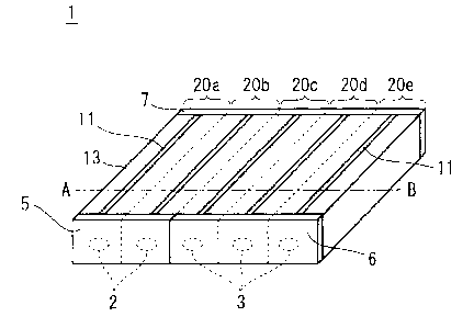
Fig. 1 is a perspective view of a semiconductor laser array 1 in this
preferred
embodiment. Fig. 2 is a cross-sectional view of the semiconductor laser array
1 in this
preferred embodiment (taken along an AB line of Fig. 1). As shown in Fig. 1,
the
semiconductor laser array 1 of the preferred embodiment includes a plurality
of laser
elements (namely, first to fifth laser elements 20a, 20b, 20c, 20d, 20e). The
first to fifth
laser elements are arranged in an array. Arranging them in the array refers to
the manner
that waveguides (not shown) in the adjacent laser elements are parallel to one
another.
The first laser element 20a includes a front-end-surface reflection film 5 on
a
front end surface serving as a light emitting surface of the waveguide.
Moreover, the
first laser element 20a includes a rear-end-surface reflection film 7 on a
rear end surface
opposite to the front end surface with the waveguide sandwiched between the
front end
surface and the rear end surface. A laser beam is emitted from a light
emitting point 2 of
the front-end-surface reflection film 5. In other words, the first laser
element 20a has a
structure of a unit resonator including the reflection films at both the ends
of the
waveguide. The second laser element 20b is also configured similarly.
The third laser element 20c includes a front-end-surface reflection film 6 on
a
front end surface serving as a light emitting surface of a waveguide (not
shown).
Moreover, the third laser element 20c includes the rear-end-surface reflection
film 7 on a
rear end surface opposite to the front end surface with the waveguide
sandwiched
between the front end surface and the rear end surface. A laser beam is
emitted from a
light emitting point 3 of the front-end-surface reflection film 6. In other
words, the third
CA 02875175 2014-12-15
7
laser element 20c has a structure of a unit resonator including the reflection
films at both
the ends of the waveguide. The fourth laser element 20d and the fifth laser
element 20e
are also configured similarly.
As shown in Fig. 1, the semiconductor laser array 1 has a structure in which
the
plurality of light emitting points 2 and 3 are aligned. The first to fifth
laser elements 20a,
20b, 20c, 20d, 20e do not have physical boundaries therebetween, so that Figs.
1 and 2
show the area corresponding to each of the laser elements separated by broken
lines for
the sake of convenience.
The front-end-surface reflection films 5, the front-end-surface reflection
films 6,
and the rear-end-surface reflection films 7 are dielectric multilayer films
for protecting
the end surfaces of the waveguides and controlling reflectances. The rear-end-
surface
reflection films 7 have the reflectance higher than that of the front-end-
surface reflection
films 5 and 6. The technology to make a reflectance of front-end-surface
reflection
films different from a reflectance of rear-end-surface reflection films in a
semiconductor
laser array for the purpose of high output operation of a light source is
generally known.
Furthermore, in the semiconductor laser array 1 of this preferred embodiment,
the front-end-surface reflection films 5 of the first and second laser
elements 20a, 20b and
the front-end-surface reflection films 6 of the third to fifth laser elements
20c, 20d, 20e
have different reflectances. In the preferred embodiment, if the value of the
reflectance
of the front-end-surface reflection films 5 is R5 and the value of the
reflectance of the
front-end-surface reflection films 6 is R6, the relationship R5 >R6 holds
true. R5 is, for
example, 30%, and R6 is, for example, 3%.
Fig. 3 is a diagram showing a reflectance distribution of the front-end-
surface
reflection films 5, 6 of the semiconductor laser array 1 in this preferred
embodiment. As
shown in Fig. 3, the front-end-surface reflection films 5 of the first and
second laser
CA 02875175 2014-12-15
8
elements 20a, 20b have the reflectance of 30% and the front-end-surface
reflection films
6 of the third to fifth laser elements 20c, 20d, 20e have the reflectance of
3%. The
reflectances of the front-end-surface reflection films 5 and 6 are set at such
values,
whereby the effect of the speckle noise reduction can be obtained.
As shown in Fig. 2, each laser element of the semiconductor laser array 1 is a
broad area laser. A lower cladding layer 8, an active layer 9, and an upper
cladding
layer 10 are laminated in the stated order on a substrate 14 (for example,
GaAs substrate).
A lower electrode 12 is provided on a lower surface of the substrate 14. Upper
electrodes 11 are provided on an upper surface of the upper cladding layer 10.
Insulating films 13 are formed between the upper electrodes 11.
The broad area laser generally has a simple structure as shown in Fig. 2, and
it
is characterized in that it enables high output in proportion to a width of
the upper
electrode 11. The insulating films 13 are made of Si02 or the like and
deposited for the
purpose of confining an injected current, preventing a leak current, and
protecting a
surface of the semiconductor.
<Manufacturing Method>
A method for manufacturing the semiconductor array 1 will be described.
First, the lower cladding layer 8, the active layer 9, and the upper cladding
layer 10 are
formed on the substrate 14 in which an initial growth occurs by a metal
organic chemical
vapor deposition method (MOCVD method) or the like. Next, waveguide patterns
corresponding to the waveguides of the first to fifth laser elements 20a, 20b,
20c, 20d, 20e
are formed by photolithography. The waveguide patterns are evenly spaced apart
from
one another. Moreover, the adjacent waveguide patterns are provided with a
distance
that does not cause mutual optical interference. Then, the insulating films 13
and the
upper electrodes 11 are formed. The method for manufacturing the general broad
area
CA 02875175 2014-12-15
9
laser includes these steps described above.
Next, a method for forming the front-end-surface reflection films 5 and the
front-end-surface reflection films 6 will be described. The
formation of the
front-end-surface reflection films 5, 6 includes a first vapor deposition step
and a second
vapor deposition step. First, in the first vapor deposition step, the front
end surfaces of
the first to fifth laser elements 20a, 20b, 20c, 20d, 20e are uniformly
irradiated with a
vapor deposition beam 16. The
irradiation continues until the time when the
front-end-surface reflection films 6 of the third to fifth laser elements 20c,
20d, 20e have
the thickness which can obtain the desirable reflectance (for example, 3%). As
a result,
a dielectric multilayer film (3% of reflectance) is uniformly formed on the
front end
surface of each laser element. Fig. 4A is a top view of the semiconductor
laser array 1
in the first vapor deposition step. In the first vapor deposition step, the
dielectric
multilayer film having the uniform thickness is formed, so that the front-end-
surface
reflection films 5 and the front-end-surface reflection films 6 have the same
thickness.
Next, the second vapor deposition step is performed. Fig. 4B is a top view of
the semiconductor laser array 1 in the second vapor deposition step. In the
second vapor
deposition step, the front-end-surface reflection films 6 of the third to
fifth laser elements
20c, 20d, 20e in a state of being covered with a shielding mask 15 are
irradiated with the
vapor deposition beam 16. The
irradiation continues until the time when the
front-end-surface reflection films 5 of the first and second laser elements
20a, 20b have
the thickness which can obtain the desirable reflectance (for example, 30%).
In the
second vapor deposition step, the shielding mask 15 partially blocks the vapor
deposition
beam 16, so that the dielectric multilayer film is not deposited on the front-
end-surface
reflection films 6.
As a result of the first and second vapor deposition steps, the reflectance
varies
CA 02875175 2014-12-15
between the front-end-surface reflection films 5 of the first and second laser
elements 20a,
20b (30% of reflectance) and the front-end-surface reflection films 6 of the
third to fifth
laser elements 20c, 20d, 20e (3% of reflectance).
A vapor deposition source which is a generation source of the vapor deposition
5 beam 16 is
omitted from Figs. 4A and 4B. Moreover, the rear end surface of each laser
element is irradiated with the vapor deposition beam until the time when its
thickness can
obtain the desirable reflectance (for example, 95%), and thus the dielectric
multilayer film
is uniformly deposited to form the rear-end-surface reflection films 7.
<Operation>
10 For the sake of
clear description, the first and second laser elements 20a, 20b
are a first group, and the third to fifth laser elements 20c, 20d, 20e are a
second group as
follows. In the
semiconductor laser array 1 of the preferred embodiment, the
front-end-surface reflection films 5 of the semiconductor elements of the
first group and
the front-end-surface reflection films 6 of the semiconductor elements of the
second
group have the different reflectances to emit light beams having different
wavelengths
from each of the front end surfaces. Moreover, the number of laser elements is
different
between the first group and the second group to uniformly output the light
beams having
the different wavelengths. The principle will be described below in detail.
As described above, the semiconductor laser array 1 has a structure in which
the
laser elements of the first group and the laser elements of the second group
are parallel to
one another. Thus, when each of the laser elements is driven under the same
condition,
a difference is generated in an oscillation threshold value between the laser
elements of
the first group and the laser elements of the second group. This can be seen
from a
threshold gain gth (unit [cm-1]) of the laser which is generally expressed by
the following
expression.
CA 02875175 2014-12-15
11
[Math 1 ] Fg,,, = a, + j-- log 1
2L Rf Rr
In the expression (1), F is an optical confinement factor of a waveguide, a,
is a
waveguide loss (unit [cm-1]), L is a resonator length of the waveguide (unit
[pm-1]), and
Rf and R, are reflectances of the front-end-surface reflection films 5, 6 of
the laser
elements and of the rear-end-surface reflection films 7 of the laser elements,
respectively.
The second term on the right side of the expression (1) corresponds to a
mirror loss an, of
the waveguide (unit [cm-1]). Here, in the semiconductor laser array 1, each
laser element
has the same waveguide structure, so that each laser element is equal in the
optical
confinement factor F as a parameter dependent on the waveguide structure, the
waveguide loss a1, and the resonator length L. Moreover, the rear-end-surface
reflection
film 7 of each laser element has the same reflectance Rr. In other words, only
the
reflectance Rf of the front-end-surface reflection films 5, 6 is different
between the laser
elements of the first group and the laser elements of the second group.
Therefore, the
threshold gain gth of the laser elements is a different value between the
first group and the
second group. The different threshold gain gth is equivalent to the different
oscillation
threshold value ith (unit [A]).
Here, considering that the reflectance R5 of the front-end-surface reflection
films 5 is higher than the reflectance R6 of the front-end-surface reflection
films 6 (R5>
R6), the expression (1) gives that the threshold gain gth of the laser
elements of the first
group is lower than the threshold gain gth of the laser elements of the second
group.
Therefore, the oscillation threshold value of the laser elements of the first
group (referred
to as 15) is lower than the oscillation threshold value of the laser elements
of the second
group (referred to as 16). Thus, the relationship 15<I6 holds true.
CA 02875175 2014-12-15
12
Here, without considering an influence of a change in the reflectance on an
output efficiency, the relationship between a current and an output of the
laser elements of
the first and second groups is shown in Fig. 5.
Note that each laser element (20a, 20b, 20c, 20d, 20e) of the semiconductor
laser array 1 is driven under the same condition. This can be easily achieved
by the
drive of a single power supply as long as the waveguide of each laser element
has the
same structure, namely, the same resistance. Therefore, if a drive current 10p
(unit [A]) is
given as a condition for driving each laser element, an output P5 (unit [W])
of the laser
elements of the first group becomes higher than an output P6 of the laser
elements of the
second group as shown in Fig. 5 (P5>P6).
A heating value AT (unit [K]) of the waveguide of each laser element in the
semiconductor laser array 1 is expressed by the following expression (2).
[Math 2] AT = (/(,1, = Vop ¨ P). Rth
Here, V01, (unit [V]) is a drive voltage, and Rth (unit [K/WI) is a heat
resistance
of the waveguide. Each laser element has the same drive condition (namely, LI,
and V0p)
and the same heat resistance Rth, so that only the output P on the right side
of the
expression (2) changes, the output P being dependent on the reflectances of
the
front-end-surface reflection films 5 and 6. Therefore, the laser elements of
the first
group and the laser elements of the second group have the different heating
value AT
corresponding to the output P. In other words, a heating value AT5 of the
laser elements
of the first group is lower than a heating value AT6 of the laser elements of
the second
group (AT5<AT6).
It is known that an oscillation wavelength of the laser element is shifted
according to the heating value AT of the waveguide. The degree of the shifted
CA 02875175 2014-12-15
13
wavelength is generally about 0.2 nm/K in red light and 0.05 nm/K in blue
light.
In other words, if a distribution is given to the reflectance of the
front-end-surface reflection films 5, 6 of each laser element forming the
semiconductor
laser array 1, a distribution occurs in the wavelength shift amount of the
output light
beams. This enables to output the laser beams having the different wavelengths
between
the laser elements of the first group and the laser elements of the second
group. The
wavelength shift amount Ak5 of the laser elements of the first group is
0.2xAT5 when the
laser beam is red. The wavelength shift amount AX 6 of the laser elements of
the second
group is 0.2><AT6 when the laser beam is red. Here, since the relationship
AT5<AT6
holds true as described above, the relationship Ak5<AX6 holds true.
The principle as described above makes the reflectance of the front-end-
surface
reflection films 5 of the semiconductor laser array 1 from that of the front-
end-surface
reflection films 6, which enables to multiplex the wavelengths of the output
light beams
of the semiconductor laser array 1. This can also reduce the speckle noise.
The amount of dispersion of the output P (namely, the amount of dispersion of
the heating value AT) between ones of laser element as shown in Fig. 6 is
actually
influenced by various factors. The main factor is an influence on the output
efficiency
due to the change in the reflectance.
First, an increase in the reflectance enhances the output efficiency because
of a
reduction in the waveguide loss. As described above, as the reflectance
increases, the
oscillation threshold value decreases. This reduces a free carrier density in
the
waveguide, which results in suppression of absorption of light.
On the other hand, the increase in the reflectance decreases the output
efficiency because of a reduction in the mirror loss. A loss of the laser
beams in the
mirror (namely, resonance end surface) is generally emitted as the output
light beams to
CA 02875175 2014-12-15
14
the outside of the resonator. Therefore, the high reflectance means that the
light is
hardly emitted to the outside. This is equivalent to the reduction in the
output efficiency.
As described above, the output efficiency changes according to the reflectance
of the front-end-surface reflection films 5, 6, and thus it is actually
difficult to make the
outputs from the laser elements of the first and second groups in parallel to
each other as
shown in Fig. 5. However, the appropriate setting of the drive current lop can
distribute
the outputs of the laser elements of the first and second groups, and thus the
difference in
the heating value of the waveguides between the laser elements of the first
and second
groups can be adjusted.
Fig. 6 is a diagram showing a reflectance dependence of the front-end-surface
reflection films 5, 6 on the output P and the wavelength shift amount 4X of
the laser
elements. The horizontal axis of Fig. 6 shows the reflectance Rf of the front-
end-surface
reflection films 5, 6. The vertical axes of Fig. 6 each show the wavelength
shift amount
A. and the output P. In Fig. 6, the rear-end-surface reflection films 7
constantly have
the reflectance R, of 95%. Fig. 6 is an example showing the influence of the
change in
the reflectance Rf of the front end surfaces on the wavelength shift amount AX
and the
output P.
It can be seen from Fig. 6 that when the front-end-surface reflection films 5
of
the laser elements of the first group have the reflectance (R5) of 30% and the
front-end-surface reflection films 6 of the laser elements of the second group
have the
reflectance (R6) of 3%, the difference in the wavelength shift amount AX is
approximately
2 nm. The output light beams of the semiconductor laser array 1 have the
spectral width
of 2 nm, which can place expectations on the sufficient effect of the speckle
noise
reduction.
On the other hand, as shown in Fig. 6, the output of the laser elements
greatly
CA 02875175 2014-12-15
fluctuates with the change in the reflectance of the front-end-surface
reflection films 5, 6.
As shown in Fig. 6, as the reflectance Rf increases, the output P increases.
As with the preferred embodiment, in a case of multiplexing the wavelengths of
the semiconductor laser array 1 to reduce the speckle noise, the output values
of the light
5 beams having
the different wavelengths are preferably close to each other. Thus, in the
semiconductor laser array 1 of the preferred embodiment, the laser elements of
the first
group are fewer than the laser elements of the second group.
In other words, in the preferred embodiment, the first and second laser
elements
20a, 20b including the front-end-surface reflection films 5 having the
relatively high
10 reflectance
(namely, laser elements producing high output) are fewer than the third to
fifth laser elements 20c, 20d, 20e including the front-end-surface reflection
films 6 having
the relatively low reflectance (namely, laser elements producing low output).
This
enables to bring the two outputs of the output light beams having the
different
wavelengths close to each other.
15 In the
semiconductor laser array 1 shown in Fig. 1 of the preferred embodiment,
the two laser elements (first and second laser elements 20a, 20b) include the
front-end-surface reflection films 5 having the relatively high reflectance
(for example,
30%) and the three laser elements (third to fifth laser elements 20c, 20d,
20e) include the
front-end-surface reflection films 6 having the relatively low reflectance
(for example,
3%), to thereby uniformalize the outputs between the output light beams having
the
different wavelengths.
<Effects>
The semiconductor laser array 1 of the preferred embodiment including the
plurality of laser elements (namely, first to fifth laser elements 20a, 20b,
20c, 20d, 20e) is
characterized as follows. The plurality of laser elements are disposed such
that the
CA 02875175 2014-12-15
16
waveguides of the laser elements are parallel to one another. Each of the
plurality of
laser elements includes the front-end-surface reflection film 5, 6 on the
front end surface
serving as the light emitting surface of the waveguide. Each of the plurality
of laser
elements includes the rear-end-surface reflection film 7 on the rear end
surface opposite
to the front end surface with the waveguide sandwiched between the front end
surface and
the rear end surface. The front-end-surface reflection films 5, 6 of at least
two of the
plurality of laser elements have different reflectances. The rear-end-surface
reflection
films 7 of the plurality of laser elements have the same reflectance. The
plurality of
laser elements are driven by a single power supply.
Therefore, the semiconductor laser array 1 of the preferred embodiment has the
simple structure in which the front end surface reflectance films 5 and 6 of
the plurality of
laser elements have the different reflectances, which allows for the speckle
noise
reduction by multiplexing the wavelengths of the semiconductor laser array I.
The
reflectance of the front-end-surface reflection films 5, 6 can be easily
adjusted with
accuracy, so that the semiconductor laser array 1 can be easily obtained.
The technique to multiplex the wavelengths of the semiconductor laser array 1
by changing the reflectance of the front-end-surface reflection films can be
applied to the
broad area laser having one of the simplest structures as the laser element.
In other
words, the broad area laser is adopted as the structure of the laser element,
which enables
to multiplex the wavelengths of the semiconductor laser array easily.
Furthermore, the semiconductor laser array 1 of the preferred embodiment can
multiplex the wavelengths by making the reflectance of the front-end-surface
reflection
films 5, 6 of the plurality of laser elements having the same structure
different from each
other, and this eliminates the need to change the internal structure of the
semiconductor
laser array for multiplexing the wavelengths. In other words, the process
of
CA 02875175 2014-12-15
17
manufacturing the semiconductor laser array 1 does not need to carry out a
plurality of
crystal growth unlike Japanese Patent Application Laid-Open No. 2000-11417.
Moreover, space between the waveguides does not require modulation unlike
Japanese
Patent Application Laid-Open No. 2008-4743, so that the semiconductor laser
array 1 of
the preferred embodiment is excellent in productivity.
The unnecessity of carrying out the plurality of crystal growth of the
semiconductor in the manufacturing process is advantageous for reliability. In
other
words, the semiconductor laser array 1 of the preferred embodiment includes
the active
layer made of good-quality semiconductor crystals having less lattice defects,
which
allows the laser array 1 to drive high output for a long time.
In the semiconductor laser array 1 of the preferred embodiment, the plurality
of
laser elements have the same structure, and the waveguides of the laser
elements are
evenly spaced apart from one another. The waveguide of each laser element is
disposed
with a sufficient distance that does not cause mutual optical interference.
Therefore, the
semiconductor laser array 1 of the preferred embodiment can prevent an
unstable
operation which is a problem in the technique to modulate the space between
the
waveguides to multiplex the wavelengths and is caused by the optical
interference
between the adjacent laser elements.
The semiconductor laser array 1 of the preferred embodiment can set many
conditions only with the adjustment to the reflectance of the front-end-
surface reflection
films 5 and the front-end-surface reflection films 6, so that the
semiconductor laser array
1 can be compatible with various required specifications.
In the semiconductor laser array 1 of the preferred embodiment, the waveguide
of each laser element has the same structure, so that each laser element can
be driven
under the same condition by connecting each electrode to the same power
supply. In
CA 02875175 2014-12-15
18
other words, a complicated drive circuit is not needed, and thus it is
advantageous for the
mechanism and the cost. Here, the semiconductor laser array 1 can be driven by
the
single power supply because the waveguide of each laser element has the same
structure
and the semiconductor laser array 1 can be driven as the "parallel circuit in
which the
waveguide of each laser element has the same resistance."
In the semiconductor laser array 1 of the preferred embodiment, the plurality
of
laser elements having the different oscillation wavelengths can be
simultaneously driven
by the single power supply, so that the semiconductor laser array 1 is also
preferably
applicable as the light source of the display device. The reason is that the
screen is
needed to be irradiated with the light beams having the wide spectral width,
namely, the
light beams multiplexing the wavelengths in order to achieve the speckle noise
reduction.
Each laser element of the semiconductor laser array 1 can be configured to be
not only a gain-guiding type (for example, broad area laser) having a simple
structure but
also to be a refractive index-guiding type (for example, ridge type laser and
buried hetero
laser). In both cases, a plurality of laser elements having the same structure
are formed
on the same substrate, and thus the plurality of laser elements can be easily
driven under
the same condition, whereby the effects of the present invention can be fully
exhibited.
In the semiconductor laser array 1 of the preferred embodiment, the plurality
of
laser elements (namely, first to fifth laser elements 20a, 20b, 20c, 20d, 20e)
include the
first group and the second group, the front-end-surface reflection films 5 of
the laser
elements (first and second laser elements 20a, 20b) forming the first group
have the first
reflectance (namely, reflectance R5), the front-end-surface reflection films
of the laser
elements (third to fifth laser elements 20c, 20d, 20e) forming the second
group have the
second reflectance (namely, reflectance R6), and the first reflectance is
higher than the
second reflectance. In a case where an output of the laser elements increases
as the
CA 02875175 2014-12-15
19
reflectance of the front-end-surface reflection films 5, 6 increases, the
laser elements
1
forming the first group are fewer than the laser elements forming the second
group. In a
case where an output of the laser elements decreases as the reflectance of the
front-end-surface reflection films 5, 6 increases, the laser elements forming
the first group
5 are more than the laser elements forming the second group.
In the preferred embodiment, the front-end-surface reflection films 5 of the
laser elements of the first group has the reflectance R5 higher than the
reflectance R6 of
the front-end-surface reflection films 6 of the laser elements of the second
group (R5>R6).
As shown in Fig. 6, the output of the laser elements in the preferred
embodiment
10 increases
as the reflectance of the front-end-surface reflection films increases.
Therefore,
the laser elements (first and second laser elements 20a, 20b) of the first
group producing
the relatively high output are fewer than the laser elements (third to fifth
laser elements
20c, 20d, 20e) of the second group producing the relatively low output. This
can reduce
the difference in the output between the groups.
15 In the
semiconductor laser array 1 of the preferred embodiment, the plurality of
laser elements (namely, first to fifth laser elements 20a, 20b, 20c, 20d, 20e)
are formed on
the same substrate, and the plurality of laser elements have the same
characteristics
except for the reflectance of the front-end-surface reflection films 5 and 6.
Therefore, after the plurality of laser elements (namely, first to fifth laser
20 elements
20a, 20b, 20c, 20d, 20e) are formed on the same substrate to manufacture the
laser array by the manufacturing method similar to the method for
manufacturing the
general laser array, the front-end-surface reflection films 5 and the front-
end-surface
reflection films 6 only have the different reflectances, whereby the
semiconductor laser
array 1 can easily be obtained.
25 In the
semiconductor laser array 1 of the preferred embodiment, the plurality of
CA 02875175 2014-12-15
laser elements (first to fifth laser elements) are broad area lasers.
Therefore, the laser elements are the broad area lasers which are easily
manufactured, and thus the semiconductor laser array 1 can easily be obtained.
<Second Preferred Embodiment>
5 Fig. 7 is a
diagram showing a reflectance distribution of front-end-surface
reflection films of a semiconductor laser array according to this preferred
embodiment.
In the first preferred embodiment (Fig. 3), the plurality of laser elements
are disposed in
order of the first, second, third, fourth, and fifth laser elements. On the
other hand, in
the preferred embodiment, as shown in Fig. 7, a plurality of laser elements
are disposed in
10 order of third,
first, fourth, second, and fifth laser elements. In other words, the laser
elements including the front-end-surface reflection films of the different
reflectances are
disposed alternately. The configuration except for this is the same as the
configuration
in the first preferred embodiment, and thus the description will be omitted.
<Effect>
15 In the
semiconductor laser array 1 of the preferred embodiment, the laser
elements including the front-end-surface reflection films of the different
reflectances are
disposed alternately.
Therefore, the laser elements including the front-end-surface reflection films
of
the different reflectances are disposed alternately, which enables to
uniformalize the
20 spatial
distribution of the wavelength of the output light beam of the semiconductor
laser
array I.
<Third Preferred Embodiment>
Fig. 8 is a diagram showing a reflectance distribution of front-end-surface
reflection films of a semiconductor laser array according to this preferred
embodiment.
In the preferred embodiment, the semiconductor laser array includes first to
sixth laser
CA 02875175 2014-12-15
21
elements. The first to sixth laser elements are disposed such that waveguides
of the laser
elements are parallel to one another similarly to the first preferred
embodiment.
In this preferred embodiment, a front-end-surface reflection film of a first
laser
element has a reflectance RI. Front-end-surface reflection films of a second
and a third
laser elements have a reflectance R2. Front-end-surface reflection films of a
fourth to
sixth laser elements have a reflectance R3. Here, the relationship RI>R2>R3
holds true.
The configuration except for this is the same as the configuration in the
first preferred
embodiment, and thus the description will be omitted.
In this manner, the plurality of laser elements have the three types of the
reflectances of the front-end-surface reflection films, whereby the
wavelengths of the
semiconductor laser array can be multiplexed by superimposing the three
different
wavelengths. Thus, the spectral width of the output light beams can be
expanded more
than that in the first preferred embodiment, allowing for further improvements
in the
effects of reducing the speckle noise.
In addition, according to the present invention, the above preferred
embodiments can be arbitrarily combined, or each preferred embodiment can be
appropriately varied or omitted within the scope of the invention.
While the invention has been shown and described in detail, the foregoing
description is in all aspects illustrative and not restrictive. It is
therefore understood that
numerous modifications and variations can be devised without departing from
the scope
of the invention.