Note: Descriptions are shown in the official language in which they were submitted.
CA 02875262 2014-12-01
WO 2013/177678 PCT/CA2013/000524
METHOD AND SYSTEM FOR MAGNETIC SEMICONDUCTOR SOLID STATE
COOLING
CROSS-REFERENCE TO RELATED APPLICATIONS
[001] This patent application claims the benefit of U.S. Provisional Patent
Application US
61/652,931 filed May 30, 2012 entitled "Method and System for Magnetic
Semiconductor Solid
State Cooling", the entire contents of which are included by reference.
FIELD OF THE INVENTION
[002] The present invention relates to magnetic cooling and more
specifically magnetic
cooling in semiconductor substrates and devices.
BACKGROUND OF THE INVENTION
[003] In physics, cryogenics is the study of the production of very low
temperatures (below
¨150 C, ¨238 F or 123K) and the behavior of materials at those temperatures.
Cryogenic
electronics, the operation of electronic devices, circuits, and systems at
cryogenic temperatures,
has been a valuable technology for decades. Cryogenic electronics can be based
on
semiconductive devices, on superconductive devices, or on a combination of the
two. The
investigation and application of semiconductor devices, e.g. diodes and
transistors, at low
temperatures was underway during the 1960s-1970s and has continued such that
semiconductor
electronics has since expanded into many areas, based on integrated circuits
as well as
transistors.
[004] Such semiconductor-based cryogenic electronics can be as simple as a
circuit using a
single transistor (or diode) or as complex as a system incorporating hundreds
of large integrated
circuits. It includes both analog and digital systems, spans the frequency
spectrum from DC to
100s of GHz, and ranges in power from microwatts to hundreds of watts.
Transistors types
include both bipolar and field-effect, using Si, Ge, GaAs, SiGe and III-V
semiconductor
materials. Cryogenic electronic circuits are used not only in the laboratory,
but hundreds have
been used "in the field" in practical applications, and several types are
available commercially.
- 1 -
CA 02875262 2014-12-01
WO 2013/177678 PCT/CA2013/000524
There are two broad reasons for operating electronics at cryogenic
temperatures, first being to
improve the performance of the electronics (lower noise, higher speed,
increased efficiency,
etc.), and second because electronics are required to support a sensor,
actuator or other apparatus
residing in a cryogenic environment. Some applications may combine both
reasons. Related
benefits of cryogenic operation may include improved thermal and electrical
conductivity, lower
operating power, reduction of parasitic losses, diminished chemical and
metallurgical
degradation, and improved overall reliability.
[005] Historically cryogenic electronics have exploited liquid inert
refrigerants such as
nitrogen (II) oxide (121K), argon (87K), liquid nitrogen (77K), neon (27K),
and helium (4K) to
provide the required ambient temperature of operation. In some instances
thermoelectric coolers,
typically Peltier devices, are employed in conjunction with particular
refrigerants, such as liquid
nitrogen, to obtain intermediate temperatures. However, in all such instances
the electronic
circuit must be sealed within a housing thermally isolating the electronics
from ambient
increasing the size, weight and cost of cryogenic electronics. Accordingly it
would be beneficial
to provide a means of providing cryogenic cooling of electronics with reduced
complexity,
reduced ancillary hardware requirements, and cost. In other instances it may
be beneficial to
provide cryogenic cooling to part of an electronic circuit without cooling the
entire circuit.
[006] Magnetic refrigeration is a cooling technology based on the
magnetocaloric effect
which has been used to attain extremely low temperatures, as well as provide
cooling over
temperature ranges used in common refrigerators, depending on the design of
the system. The
effect was first observed by Emil Warburg (1880) and the fundamental principle
was suggested
by Debye (1926) and Giauque (1927) with the first working magnetic
refrigerators were
constructed by several groups beginning in 1933 and was the first method
developed for cooling
below approximately 0.3 K which is attainable using 3He refrigeration. Using
magnetic
refrigeration temperatures in the micro-Kelvin ( ) to milli-Kelvin ( mK )
ranges.
[007] The mechanism involves a material in which some aspect of disorder of
its constituent
particles exists at low temperature, for example at liquid helium temperatures
of 4K (4 He) or
0.3K (3.11e). Magnetic dipoles in a crystal of paramagnetic salt, e.g.
gadolinium sulfate
Gd2(SO4)3 = (H20)8 or cerium magnesium nitrate Ce2Mg3(NO3)12 = (1120)24 , have
this property
- 2 -
CA 02875262 2014-12-01
WO 2013/177678 PCT/CA2013/000524
of disorder in that the spacing of the energy levels of the magnetic dipoles
is small compared
with the thermal energy. For paramagnetic salts the active magnetic dipoles
are those of the
electron shells of the paramagnetic atoms. Under these conditions the dipoles
occupy these levels
equally, corresponding to being randomly oriented in space. When a magnetic
field is applied,
these levels become separated sharply; i.e., the corresponding energies are
widely different, with
the lowest levels occupied by dipoles most closely aligned with the applied
field. If the magnetic
field is applied while the paramagnetic salt is in contact with the liquid
helium heatsink, an
isothermal process in which a constant temperature is maintained, many more
dipoles will
become aligned, with a resultant transfer of thermal energy to the heatsink.
[008] If the magnetic field is decreased after contact with the heatsink
has been removed, no
heat can flow back in (an adiabatic process), and the paramagnetic salt sample
will cool. Such
cooling corresponds to the dipoles remaining trapped in the lower energy
states, i.e. aligned.
Temperatures from 0.3K to as low as 0.0015K have been demonstrated through
such
paramagnetic salt samples. Much lower temperatures can be attained by an
analogous means
called adiabatic nuclear demagnetization which relies on ordering (aligning)
nuclear dipoles
(arising from nuclear spins), which are at least 1,000 times smaller than
those of atoms. With this
process, temperatures of the ordered nuclei as low as 16 fiK (0.000016K)
absolute have been
demonstrated.
[009] In both techniques, spins are polarized at an initial high magnetic
field B, at an initial
temperature T1, and the magnetic field is then adiabatically swept to a low
final field B1. Owing
to the adiabatic nature of the magnetic field sweep, the initial spin
temperature T, is reduced to a
final spin temperature T1 = T, x (13 f 13,). The electron and phonon degrees
of freedom at T, are
subsequently cooled by heat exchange with spins at the lower temperature Tf.
[0010] Accordingly such solid state refrigeration may be employed to cool
an electronic
circuit to provide a cryogenic electronic circuit although the same
constraints as described supra
in respect of cooling the whole electronic circuit remain. Additionally, it is
necessary to provide
paramagnetic salts in substrate form allowing the electronic circuit,
typically formed upon a
silicon substrate, to be mounted upon it. It would be beneficial therefore to
remove the
- 3 -
CA 02875262 2014-12-01
WO 2013/177678 PCT/CA2013/000524
requirement for such materials by providing direct magnetic cooling of the
electronic circuit
substrate or a predetermined portion of the electronic circuit and / or
electronic circuit substrate.
In general form it would be beneficial to be able to provide direct magnetic
cooling of
semiconductor materials including but not limited to Si, Ge, GaAs, SiGe, InP,
AlGaAs,
InGaAsP.
[0011] According to embodiments of the invention direct cooling of a
semiconductor, e.g.
silicon, is achieved through demagnetization of electron spins bound to donor
impurity atoms.
The entropy of donor-bound electron spins in heavily doped silicon, for
example, dominates over
both phonon entropy and electron gas entropy at low temperatures and moderate
magnetic fields,
see for example Lakner et al in "Localized Magnetic Moments in Si:P near the
Metal-Insulator
Transition" (Phys. Rev. B, Vol. 50, pp17064-17073) and Wagner et al in
"Specific Heat of
Si:(P,B) at Low Temperatures" (Phys. Rev. B 55, 4219-4224), thus enabling
effective cooling by
demagnetization. Direct magnetic cooling of silicon substrates as outlined
above being of
practical importance for silicon device applications in cryogenic electronics
requiring low
temperatures, including, but not limited to silicon based quantum computing,
see for example
Maune et al in "Coherent Singlet-Triplet Oscillations in a Silicon-Based
Double Quantum Dot"
(Nature, Vol. 481, pp344-347), and transition edge single photon detectors,
see for example Lita
et al in "Counting Near-Infrared Single-Photons with 95% Efficiency" (Opt.
Exp., Vol. 16,
pp3032-3040).
[0012] Beneficially active electronic devices can be integrated
monolithically atop a
semiconductor substrate exhibiting magnetic refrigeration within the whole
substrate or
predetermined regions of the substrate. Alternatively, active electronic
devices may be formed
with semiconductor layers integral within them that exhibit magnetic cooling.
[0013] Other aspects and features of the present invention will become
apparent to those
ordinarily skilled in the art upon review of the following description of
specific embodiments of
the invention in conjunction with the accompanying figures.
- 4 -
CA 02875262 2014-12-01
WO 2013/177678 PCT/CA2013/000524
SUMMARY OF THE INVENTION
[0014] It is an object of the present invention to enable magnetic cooling
and more
specifically magnetic cooling in semiconductor substrates and devices.
[0015] In accordance with an embodiment of the invention there is provided a
method
comprising:
(a) providing a device comprising at least a semiconductor material comprising
spins at a
predetermined density within a magnetic field;
(b) cycling the magnetic field from a first predetermined value to a second
predetermined value
at a first predetermined rate to establish a first condition for a
predetermined portion of
the spins;
(c) extracting thermal energy generated within the semiconductor material
through step (b);
(d) increasing the thermal isolation of the semiconductor material to its
surroundings; and
(e) cycling the magnetic field from a third predetermined value to a fourth
predetermined value
at a second predetermined rate to establish a second condition for a
predetermined
portion of the spins.
[0016] In accordance with an embodiment of the invention there is provided
a device
comprising:
a substrate comprising a first semiconductor material;
an element comprising a second semiconductor material comprising spins at a
predetermined
density;
an electrically adjustable thermal barrier formed within the substrate between
the element and
the substrate, wherein
the second semiconductor material may be cooled in dependence upon executing a
predetermined sequence of steps relating to the electrically adjustable
thermal barrier and
a variable magnetic field within which the device is located.
[0017] In accordance with an embodiment of the invention there is provided
a method
comprising:
providing a semiconductor heterostructure comprising a spatially varying Lande
g-factor from a
first predetermined value to a second predetermined value;
- 5 -
CA 02875262 2014-12-01
WO 2013/177678 PCT/CA2013/000524
applying a predetermined magnetic field to the semiconductor heterostructure;
biasing the semiconductor heterostructure at a voltage that is less than the
thermal voltage of the
semiconductor heterostructure; wherein
a resulting current flow within the semiconductor heterostructure results in
continuous cooling of
the side of the semiconductor heterostructure with the Lan& g-factor with the
first
predetermined value.
[0018] In accordance with an embodiment of the invention there is provided
a device
comprising:
a semiconductor heterostructure comprising a spatially varying Lande g-factor
from a first
predetermined value to a second predetermined value;
a circuit applying a bias to the semiconductor heterostructure at a voltage
that is less than the
thermal voltage of the semiconductor heterostructure; wherein
a resulting current flow within the semiconductor heterostructure when a
predetermined
magnetic field is applied results in continuous cooling of the side of the
semiconductor
heterostructure with the Lande g-factor with the first predetermined value.
[0019] Other aspects and features of the present invention will become
apparent to those
ordinarily skilled in the art upon review of the following description of
specific embodiments of
the invention in conjunction with the accompanying figures.
BRIEF DESCRIPTION OF THE DRAWINGS
[0020] Embodiments of the present invention will now be described, by way of
example only,
with reference to the attached Figures, wherein:
[0021] Figures lA and 1B depict reduced entropy and magnetization per spin
as a function of
temperature and magnetic field;
[0022] Figures 2A and 2B depict spin entropy and specific versus for
different magnetic fields
as a function of temperature;
[0023] Figure 3 depicts the adiabatic heat transfer for a Si:As sample
according to an
embodiment of the invention;
- 6 -
CA 02875262 2014-12-01
WO 2013/177678 PCT/CA2013/000524
[0024] Figure 4 depicts specific isothermal cooling for a for a Si:As
sample according to an
embodiment of the invention with varying temperature and magnetic field;
[0025] Figure 5 depicts the maximum isothermal cooling for a Si:As sample
according to an
embodiment of the invention;
[0026] Figure 6 depicts a Si:As sample with graphene 4-point thermometer
according to an
embodiment of the invention;
[0027] Figure 7 depicts the resistance versus temperature and magnetic
field measured for the
graphene thermometer on the Si:As sample according to an embodiment of the
invention;
[0028] Figure 8A depicts the measured resistance of the graphene
thermometer on the Si:As
sample according to an embodiment of the invention at different magnetic field
sweep rates;
[0029] Figure 8B depicts the derived temperature change of the Si:As sample
according to an
embodiment of the invention under magnetic field sweeping at different initial
temperatures;
[0030] Figure 9A depicts a simple model for cooling of a semiconductor
material according to
an embodiment of the invention;
[0031] Figure 9B depicts simulation results for a Si:As sample using the
simple model of
Figure 9A;
[0032] Figure 10 depicts transition edge sensors which may be implemented
onto solid state
coolers exploiting semiconductor materials according to embodiments of the
invention;
[0033] Figure 11 depicts an AC Josephson superconducting junction which
forms part of
hybrid normal-conducting device with an unbiased InAs nanowire integrable with
solid state
cooling methodologies according to embodiments of the invention;
[0034] Figure 12 depicts a Josephson Junction based quantum-bit memory and
metallization
interconnect integrable with solid state cooling methodologies according to
embodiments of the
invention;
[0035] Figure 13 depicts a 2nd order bandpass sigma-delta analog-to-digital
converter
exploiting superconducting Josephson Junctions and integrable with solid state
cooling
methodologies according to embodiments of the invention;
[0036] Figure 14 depicts a self-assembled SiGe nanocrystal within a
junction supporting two-
dimensional Qu-bit architectures integrable with solid state cooling
methodologies according to
embodiments of the invention;
- 7 -
CA 02875262 2014-12-01
WO 2013/177678 PCT/CA2013/000524
[0037] Figure 15 depicts a dot-within-a-dot-in-a-nanowire structure
integrable with solid state
cooling methodologies according to embodiments of the invention;
[0038] Figure 16 depicts a nanotube manufacturing methodology and exemplary
layer
structures nanotubes integrable with solid state cooling methodologies
according to embodiments
of the invention;
[0039] Figure 17 schematics of photoelectrochemical device and
electrobiological device
respectively according to embodiments of the invention exploiting dot-in-a-
wire structures
[0040] Figure 18 depicts stacked solid state cooler configurations
according to embodiments
of the invention;
[0041] Figure 19A depicts an exemplary process flow for a solid state
cooling cycle according
to an embodiment of the invention;
[0042] Figures 19B and 19C depict exemplary electrical structures for
thermally isolating a
solid state cooler according to embodiments of the invention allowing a
cooling cycle such as
depicted in Figure 19A to be implemented with electrical control of the solid
state cooler and
magnetic field; and
[0043] Figure 20 depicts a schematic of the Zeeman energy in a
heterostructure along the
growth direction for continuous solid state cooling according to an embodiment
of the invention.
DETAILED DESCRIPTION
[0044] The present invention is directed to magnetic cooling and more
specifically magnetic
cooling in semiconductor substrates and devices.
[0045] The ensuing description provides exemplary embodiment(s) only, and
is not intended
to limit the scope, applicability or configuration of the disclosure. Rather,
the ensuing description
of the exemplary embodiment(s) will provide those skilled in the art with an
enabling description
for implementing an exemplary embodiment. It being understood that various
changes may be
made in the function and arrangement of elements without departing from the
spirit and scope as
set forth in the appended claims.
[0046] 1: THEORY: DONOR BOUND SPIN MODEL FOR COOLING
SEMICONDUCTORS
- 8 -
CA 02875262 2014-12-01
WO 2013/177678 PCT/CA2013/000524
[0047] Within this section two simple models for cooling/heating via the
localized spins on
donor bound electrons in a semiconductor, e.g. silicon (Si) are summarised.
Whilst the
discussions refer to silicon it would be evident that the basic principles
apply for donor bound
electrons in other semiconductors. The first model is adiabatic
demagnetization, where the spins
are cooled adiabatically, after which the surrounding matter equilibrates with
the spins and an
absolute bound on the heat transfer Q is imposed by this model. The second
model is isothermal
demagnetization, where the spin time constant T, is so short that spins
equilibrate with
surrounding matter almost instantaneously during demagnetization. An absolute
bound on the
rate of heat transfer Q is imposed by this model. Physical embodiments
according to
embodiments of the invention typically lie somewhere in between these two
models.
[0048] Within the prior art numerous experiments have been reported on the
properties of
donor bound electrons (mostly P-doped Si and to a lesser extent As-doped Si),
including electron
spin resonance, magnetic susceptibility and specific heat measurements.
Surprisingly, at doping
densities above the metal-insulator transition (MIT), where there is an
electron gas present in the
Si at low temperatures (4.2K and below), signatures of localized magnetic
moments are still
observed in magnetic susceptibility and specific heat. According to
experimental embodiments
of the invention the inventors have employed As-doped Si (also referred to as
Si:As) samples
having an As doping density estimated to be 1020 /cc based on room temperature
sheet
resistance, which is above the MIT critical density since conduction persists
at T = 4.2K. It is
noted that at this point in time there is no complete theory for the magnetic
properties of donor
bound electrons in the presence of an electron gas.
[0049] The critical energy scale for antiferromagnetic ordering in the
presence of dipole
interactions alone determines a lower bound for the temperature and magnetic
field at which the
spins of donor bound electrons can be considered independent. At 1020 / cc,
the average dopant
spacing is r = 2.15nm , which corresponds to a dipole-dipole interaction given
by Equation (1)
below of V = 5neV or T. = 631uK . As such we expect electron spin ordering at
ultralow
temperatures, although the effect of exchange interactions mediated by free-
electrons is expected
to increase the critical temperature for spin ordering.
- 9 -
CA 02875262 2014-12-01
WO 2013/177678 PCT/CA2013/000524
V Po B (1)
(47zr3)
[0050] 1A: Fundamental Properties: The thermodynamic properties of
localized electrons
with paramagnetic response are well known within the prior art, see for
example Pathria in "
Statistical Mechanics" (Pergamon Press, ISBN 978-0123821881) and Pobell in
"Matter and
Methods at Low Temperatures" (Springer Verlag, ISBN 978-3540463566). For N
donor bound
electron spins with Zeeman energies c= gpBB = - ,uBB , corresponding to a
Lamle g-factor of
g= 2 appropriate for a conduction electron in Si, the free-energy A, entropy
S, total energy
U, magnetization M and heat capacity C are given by Equations (2) to (6)
respectively below.
p \
A=¨NkBT1n 2 coshB
B (2)
\kBT }
6.A` /11 r
S = = Nk13 In 2 cosh5B \} pBB tanh _______________________________ (3)
kB T kB T kB T
y3T
r p,B\
U = A+TS =¨NpBBtanh T (4)
k
\
cSA\ ( B\
M ___________________ =Np ,u,
Btanh _____________________________ (5)
k T
B
C =I -(5u \ = NkitiBB\ sec h (
2 11 BB
(6)
k T k T
[0051] The reduced entropy per spin, S/NkB , tends to ln 2 = 0.693 at
temperatures high
compared to Zeeman energy in an applied magnetic field, i.e. kBT > pBB , as
shown in Figure
1A for different temperatures. The reduced magnetization per spin, MIN B,
plotted in Figure
1B for different temperatures, shows the onset of complete spin polarization
with applied field at
low temperatures.
[0052] 1B: Entropy and Heat Capacity: For the purpose of heat exchange, the
specific
entropy S per cc of Si:As and the specific heat capacity C C per cc of Si:As
for a given donor-
bound electron density c. Both quantities are in direct proportion to the
density of localized
magnetic moments of donor-bound electrons, and are plotted in Figures 2A and
2B respectively
- 10-
CA 02875262 2014-12-01
WO 2013/177678 PCT/CA2013/000524
for varying temperature. It has been assumed that 10% of the electrons are
bound to the 1020 / cc
As dopants. For comparison the total heat capacity of Si:P at 1K was measured
by the inventors
as cz-, ¨ 5 pf 1 ccK . Accordingly for 10% donor bound electrons, i.e. 1019
/cc spin density, a
0.05cc Si sample provides a peak entropy of 4.8pJ/ K and a peak heat capacity
of 3.01uf/ K . It
is evident from Figures 2A and 2B the peak specific entropy and the peak
specific heat are
independent of temperature and magnetic field for fixed number of spins.
Rather it is the total
number of spins that determines the peak entropy and heat capacity of the
system overall. The
peak heat capacity Cpeak of a sample with N donor bound electrons occurs at a
temperature
Tpõk is given by Equations (7A) and (78) below.
C peak = 0.439 = Nk (7A)
itiBB = 1.20 = kB Tpõk (7B)
100531 1C: Adiabatic Demagnetization and Heat Flow: Adiabatic demagnetization
of spins
proceeds by ramping a magnetic field from an initial B, to a final Bf while
maintaining
constant entropy in the spins. This requires the normalized sweep rate BIB to
be fast compared
to the spin relaxation rate 1/11 , but slow compared to resonant frequency co
= guBB I h. In this
classic form of refrigeration by adiabatic demagnetization, the spins are
first made cold, after
which the lattice equilibrates with the spins. Under adiabatic sweep
conditions, the initial spin
temperature T, and final spin temperature T1 are governed by T1 IT =B 11B, .
The heat Q that
can be absorbed by highly polarized (low entropy) spins cooled to a final
temperature T1 at the
final magnetic field B1 is given by Equation (8) below.
jsy
Q= T ____ dT = CdT (8)
D I
where Equation (9) follows from the relation between entropy and heat
capacity,
( SS C
¨ (9)
T B T
-11-
CA 02875262 2014-12-01
WO 2013/177678
PCT/CA2013/000524
[0054]
Assuming that the final spin temperature Tf is much less than the temperature
T,õõ of
peak heat capacity, the total heat that can be absorbed by the spins is the
area under the C versus
T curve given by Equation (10) below. In other words, the maximum heat that
can be absorbed
by N fully polarized spins is the energy required to flip 50% of the spins at
a cost of guBB
1.
Q = f CdT = N,uBB
(10)
[0055]
Whether the demagnetization process is adiabatic or not, it is clear that
gAIBBr is the
absolute maximum heat that can be transferred into the spins. The final
magnetic field Bf
determines the final spin temperature as Tr =-T,=Br.
and the Si cannot be made any colder.
The final magnetic field B also sets the total heat Q that can be absorbed,
wherefore it is
advantageous to use a larger Br to increase the heat that can be absorbed at
the expense of a
higher final temperature. The maximum heat that can be absorbed by donor bound
electrons in a
0.05cc Si:As sample at a final field of Br =100mT is depicted in Figure 3.
[0056] 1D: Demagnetization with Fast Spin-Lattice Relaxation: Non-Adiabatic
Demagnetization: Adiabatic demagnetization requires no change in spin entropy,
and hence no
change in spin polarization, during the sweeping of the magnetic field.
However, as noted below
in respect of experimental results for a Si:As sample with a graphene based
four-point resistance
probe a significant graphene resistance, and hence temperature, change during
the sweep was
observed.
[0057]
The donor bound electron spin longitudinal relaxation time Ti has been studied
extensively in Si:P. While most recent work, see for example Tyryshkin et al
in "Electron Spin
Coherence Exceeding Seconds in High Purity Silicon" (Nat. Mat., Vol. 11,
pp143), has focussed
on low-doped Si where T, can reach 1 hour at 1.2K, the low temperature
relaxation time T,
becomes donor density dependent at doping concentrations exceeding 1016 /cc,
see for example
Feher et al in "Electron Spin Resonance Experiments on Donors in Silicon. II.
Electron Spin
Relaxation Effects" (Phys. Rev., Vol. 114, pp1245-1256). For example, at 3
x10'7 /cc P doping,
T1 was measured to be 100s at T =1.25K and B = 320mT . Little data is
available for high
- 12 -
CA 02875262 2014-12-01
WO 2013/177678 PCT/CA2013/000524
doping ranges as electron spin resonance experiments become very difficult at
high doping
density as the applied microwave fields can induce significant sample heating.
[0058] With a very short T1, the donor bound electron spins and lattice are
expected to
equilibrate almost instantaneously on the time scale of the demagnetization
magnetic field
sweeps. While the non-adiabatic nature of the demagnetization requires
additional experimental
testing a simple theory for non-adiabatic cooling was established by the
inventors. The simplest
case is that of isothermal cooling where it is assumed that the condensed
matter to be cooled has
a heat capacity large compared to the heat capacity of the donor bound
electron spins, and that
the spins and surrounding matter equilibrate instantaneously, so that there is
a single constant
temperature T at which heat flows into the spins during demagnetization.
[0059] The isothermal heat flow Q from the spins to the environment is
given by Equations
(11A) and (11B) below. The resulting magnetic field dependence of the rate of
heat flow is
depicted in Figure 4 for different temperatures with a magnetic field sweep
rate
B = ¨100mT / min and the same 10% of electrons bound to the As dopants at a
density of
10"/cc.
(5s .
Q=TS=T ¨ =B (11A)
r p
= N ____ sec 112( 1-1BB = p B (11B)
k T
B
[0060] The peak heat exchange rate 0
A- peak of a sample with N donor bound electrons occurs
at a magnetic field Bpk as determined by Equations (12) and (13) below. Within
experiments
performed to date by the inventors they are not isothermal as warming is
observed for B> 0 and
cooling observed for B< 0 . Consequently, it is anticipated that the magnetic
field for peak
cooling will be down-shifted from that predicted based upon the initial sample
temperature
whilst the magnetic field of peak heating will be up-shifted from that
anticipated. The maximum
- 13 -
CA 02875262 2014-12-01
WO 2013/177678
PCT/CA2013/000524
rate of isothermal heat absorption by donor bound electrons for a 0.05cc Si:As
sample is plotted
in Figure 5 for a magnetic field sweep rate of B = ¨100mT min .
Q peak = ¨0.448 = N eu B
(12)
/BB peak = 0.772 = k8T
(13)
[0061] 1E: Extensions and Optimization: In this section notes in respect of
the above defined
simple models for cooling/heating via the localized spins on donor bound
electrons in a
semiconductor are made with respect to extending and improving the modeling
and performance
of solid state semiconductor cooling elements prior to the description of
experimental results for
a 0.05cc Si:As sample.
[0062] 1E1: Carrier Density Measurement: At present the exact As doping
density nor the
percentage of electrons that actually freeze out onto donors at low
temperatures are known
except from estimates derived from the room temperature resistance of samples
tested.
Improvements to the data may be made for example by measuring the sheet
resistance and Hall
resistance at room temperature and at low temperature. At room temperature,
the electron density
nfõe (300K) will be very closely equal to the As dopant density ND. At low
temperature, the
measured free electron density and the donor bound electron density satisfy
n free (0.3K)+ nhõõ,,,,, (0.3K) = ND, allowing an inference of the donor bound
density to be made. A
semiconductor sample cleaved into a long bar to resemble a Hall bar would be a
good candidate
for these measurements.
[0063] 1E2: Optimizing the Cooling and Testing for Adiabatic Behaviour: If
adiabatic
demagnetization is the mechanism for the cooling, the optimal cooling strategy
is to stop the
sweep at a final field Bf other than OT. With adiabatic cooling then cooling
should continue
after the sweep has stopped at a B f # OT. However, if it does not then it is
anticipated that the
cooling is not adiabatic, i.e. spins are flipping during the B sweep, although
it is important in
such instances to ensure that delays in temperature measurements are not the
root cause. Within
the experiments presented below this is not anticipated as the graphene
thermometer employed
has a very low heat capacity and had a large contact area to the sample.
- 14 -
CA 02875262 2014-12-01
WO 2013/177678 PCT/CA2013/000524
[0064] 1E3: Dopant Choice, Density and Strategy: Within the analysis and
experiments As
has been employed for the donor atom. As has a ground state binding energy of
54meV which is
larger than the ground state binding energy of 45meV for a P donor atom.
Accordingly the model
suggests the donor bound electron density will be higher for As than for P
which is beneficial for
magnetic cooling and hence whilst Si:P may be employed as is Si:As a lower
cooling efficiency
is predicted.
[0065] Within the experimentation and modelling the large 1020 / cc As
doping density was
chosen on the basis of providing maximum Si conductivity at low temperatures.
However, the
density of donor bound electrons does not necessarily increase with doping
density once the
metal-insulator threshold (MIT) is crossed. Moreover, excess conduction
electrons act as a heat
capacity load on the Si lattice which is undesired for cooling, although it
improves thermal
contact. Accordingly, based upon activities to date improvements in cooling
capacity may be
anticipated from refinements in the doping density and the doping strategy.
For example an
improved cooling substrate might be heavily doped Si with deep level donors,
or a Si doped with
a shallow level donor such as As or P to a concentration just below the metal-
insulator threshold.
[0066] ]E4: Heat Capacity Measurement: Within the above theoretical
analysis heat capacity
was derived and plotted in Figure 2B. However, it is important in establishing
design processes
for semiconductor devices employing integrated semiconductor solid state
coolers for
correlations between theory and experiment to be made to verify the
theoretical design basis.
Accordingly, it would be desirable to directly measure the heat capacity of
solid state
semiconductor coolers. The inventors note that the graphene thermometer
employed within the
experiments may also be employed to warm the semiconductor by heat Q = P = At
by applying a
known Joule heating power P for a given time At. If the temperature rise AT,
which may be
inferred from the calibrated graphene thermometer resistance without
reconfiguring the
assembly, is measured at different magnetic fields, the effective heat
capacity C(B, T) of the
entire system can be measured. It would be important to keep the temperature
rise AT small
compared to the temperature width of the specific heat as it is only spin heat
capacity that is
strongly B dependent, an absolute measure of the heat capacity associated
under such a scenario
with spin can be made.
- 15 -
CA 02875262 2014-12-01
WO 2013/177678 PCT/CA2013/000524
[0067] 1E5: Increasing Cooling Power with the Same Material: Within the
descriptions of
the semiconductor based solid state coolers within the above theoretical
analysis and following
experimental results and applications overview primary consideration is given
to structures with
a single semiconductor based solid state coolers. However, it would be
possible to increase the
overall cooling power by adding additional semiconductor based solid state
coolers. For example
stacking Si substrates with good contact may be envisaged to achieve such
increased cooling
power. One such approach for assembly being to exploit anodic bonding which
makes use of a
thin oxide layer to provide very good contacts between Si wafer pieces.
Alternatively a
semiconductor die with an integrated solid state semiconductor cooler may be
assembled onto
another semiconductor carrier or stack of carriers. In some instances it may
be beneficial to
adjust the physical dimensions of the elements within the stack. It would also
be evident that
such a stacked design approach also allows design tradeoffs to be performed
wherein doping
ranges providing high cooling may be incompatible with the semiconductor
electronics such that
cooling may be partitioned in different weightings between semiconductor
substrates with
semiconductor electronics and those without.
[0068] 2. EXPERIMENT: DONOR BOUND SPIN COOLED SEMICONDUCTORS
[0069] 2A: Sample: The semiconductor employed within the experiments presented
below
was an As-doped Si sample of dimensions 500pm x lcm x lcm with 1 p 5_5 mQ
resistivity at
room temperature, as depicted in Figure 6. The As doping density inferred from
the room
temperature resistivity was n As > 1.4 x10¹⁹ / cm', see Newman et al in "A
Calibration Curve for
Room-Temperature Resistivity versus Donor Atom Concentration in Si:As" (Appl.
Phys. Lett.,
Vol. 58, pp3779), corresponding to a density well-above the critical density
of 7.8 x10¹⁸ I cm'
for metal-insulator transition in Si:As, see for example Newman et al "Metal-
Insulator Transition
in Si: As" (Phys. Rev. B, Vol. 28, pp638-640). It would be evident that under
these conditions an
electron gas is present within the Si:As sample thereby allowing for rapid
exchange of entropy
and heat between the donor-bound spins and other degrees of freedom. The donor
bound electron
spin longitudinal relaxation time T, has been studied extensively in Si:P. In
weakly doped Si Ti
can reach 1 hour at 1.2K, see for example Tyryshkin, and becomes donor density
dependent at
- 16 -
CA 02875262 2014-12-01
WO 2013/177678 PCT/CA2013/000524
doping concentrations exceeding 1016 /cc, dropping to 100m at 3x10¹⁷ /cc P
doping and
T =1.25K , see for example Feher.
[0070] In order to measure temperature the 4-point resistance of a large-
area, hydrogenated
graphene sheet affixed to the silicon was employed as a thermometer with
anticipated negligible
heat capacity and negligible thermal lag. Monolayer graphene was grown by
chemical vapour
de-position on copper, see Guermoune et al in `"' (Carbon, Vol. 49, pp4204)
wherein, prior to
graphene transfer to the Si, a dry thermal oxide of 300nm thickness was grown
on the Si sample
for electrical insulation and high thermal conductance to the graphene
deposited above. To
impart sensitivity of the graphene 4-point resistor at low temperatures, the
graphene was weakly
hydrogenated, see for example Elias et al in ""(Science, Vol. 323, pp610) with
a capillary
atomic hydrogen source, see for example Yates in "Experimental Innovations in
Surface
Science: A Guide to Practical Laboratory Methods and Instruments" (Springer
Verlag, ISBN
978-0387983325, 1997). The grapheme resistance was controllably increased by a
factor of 7 x
at room temperature under vacuum. The complete silicon assembly was then
mounted in a
300mK 3He refrigerator, and the 4-point resistance measured using standard
lock- in amplifier
techniques.
[0071] The hydrogenated graphene thermometer was first calibrated against
temperature and
magnetic field, using a ruthenium oxide thermometer, as shown in Figure 7. The
graphene 4-
point resistance Rxx was then fit to the form given by Equation (14) below
where the coefficients
am,,, for m,n 5_ 4 were determined by a least-squares fit over the ranges 0.3K
T 1.2K and
OT B 9T. Accordingly, in subsequent experiments, the graphene 4-point
resistance and
magnetic field were used to interpolate temperatures T 300mK , and to
extrapolate
temperatures T 300mK . The maximum deviation between interpolated temperature
and
measured temperature was found to be approximately 1 5mK .
[0072] 2B: Measurements and Analysis: To achieve magnetic cooling, the
magnetic field
was swept at a fixed rate dB' dT , while the hydrogenated graphene 4-point
resistance Rxr was
measured during the sweep by AC lock-in measurements at 19Hz. A typical
response is shown in
- 17-
CA 02875262 2014-12-01
WO 2013/177678 PCT/CA2013/000524
Figures 8A and 813 where the hysteresis window clearly opens with increased
sweep rate
dBldT
[0073] Referring to Figure 8A the 4-point resistance R, for the graphene
versus magnetic
field is depicted for magnetic field sweep rates of dBldT 225mTlmin and
dBidT = 59mT 1 mm with an initial To established by 3 He as To-= 300mK .
Clearly evident in
Figure 8A is the "butterfly" hysteresis of resistance with magnetic field
whose symmetry follows
that of heating/cooling by magnetization/demagnetization. Kinks within the
measured data at
75mT were attributed to a superconducting transition in the Pb/Sn solder used
in the electrical
leads to the graphene 4-point resistance thermometer. Using the calibration
data for the graphene
RAT,B) the temperature change AT = T ¨T0 was inferred during magnetization and
demagnetization sweeps at dBldT = 225mT Imin out to magnetic fields B >3T and
presented
in Figure 8B. The cooling curves are seen to change shape at temperatures T <
400mK.
[0074] The symmetry of the measured variation in R, in Figure 8A with B
allows us to rule
out inductive effects, and attribute the changes in Rõ to temperature changes
in the Si:As
semiconductor arising from the magnetization/demagnetization process.
Induction would
produce a voltage determined by the sign of dBldt , and is independent of B,
producing a
response independent of B. In contrast, magnetic heating or cooling is
determined by the sign of
d B Idt , reversing as B passes through OT in agreement with the measured Rõ.
[0075] As evident in Figure 8B sweeping dB! dt > 0 from B = 0 results in
heating of the
Si:As semiconductor being observed. The donor-bound spins are brought from a
high entropy
state to a low entropy state by the applied magnetic field. As the spins are
being polarized, every
relaxation of a donor bound spin into the ground state releases guBB energy
into the Si lattice as
heat. On the other hand, cooling is observed when sweeping dBldt <0 from B >3T
. The donor-
bound spins are brought from a low entropy state to a high entropy state, with
each spin flip into
an excited state taking g,t13.8 energy from the Si lattice to produce an
overall cooling. The
temperature increase upon heating diminishes as the initial Si:As temperature
is varied from
300mK to 700mK . This trend is anticipated from the increase in electron and
phonon
- 18-
CA 02875262 2014-12-01
WO 2013/177678
PCT/CA2013/000524
contributions to heat capacity with temperature. The temperature decrease upon
cooling does not
show a monotonic behaviour with the initial Si:As temperature, and the shape
of the cooling
curve itself depends upon the initial Si:As temperature.
[0076]
To further understand the experimentally observed heating and cooling curves
with a
swept magnetic field, a simple numerical model was constructed as shown in
Figure 9A. The
Si:As heat capacity was assumed to have three contributions C = Cvm, + Ce/õ.,,
+ Cphõ,,õõ . The
phonon contribution Cphonon = 1944 J/n/o/K4 = 000)3 = (V/Võ, ) where = 660K,
the Si molar
volume V,, =12.06cc and the sample volume V = 0.05cc . The electron
contribution
C electron= 373 2
y =T T.
where y = rc = co = DO* , with DOS(E1) being the density of
conduction band states at the Fermi level. The electron density was taken to
be the As doping
density, n n As =1.4 x10'9 / cc. The donor bound electron spin contribution
was assumed to be
of the Schottky form Cv,,,, = nsVk B = (guBB 12kBT)2 = sec h2(gliBBI2kBT),
where the spin density
ns was estimated. At doping densities above the critical density for the metal
insulator
transition, the donor bound spin density ns is substantially less than the
dopant density. A
reasonable approximation of spin density for good agreement between experiment
and theory
was found in this instance to be ns = 5 x10" /cc .
[0077]
The temperature of the Si:As was numerically calculated by integration of the
differential Equation (15) below where To is the 3He substrate temperature and
r is the thermal
time constant for heat exchange between Si:As and the 3He substrate. The time
constant was
taken to be r = 40s, in the range of the measured time constant r = 20 ¨50s .
Owing to the rapid
7; longitudinal relaxation time of donor bound spins, the spins are
effectively in thermal
equilibrium with the Si lattice and electrons, and a single temperature T can
describe the Si:As.
The time rate of change of paramagnetic spin entropy S
due to a swept magnetic field B is
given by Equation (16) below.
= T S T ¨To
T = _____________________________________________________________________
(15)
-19-
CA 02875262 2014-12-01
WO 2013/177678
PCT/CA2013/000524
p
B=
S = ¨ns V sec h2 _____ B
(16)
k T 2 k T
\ 13 B
[0078]
The resulting evolution of the paramagnetic spin entropy and spin
magnetization with
decreasing magnetic field is shown in Figure 4B. With the reduction in
magnetic field, spin flips
are energetically allowed with heat and entropy consequently transferred from
the lattice and free
electrons to the donor bound spins. The simple paramagnetic spin model for
donor bound
electrons predicts increasingly effective cooling as the initial Si:As
temperature is reduced, as
seen in Figure 4B. In contrast, the experimental demagnetization curves of
Figure 3B show a
strong saturation in cooling at T = 300mK
[0079]
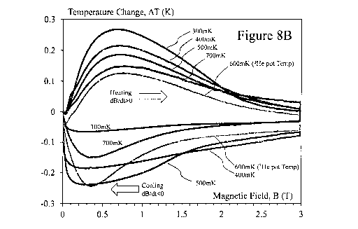
The temperature limit to magnetic cooling is set by the magnetic ordering
temperature
Tc of the spins, below which there is negligible entropy associated with the
spin degrees of
freedom. In the case of conventional paramagnetic salt refrigerants, the
ordering temperature is
set by dipole-dipole interactions ¨ 11132 11-3 . In the case of cerium
magnesium nitrate (CMN),
magnetic ordering of paramagnetic ions at an ¨lnm ion-ion distance limits
refrigeration to
2mK , see for example Pobell, and further dilution of the ion density enables
refrigeration to
0.9mK , see for example Kolk et al in "Adiabatic Demagnetization of Diluted
Cerium
Magnesium Nitrate" (J. Low Temp. Phys., Vol. 11, pp297-). A semiconductor
doped above the
critical density for a metal-insulator transition, such as the Si:As solid
state cooler within these
experiments, exhibits magnetic ordering through exchange interactions mediated
by unbound
electrons that elevate the ordering temperature Tc. Heat-capacity measurements
of heavily
doped Si have verified the importance of exchange interactions in the metallic
doping regime.
[0080]
Importantly, paramagnetic spin density is not a monotonic function of doping
density,
see Lakner and Wagner, indicating that the base temperature and cooling power
of a doped
semiconductor magnetic cooler is non-trivially dependent upon doping density.
Accordingly, the
cooling power TS1, ordering temperature Tc and thermal conductivity of the
heavily doped
silicon are all tunable with doping density.
[0081]
Accordingly, solid state semiconductor coolers according to embodiments of the
invention may be considered as providing a replacement for 'He which is a
resource of finite
- 20 -
CA 02875262 2014-12-01
WO 2013/177678 PCT/CA2013/000524
and very limited availability with a significant cost associated with it. In
contrast, silicon, is an
abundant material providing non-consumable use within ultra-low refrigeration
and cooling
applications.
[0082] As discussed above the solid state semiconductor cooling may be
applied to a variety
of semiconductor materials and semiconductor coolers may be combined for
increased cooling
capacity. Beneficially solid state semiconductor coolers may be:
= directly integrated to semiconductor substrates to cool all or a
predetermined portion of
the cryogenic electronics formed thereupon;
= directly integrated with existing cryofree technologies circumventing the
use of any
helium at all;
= have no moving parts providing increased reliability and lifetime;
= negligible preventative maintenance in discrete cooler applications;
= are very easy to use and integrate into cryogenic electronics;
= directly cool monolithically integrated devices and / or systems;
= fully compatible with semiconductor fabrication technologies; and
= have marginal cost for integrating the technology into any semiconductor
electronic
circuit.
[0083] 3. NON-DONOR SPIN COOLED SEMICONDUCTORS
[0084] Within the preceding section adiabatic demagnetization and cooling of a
semiconductor employed donor-bound spin within the semiconductor. However,
electron spin
may be bound through other effects including, but not limited to, defects and
antisite defects.
Accordingly, a semiconductor substrate or portion of a semiconductor circuit
with sufficiently
high defect density provide spin binding sites such that the adiabatic
demagnetization and
cooling may be produced in non-doped semiconductors as well as doped
semiconductors.
[0085] 4. SOLID STATE SEMICONDUCTOR COOLER APPLICATIONS
[0086] As discussed supra solid state semiconductor coolers may be directly
integrated into a
variety of cryogenic electronic devices and circuits. However, they may also
be integrated into a
variety of cryogenic photonic and opto-electronic devices. Referring to
Figures 10 through 18
-21 -
CA 02875262 2014-12-01
WO 2013/177678 PCT/CA2013/000524
examples of devices, circuits, topologies, topographies, and applications of
solid state
semiconductor cooling are presented.
[0087] Figure 10 depicts first and second transition edge sensors (TES)
1010 and 1020 which
are superconducting devices capable of counting individual photons in optical
pulses with
accuracy limited primarily by the quantum noise of the laser source. Each of
the first and second
TES 1010 and 1020 consists of a thin layer, ¨ 20nm , of superconducting
material, typically
tungsten, placed on an insulating substrate, generally silicon. In operation
each of the first and
second TES 1010 and 1020 is cooled to below the critical temperature of the
superconducting
film and a small voltage applied across the film, so that it has a slight
electrical resistance and is
in the middle of its superconducting transition region. Accordingly an
incident photon deposits
energy into the TES, heating the superconducting film and raising its
resistance such that the
photons can be detected and "counted" based upon the resistance change.
According to
embodiments of the invention first and second TES 1010 and 1020 would be
formed upon a
substrate 1030 with an insulating layer 1040 atop which the thin tungsten 1050
and interconnect
metallization 1060 are formed. According to the solid state semiconductor
substrate 1030 may be
doped or undoped wherein the insulating layer 1040 may for example be thin
oxide in the
instance of a doped silicon substrate 1030 or an intrinsic layer wherein the
semiconductor
substrate is undoped but has defect bound spins. Other variants and
alternatives would be evident
to one skilled in the art.
[0088] Optionally, the TES detectors may be formed in an array and read
with a multiplexer
based upon superconducting quantum interference device (SQUID) such as taught
by Chervenak
et al in "Superconducting Multiplexer for Arrays of Transition Edge Sensors"
(Appl. Phys. Lett,
Vol. 74, pp4043-4045). Such SQUID devices, strictly DC SQUIDs, exploit two
Josephson
junctions in parallel within a superconducting loop. Referring to Figure 11
there is depicted an
AC Josephson superconducting junction which forms part of hybrid normal-
conducting device
with an unbiased InAs nanowire as depicted in pseudo-colour scanning electron
micrograph
(SEM) 1110 and SEM image 1120.
- 22 -
CA 02875262 2014-12-01
WO 2013/177678 PCT/CA2013/000524
[0089] As depicted in cross-section X-X the InAs nanowire (NW) 1140 is
connected to three
--=250-nm-wide vanadium/titanium (V/Ti) superconducting contacts 1150 thereby
forming two
=--50-nm-1ong Josephson weak-links. Each end of the InAs NW 1140 is connected
to gold
contacts 1160 and the entire device sits upon a substrate 1170 with an
insulating layer 1180
between the substrate 1170 and hybrid normal-conducting device in the
instances that the
substrate 1170 is conducting. Accordingly localized solid state cooling may be
applied by the
substrate 1170 to the hybrid normal-conducting device or alternatively
localized heating may be
applied from the insulating layer 1180 in other embodiments of the invention.
[0090] Referring to Figure 12 there are depicted a quantum bit memory cell
1210 and
superconducting interconnection structure 1220. Quantum bit memory cell 1210
operates based
upon rapid super-flux quantum (SFQ) technology wherein digital data is carried
by magnetic
flux quanta are produced by Josephson junctions instead of transistors in
semiconductor
electronics and wherein the magnetic flux quanta are carried by picosecond-
duration voltage
pulses that travel on superconducting transmission lines, instead of static
voltage levels in
semiconductor electronics. Accordingly quantum bit memory cell consists of a
quantum bit
memory loop (Qu-bit) 1250 comprising 50nm Josephson Junctions (JJs) which is
accessed
through a control line 1230. Adjacent to the Qu-bit 1250 is a readout SQUID
1240 comprising a
pair of 100nm JJ devices such that overall a single bit has an area of
approximately 2 m square.
[0091] A memory array of Qu-bit 1250 devices may be implemented in layers M8
and M9 of
a superconducting interconnection structure 1220 for example upon a silicon
substrate together
with ground plane M7, DC power planes M1 and M2, and first and second passive
transmission
lines (PTLs) formed within layers M3 through M6. Accordingly as evident from
discussions
-23 -
CA 02875262 2014-12-01
WO 2013/177678 PCT/CA2013/000524
supra in respect of solid state cooling on silicon and other semiconductors it
would be evident
that such Qu-bit memory devices as well as other Qu-bit circuits may be cooled
exploiting
embodiments of the invention. Layers M1 through M9 may for example be niobium
or another
metal providing superconducting behaviour at the operating temperature of the
cooler.
[0092] Referring to Figure 13 there is depicted a superconducting 2' order
bandpass sigma-
delta analog-to-digital converter (2" EA ADC) according to Kirichenko in US
Patent
Application 2010/0,026,537 entitled "Superconductor Analog-to-Digital
Converter" wherein a
pair of resonators are employed but only the second stage has an explicit
feedback loop, the first
stage feedback being implicit. The comparator is JJ2 which is clocked through
JJ1 such that
comparator JJ2 subtracts a single flux quantum from the input while producing
a digital output
SFQ pulse, and thus, provides for the implicit feedback. The signal to be
digitized is being
received by the Resonator 2 whilst Resonator 1 feeds into the comparator JJ2
thereby generating
SFQ pulses, which are directed to the feedback loop and to the ADC digital
output.
[0093] The coupling between the two resonators is accomplished through a
SQUID amplifier
and Josephson transmission line (JTL) so as to provide non-reciprocal,
directional, coupling
between Resonator 2 and Resonator 1. The SQUID amplifier being inductively
coupled to
Resonator 2. Accordingly the 2" EA ADC may exploit a similar stacked
metallization and
interconnection structure as represented by superconducting interconnection
structure 1220 in
Figure 12 and exploit solid state semiconductor cooling as discussed above
using doped or
undoped semiconductor substrates or thin films.
[0094] Referring to Figure 14 there is depicted a self-assembled silicon-
germanium (SiGe)
nanocrystal grown directly on Si by molecular-beam epitaxy via Stranski-
Krastanow growth
mode. These nanocrystals can have a variety of sizes and shapes and their
composition can be
controlled to a high degree by adjusting the growth parameters. In addition,
their positions can be
controlled via pre-patterning of the growth surface. SiGe nanostructures can
form ideal contacts
with metals, which is essential for making hybrid superconductor-semiconductor
devices. As
depicted in Figure 14 the smaller contact area between drain and source
electrodes in conjunction
with the lower dimensionality of self-assembled SiGe nanocrystals extends gate
control of the
supercurrent to the single-hole level. Self-assembled SiGe nanocrystals in
such configurations
may support two-dimensional Qu-bit architectures in quantum information
applications as
- 24 -
CA 02875262 2014-12-01
WO 2013/177678 PCT/CA2013/000524
opposed to one-dimensional architectures based on Ge/Si core/shell nanowires
for example. As
depicted in Figure 14 the SiGe nanocrystals are formed upon a stack comprising
undoped silicon,
silicon dioxide, and heavily doped silicon. Accordingly embodiments of the
invention provide
for solid state cooling to be implemented within the undoped silicon and / or
doped silicon
substrate portions.
[0095] Referring to Figure 15 there is depicted a dot-within-a-dot-in-a-
nanowire light source
1500 comprising a substrate 1510, for example n-type <111> silicon, upon which
a GaN buffer
1520 is grown, followed by three vertically aligned large quantum dots 1540
within GaN barrier
1530, and a GaN capping layer 1550. An ITO electrode 1560 is formed on top of
the GaN
capping layer 1550 to provide the top electrode to the dot-within-a-dot-in-a-
nanowire light
source 1500. Due to the very high quality, relatively defect free, and uniform
growth within the
quantum well and quantum dots localized In rich nanoclusters form within each
quantum dot as
it is grown, thereby forming small quantum dots 1545 within each of the large
quantum dots
1540. As depicted the substrate 1510 is formed upon a base 1570 and as
discussed supra in
respect of embodiments of the invention the substrate 1510 and / or base 1570
may be doped or
undoped and provide semiconductor solid state cooling according to embodiments
of the
invention. It would also be evident that the nanowire may also form part of
the overall solid state
cooling based upon embodiments of the invention.
[0096] Now referring to Figure 16 there is depicted a transfer method for
semiconductor
nanotubes. Pseudomorphic InGaAs/GaAs quantum dot heterostructures were grown
on GaAs
substrates, which consist of a 50nm AlAs sacrificial layer 1611 and 20nm
In0.18Ga0.82As
1614B and 30nm GaAs layers 1614A. Two In0.5Ga0.5As quantum dot layers were
embedded in
the GaAs matrix, not shown for clarity. The use of quantum dots can
substantially reduce
nonradiative recombination associated with the presence of surface defects,
due to the three
dimensional localization of carriers in the dots. As shown in pre-etch
schematic 1610 a strained
U-shaped mesa was first defined by etching the GaAs 1614A to the InGaAs layer
1614B. The
AlAs sacrificial layer 1611 was also etched through at the starting edge of
the rolled-up
semiconductor tube. The self-rolling process was initiated with the selective
etching of the AlAs
sacrificial layer 1611 using hydrofluoric acid based solutions due to the
relaxation of strain in the
InGaAs/GaAs bilayer. After a certain distance, the middle part of the tube is
separated from the
-25 -
CA 02875262 2014-12-01
WO 2013/177678 PCT/CA2013/000524
substrate and as a result, continuous rolling on the side pieces leads to
freestanding
semiconductor tubes 1615 on GaAs substrate 1612 as illustrated in pre-release
schematic 1620. It
may be noted that the presence of a sinusoid corrugation at the inner edge of
the mesa results in
semiconductor tube ring resonators with an engineered geometry as will be
discussed below.
[0097]
To achieve semiconductor tube ring resonators employing semiconductor tubes
1615
on Si substrate 1616, the thin AlAs sacrificial layer underlying the mesa is
completely etched and
the fully released quantum dot semiconductor tubes 1615 are then registered on
the GaAs
substrate 1613. Subsequently, as shown in transfer schematic 1630 the GaAs
substrate 1613 is
placed directly on top of the Si substrate 1616 with the presence of an
appropriate solvent. When
the GaAs substrate 1613 is removed, freestanding semiconductor tubes 1615
preferentially stay
on the Si substrate 1616 due to the gravitational force induced by the solvent
in and around the
tube. Upon drying out the solvent the semiconductor tubes 1615 are attached to
the Si wafer
1616 by van der Waals bonding as shown in final schematic 1640.
[0098]
Referring to first and second cross-sections 1650 and 1660 respectively
structures for
semiconductor nanotubes are depicted comprising Au:Nb:Au:GaAs:InGaAs
and
Au:Nb:Au:Si:GaAs:InGaAs respectively upon Si and GaAs substrates respectively.
According to
embodiments of the invention the semiconductor layers within each of the
semiconductor
nanotubes as well as the substrates may form solid state cooling structures
depending upon
whether they are doped, therefore exploiting dopant donor spin cooling, or
undoped and
therefore defect donor spin cooling. It would be evident that in first and
second cross-sections
1650 and 1660 electrical properties of the nanotubes may be impacted by the
niobium layers in
addition to the cryogenic properties of the semiconductor layers. According to
other
embodiments of the invention nanotubes may be fabricating exploiting solid
state cooling
according to embodiments of the invention without the introduction of
superconducting and / or
additional semiconductor materials within the nanotube structure. Hence in the
instance
presented supra the nanotube may be formed solely from InGaAs/GaAs and provide
solid state
cooling itself together with that provided from the whole substrate or a
localized portion of the
substrate.
[0099]
Now referring to Figure 17 there are depicted schematics of
photoelectrochemical
device 1700A and electrobiological device 1700B respectively according to
embodiments of the
-26-
CA 02875262 2014-12-01
WO 2013/177678 PCT/CA2013/000524
invention exploiting dot-in-a-wire structures. Considering initially
photoelectrochemical device
1700A then a photovoltaic hydrogen / oxygen generator is depicted. The
photoelectrochemical
device 1700A exploiting a self-organized InGaN/GaN dot-in-a-wire photovoltaic
structure 17000
that has been grown on a low resistivity n-type Si(111) substrate 1740. N-type
Si doped GaN
1735 is formed atop this followed by vertically stacked array 1730 of quantum
dot
heterostructures, and p-type Mg doped GaN 1725. Atop this structure once
planarized upper
contacts, for example Ni/Au, that are separated by an ITO layer, ITO being
electronically
conductive and optically transparent. The bottom contact to the low
resistivity n-type Si(111)
substrate 1740 being Ti/Au, for example.
[00100] The self-organized InGaN/GaN dot-in-a-wire photovoltaic structure
17000 is then
disposed within a housing 1715 having a transparent window 1705. Adjacent the
upper ITO
layer is disposed electrolyte 1710. Accordingly, optical illumination of the
photoelectrochemical
device 1700A through the transparent window 1705, i.e. by solar radiation,
results in the self-
organized InGaN/GaN dot-in-a-wire photovoltaic structure 17000 generating a
potential across
the device such that the ITO layer and bottom layer are electrically charged
such that
electrochemical reaction occurs in the electrolyte 1710 such that for example
hydrogen is
generated. By suitable ancillary equipment around the photoelectrochemical
device 1700A these
released gases can be collected and used for energy generation. In some
instances the self-
organized InGaN/GaN dot-in-a-wire diode 17500 may be optically emissive and
the presence of
the biomolecule or other molecule being sensed may above a specific
concentration or threshold
result in the electrical characteristic being shifted sufficiently either to
result in the optical
emitter turning on or turning off. Alternatively the receptors 1780 may be
disposed upon the p-
type Mg doped GaN 1765 or in some instances the quantum dot 1770. Accordingly
by varying
the receptors 1780 across an area of the n-type Si(111) substrate 1785 and
partitioning one or
both of the upper contacts 1755 and bottom contact 1790 a compact, high
sensitivity, high
efficiency assay device may be provided.
[00101] In each instance photoelectrochemical device 1700A and
electrobiological device
1700B exploit a variety of semiconductor materials in addition to be being
grown upon
substrates which have been omitted for clarity in the descriptions with
respect to each device.
Accordingly, dependent upon their particular properties, one or more
semiconductor materials
-27 -
CA 02875262 2014-12-01
WO 2013/177678 PCT/CA2013/000524
including but not limited to the substrate may support solid state cooling
according to
embodiments of the invention.
[00102] Referring to Figure 18 there are depicted first to third stacked
assemblies 1810 to 1830
respectively according to embodiments of the invention for providing increased
solid state
cooling to a substrate or device. First and second stacked assemblies 1810 and
1820 respectively
comprise device 1840 sitting atop a stack of first to sixth cooler substrates
1850A through 1850F
respectively, but where in second stacked assembly 1820 the first to sixth
cooler substrates
1850A through 1850F respectively increase in dimensions away from the device
1840.
According to embodiments of the invention first to sixth cooler substrates
1850A through 1850F
respectively may be the same substrate, e.g. silicon, or may be different
substrates or different
combinations of substrates which may vary in at least one of material
composition, doping,
doping profile, doping pattern, geometry for example. Third stacked assembly
1830 depicts a
variant wherein a device 1860 sits atop first to third cooling elements 1870
to 1890 respectively
which as with the first and second stacked assemblies 1810 and 1820 may vary
in at least one of
material composition, doping, doping profile, doping pattern, geometry for
example but also vary
in thickness. In each of the first to third stacked assemblies 1810 to 1830
respectively the
different substrates may be bonded by one or more techniques including, but
not limited to,
direct bonding plasma activated bonding, anodic bonding, eutectic bonding,
glass fit bonding,
adhesive bonding, thermocompression bonding, and reactive bonding Accordingly
it would be
evident that solid state coolers may be designed with different operating
regimes, temperature
offsets, magnetic field ranges, etc. Also in each of the first to third
stacked assemblies 1810 to
1830 respectively the different substrates may be prepared by semiconductor
growth and
processing techniques including, but not limited to, molecular beam epitaxy,
metal-organic
chemical vapour deposition, chemical beam epitaxy, thermal evaporation,
electron beam
evaporation, atomic layer deposition, Czochralski growth, float-zone
growth/refinement, ion
implantation and thermal annealing.
[00103] It would be evident that in instances where the substrate, portion of
the substrate,
nanowire, MEMS device, or other structure being cooled generates heat, i.e.
absorbs energy (i.e.
photodetector) or dissipates power (e.g. electronics) that the solid state
cooling provided by
embodiments of the invention through adiabatic demagnetization will in many
instances be
-28-
CA 02875262 2014-12-01
WO 2013/177678 PCT/CA2013/000524
insufficient and accordingly a refrigeration cycle, analogous to the Carnot
cycle, could be
implemented. A typical process flow being depicted in Figure 19A wherein the
solid state cooler
is initially subject to an increasing magnetic flux density in step 1910
wherein the dipoles within
the solid state cooler align, thereby decreasing the solid state cooler's
magnetic entropy and heat
capacity, but as the total entropy is not reduced solid state cooler T, = To +
4TAD . Next in step
1915 in isomagnetic enthalpic transfer the added heat is removed through a
heatsink with the
magnetic field held constant to prevent the dipoles from reabsorbing the heat.
[00104] Once sufficiently cooled, the solid state cooler and heatsink are
separated in step 1920
wherein in step 1925 the magnetic field is decreased and adiabatic
demagnetization undergone
wherein an adiabatic temperature reduction occurs as the thermal entropy is
transferred to
magnetic entropy (disorder of the dipoles). Next in step 1930 isomagnetic
entropic transfer is
initiated by keeping the magnetic field constant and the solid state cooler is
placed into thermal
contact with the device being cooled. Because the solid state cooler is now at
a lower
temperature than the solid state cooler is cooler than the device heat energy
flows into the solid
state cooler. Subsequently the device and solid state cooler are separated
again and the process
loops based upon a decision in step 1940 if cooling is still required or
terminates if not. In some
instances a single cooling cycle may be sufficient whilst in others the cycle
may repeat
continuously.
[00105] It would be evident that within the process flow presented in respect
of Figure 19A the
solid state cooler, device, and heatsink are interconnected thermally in a
predetermined sequence
in order to execute the solid state cooling cycle according to an embodiment
of the invention.
Within the prior art for paramagnetic salts such interconnections have been
performed through
mechanical action(s). However, for cryogenic electronics it would be
preferable for the
interconnection of elements to be performed electrically. The thermal
properties of a
semiconductor material are like the electrical properties dependent upon
factors such as doping
and the presence / absence of carriers. Accordingly referring to Figure 19B a
solid state cooler
1970 is depicted between a heatsink 1965 and device 1945 to be cooled. Solid
state cooler 1970
comprising first and second MOS depletion elements 1950 and 1960 respectively
disposed on
- 29 -
CA 02875262 2014-12-01
WO 2013/177678 PCT/CA2013/000524
either side of substrate 1955. Each of the first and second MOS depletion
elements 1950 and
1960 respectively comprising a first contact 1980, doped region 1985 and
second contact 1990.
[00106] If, for example doped region 1985 is p-type silicon, then if a
positive voltage is applied
to first contact 1980 some of positively charged holes in the semiconductor
nearest the first
contact 1980 are repelled by the positive charge on the first contact 1980,
and exit the MOS
depletion element through the second contact 1990 resulting in a depleted
region wherein no
mobile holes remain leaving the immobile, negatively charged acceptor
impurities. If the first
contact 1980 is polysilicon of opposite type to the doped region 1985 then a
spontaneous
depletion region forms if the first contact 1980 is electrically shorted to
the doped region 1985,
in much the same manner as for a pn-junction. Accordingly under electrical
control depletion
regions may be formed within the solid state cooler 1970 adjusting the thermal
properties of the
respective regions such that though controlled electrical signaling to the
first contacts 1980
within the first and second MOS depletion elements 1950 and 1960 respectively
the device 1945,
solid state cooler 1970, and heatsink 1965 may be interconnected in the
desired sequence in
combination with the required magnetic field sequence.
[00107] As depicted device 1945 may be an active semiconductor device formed
upon a
substrate that has been processed to provide the required contacts and doped
regions in addition
to the doping region within the substrate for adiabatic demagnetization based
cooling. It would
be evident that other electrically controlled structures providing modified
thermal properties may
be implemented including, but not limited to, the alternate geometry depicted
in Figure 19C
wherein a MOSFET 19300 is formed within a substrate 19400 prior to
planarization with
planarizing material 19200 and formation of a device structure 19100, e.g. a
TES detectors, JJ,
SQUID, or nanowire for example.
[00108] It would be evident to one skilled in the art that within the
embodiments of the
invention presented in respect of Figures 1 through 19C that semiconductor
based solid state
cooling has been presented with respect to adiabatic demagnetization of spins
arising from
dopant donors and / or defects within Si primarily but that solid state
semiconductor cooling may
also be implemented within other semiconductors including, but not limited to,
Si, Ge, SiGe,
InAs, GaAs, InGaAs, AlAs, GaN, InGaN, InSb, and InP. It would be evident to
one skilled in the
art that other semiconductors may provide solid state cooling according to
embodiments of the
- 30 -
CA 02875262 2014-12-01
WO 2013/177678 PCT/CA2013/000524
invention based upon adiabatic demagnetization under appropriate material
parameters including
but not limited to, intrinsic and extrinsic semiconductors, silicon carbide,
organic
semiconductors, group IV elemental semiconductors, III-V semiconductors, II-VI
semiconductors, I-VII semiconductors, IV-VI semiconductors, V-VI
semiconductors, IT-V
semiconductors, and magnetic semiconductors.
[00109] In addition to the different families of semiconductors and specific
materials identified
above supporting semiconductor based solid state cooling via adiabatic
demagnetization of spins
arising from dopant donors and / or defects the semiconductor based solid
state cooling may be
obtained in semiconductor structures including, but not limited to, bulk
semiconductors, doped
semiconductors, undoped semiconductors, intrinsic semiconductors,
semiconductor
heterostructures, quantum wells, nanowires, quantum dots, quantum dots within
quantum dots
and / or wells, and combinations thereof
[00110] 5. NUCLEAR SPIN SEMICONDUCTOR BASED SOLID STATE COOLING
[00111] In addition to possessing electron spin the semiconductors described
and referred to
supra also possess "nuclear spin" associated with the semiconductor atoms,
such as 29S/ in
silicon and 69Ga and 75 As in GaAs for example. Correspondingly these "nuclear
spins" may be
similarly brought from a low entropy state to a higher entropy state, with
each nuclear spin flip
into an excited state taking energy from the semiconductor lattice to produce
an overall cooling.
Accordingly, demagnetization of the nuclear spin may be similarly employed to
adiabatically
cool a semiconductor in a manner similar to that with electron spin. This
nuclear spin adiabatic
cooling may be employed discretely, concurrently with electron spin adiabatic
cooling, or
sequentially with electron spin adiabatic cooling by exploiting a
demagnetization field.
[00112] It would be evident to one skilled in the art that semiconductor
structures may be
fabricated in which position and concentration of nuclear spins can be
controlled intentionally,
see for example "Isotopically Engineered Semiconductors ¨ New Media for the
Investigation of
Nuclear Spin Related Effects in Solids" (Physica E, Vol. TO, pp463-466). It
would also be
evident to one skilled in the art that within semiconductor heterostructures
nanometer-scale
polarization profiles may be achieved for nuclear spin and that it is possible
to control the local
interactions between electronic and nuclear spin with an applied voltage, see
for example Poggio
-31-
CA 02875262 2014-12-01
WO 2013/177678 PCT/CA2013/000524
et al in "Nuclear and Ion Spins in Semiconductor Nanostructures" (Physica E,
Vol. 35, pp264-
271). Accordingly localized and controlled cooling of semiconductors
exploiting nuclear spin
adiabatic demagnetization may be engineered within semiconductor devices with
or without
electron spin adiabatic demagnetization solid state cooling.
[00113] 6. CONTINUOUS CYCLE MAGNETIC SEMICONDUCTOR SOLID STATE
COOLING
[00114] There are three magnetic moments associated with an electron, one from
its spin
angular momentum, one from its orbital angular momentum, and one from its
total angular
momentum (the quantum-mechanical sum of those two components). Corresponding
to these
three moments are three different g-factors, namely the electron spin g-
factor, gõ the electron
orbital g-factor, gj, and the Lande g-factor, gj, which is defined by Equation
(17) below where
,u is the total magnetic moment resulting from both spin and orbital angular
momentum of an
electron, J = L+S is its total angular momentum, and p8 is the Bohr magneton.
' __ J (17)
[00115] Referring to Figure 20 there is depicted a schematic of the Zeeman
energy in a
heterostructure along the growth direction, z, for a semiconductor structure
consisting of a first
semiconductor material with a high g-factor, g1, at one side of the structure
and a second
semiconductor material with a low g-factor, g2 <g1, at the other side and a
graded region in
between. If electrons are made to flow from the first semiconductor material
to the second
semiconductor material in the presence of a magnetic field B such that
g1,u813>kõT
g2p8,8 < 1c8T , and the bias voltage V, <(k8T)le then the spin polarized
electrons in the first
semiconductor material are depolarized as they flow into the second
semiconductor material. In
doing so entropy, k8 in 2 per electron, and heat, geffp8B per electron is
taken up continuously
by the electrons flowing from the first semiconductor material to the second
semiconductor
material, where geff is the average g-factor where the electrons spin-flip
within the transition
region.
- 32 -
CA 02875262 2014-12-01
WO 2013/177678 PCT/CA2013/000524
[00116] Accordingly, continuous magnetic refrigeration is provided within a
semiconductor/metal heterostructure with a spatially varying Lan& g-factor, in
the presence of a
magnetic field and an electrical current supplied at an appropriate bias
voltage. The
semiconductor heterostructures can be operated either as a solid state
refrigerant in contact with
the material to be cooled, or as a solid state refrigerant monolithically
integrated into a device,
circuit or system. In both cases, magnetic refrigeration proceeds by pumping
entropy from the
matter to be refrigerated into the spin entropy of a continuously flowing
electrical current that is
initially spin polarized. Heat is extracted from the material to be
refrigerated by electron spin
flips in the constituent current, each spin flip extracting AE = g,uBB of
thermal energy, where B
is a constant bias magnetic field that may for example be applied by means of
a magnet.
[00117] Heat extraction will proceed if AR = g2,uBB is less than or of the
order of the thermal
energy kg . The bias voltage Vas. used to impart current flow should be
established such that
the Joule heating per electron eVps is less than the spin flip energy AE =
get/ ,u,B , where g is
the average g-factor at which spin flips occur. If spin flips occur primarily
within the second
semiconductor material, geff = g2, and consequently the bias voltage VD, must
be less than the
thermal voltage (lc e . The maximum heat that can be pumped per unit time
by the
semiconductor solid state refrigerator is the product of electron flow rate
and Zeeman energy, i.e.
(11e)x gpBB
[00118] It would be evident to one skilled in the art that it is known that
the Lamle g-factor for
conduction band electrons can be engineered in semiconductors and
semiconductor
heterostructures, see for example Kosaka et al. in "Electron g-factor
Engineering in III-V
Semiconductors for Quantum Communications" (Elect. Lett., Vol. 47, pp464-465).
Accordingly,
epitaxial semiconductor and / or metal growth techniques can be used to
precisely tune the g-
factor profile to effect the desired effective demagnetization that electrons
experience in moving
from the high-g first semiconductor material to the low-g second semiconductor
material.
Accordingly various g-factor profiles may be implemented and employed
including, but not
limited to, abrupt and graded heterostructure interfaces between high-g and
low-g
semiconductors and/or metals. Whilst the discussion supra is in respect of
electrons it would be
- 33 -
CA 02875262 2014-12-01
WO 2013/177678 PCT/CA2013/000524
apparent to one skilled in the art that the equivalent effect may be achieved
through spatially
varying Lande g-factor for holes and a corresponding hole flow within the
semiconductor and /
or metal heterostructure.
[00119] 7. SPATIAL MAGNETIC SPATIAL SOLID STATE COOLING
[00120] Within the preceding descriptions of magnetic cooling through spin
depolarization the
discussions and embodiments of the invention have been primarily described
from the
perspective of providing to a predetermined region of a semiconductor
structure a time varying
magnetic field from a magnetic field generator spatially fixed with respect to
the predetermined
region of a semiconductor structure. However, it would evident that
alternatively the movement
of spin from a region of high magnetic field, where spins are in a highly
polarized low entropy
state, to a region of low magnetic field, where spins are in a low polarized
high entropy state, can
also be used to effect solid state cooling according to embodiments of the
invention.
[00121] Accordingly, it would be evident that the source of magnetic field may
be of an
arbitrary shape provided that it results in the generation of suitable field
gradient in space and
time. As such the magnetic fields required for spin cooling may be generated
by a variety of
different means, including but not limited to, permanent magnets, internal
magnetic fields, DC
electromagnets, pulsed electromagnets, and superconducting electromagnets for
dissipationless
generation of magnetic field. Further, it would be evident that many
techniques for moving
magnets may be applied in combination with static or time-varying dynamic
magnetic fields to
provide the required (suitable) field gradient in space and time.
[00122] For example, it would possible to integrate within a semiconductor
structure a
microelectromechanical system (MEMS) element or elements such as, for example,
an
electrostatic actuated element, e.g. comb drives, gear, etc; resonators, e.g.
clamped beams, free
beams, plate resonators, etc; together with electrical structures such as
coils and electrodes for
example and thin film deposited rare earth magnets, such as for example those
based upon Gd,
Tb, Dy, and Nd rare earths in conjunction with Ti, V, Cr, Mn, Fe, Co, Ni, and
Cu transition
metals as reported by Yamashita et al in "Thin Film Rare Earth Permanent
Magnet, and Method
for Manufacturing the Permanent Magnet" (European Patent 1,329,912).
Accordingly, spatially
varying magnetic fields may be applied with simple characteristics, e.g.
sinusoidal with a
- 34 -
CA 02875262 2014-12-01
WO 2013/177678 PCT/CA2013/000524
resonant structure or linear with comb drive, or complex characteristics, e.g.
a comb drive with
sawtooth or other complex drive signal or an eccentric gear train.
[00123] Such structures may further be integrated with CMOS electronic such as
that described
supra in respect of Figure 19C wherein a MOSFET 19300 is formed within a
substrate 19400
prior to planarization with planarizing material 19200 and formation of a
device structure 19100,
e.g. a TES detectors, JJ, SQUID, or nanowire for example, undertaken atop the
MOSFET.
Accordingly, the MEMS structures may provide for spatially and temporally
varying magnetic
fields whilst the MOSFET 19300 through varying carrier density when operating
in depletion
mode results in electrically controlled thermal contact between the device
structure 19100 and
substrate 19400 such that the thermal contact can be "broken" by depleting the
MOSFET.
[00124] The spins yielding magnetic cooling may be carried by electrons, holes
or both species
of charge carrier simultaneously. Refrigeration by a spin current can be
thought of as Peltier
cooling via spin entropy, or spin Peltier cooling. Magnetic refrigeration
techniques can be
effected through a number of variations as the spin polarization is determined
by the product of
magnetic field and Lande g-factor. Accordingly, spin cooling may therefore be
effected not only
by the temporal and / or spatial variation of an applied magnetic field, but
also by the spatial and
/ or temporal variations of Lande g-factor. Similarly, spin polarisation based
magnetic cooling
may be effected by any simultaneous temporal and spatial variation of magnetic
field and Lande
g-factor where the net effect is to produce a spin depolarization. Generalized
spin cooling
techniques may be implemented, for example, by any combination of pulsed
magnetic fields and
arbitrarily shaped magnetic fields.
[00125] 8. MULTIPLE STAGE AND LAST STAGE MAGNETIC SOLID STATE
COOLING
[00126] Within the preceding descriptions of magnetic cooling through spin
depolarization the
discussions and embodiments of the invention have been primarily described
from the
perspective of a discrete magnetically cooled semiconductor structure.
However, spin cooling
structures (or stages) may also be combined and / or integrated together with
other spin cooling
structures / stages to increase the operating range of the magnetic cooling
based refrigerator. For
example, several spin cooling stages may be integrated in a single substrate
or in several
thermally linked substrates to widen the operating temperature range of spin
cooling.
- 35 -
CA 02875262 2014-12-01
WO 2013/177678 PCT/CA2013/000524
[00127] Similarly, spin cooling structures may also be combined and / or
integrated together
with other refrigeration techniques to widen the operating temperature range
of the composite
refrigerator. For example, single stage or multistage thermoelectric (Peltier)
cooling may be used
to bring substrate temperature to within the operating temperature range of a
spin cooling stage.
Alternatively, other prior art cooling techniques such as those based upon
vapour-compression,
vapour-absorption, gas cycles, Sterling cycles, dilution refrigerators, and
cryocoolers may be
used in conjunction with spin cooling to provide a wider operating temperature
range of the
overall refrigerator whilst achieving the very low temperatures possible
through spin cooling or
other temperature ranges as spin based cooling is applied to other materials.
[00128] Within descriptions of embodiments of the invention reference has been
made to
particular semiconductors and superconductors. However it would be evident to
one skilled in
the art that a variety of structures including but not limited to nanowires,
quantum dots, quantum
wells, nanotubes, nanorods, fullerenes, and molecular nanowires may exhibit
properties that
benefit from operation at low temperatures including but not limited to
thermal noise and band
delineation.
[00129] The foregoing disclosure of the exemplary embodiments of the present
invention has
been presented for purposes of illustration and description. It is not
intended to be exhaustive or
to limit the invention to the precise forms disclosed. Many variations and
modifications of the
embodiments described herein will be apparent to one of ordinary skill in the
art in light of the
above disclosure. The scope of the invention is to be defined only by the
claims appended hereto,
and by their equivalents.
[00130] Further, in describing representative embodiments of the present
invention, the
specification may have presented the method and/or process of the present
invention as a
particular sequence of steps. However, to the extent that the method or
process does not rely on
the particular order of steps set forth herein, the method or process should
not be limited to the
particular sequence of steps described. As one of ordinary skill in the art
would appreciate, other
sequences of steps may be possible. Therefore, the particular order of the
steps set forth in the
specification should not be construed as limitations on the claims. In
addition, the claims directed
to the method and/or process of the present invention should not be limited to
the performance of
- 36 -
CA 02875262 2014-12-01
WO 2013/177678 PCT/CA2013/000524
their steps in the order written, and one skilled in the art can readily
appreciate that the sequences
may be varied and still remain within the spirit and scope of the present
invention.
-37-