Note: Descriptions are shown in the official language in which they were submitted.
CA 02875705 2014-12-23
Doc. No. 482-03 CA
METHOD AND SYSTEM FOR PULSING AN LED LIGHT SOURCE
FIELD OF THE INVENTION
100011 The invention relates to pulsed light control, and more particularly to
a control circuit
and method for driving an LED light source for providing pulsed light.
BACKGROUND
100021 High speed photography is widely used in scientific research and in
industrial product
development. For instance, high speed imaging is a common technique that is
used for taking
images of the high pressure injection fuel spray in a combustion engine, the
development of a
shock wave, and combustion flame propagation. To improve image quality and
boost the photo
capturing speed, high intensity illumination is demanded to enhance the camera
exposure.
Typically, a pulsed laser is employed in such imaging systems for generating
transient high-
speed and high-brightness illumination, providing sufficient exposure in an
extremely short
exposure duration. Unfortunately, such pulsed lasers are far more costly than
a LED system.
[0003] The brightness of an LED is proportional to the current flow. The
maximum current is
normally limited by the LED thermal damage threshold, since high current
produces a large
amount of heat that can melt the wire joints and degrade the LED substance.
When an LED is
running in pulse mode, the transient current can exceed the continuous wave
(CW) current limit,
thereby providing brighter lighting than CW mode. The pulsed LED driving
method has been
well known for increasing the light brightness and extending LED life. Such
methods are widely
employed in LED flash lighting.
100041 However, currently available LED pulse light source products fail to
meet the high
intensity illumination requirements of high speed imaging in the previously
mentioned
application areas, largely due to the challenges of shaping the pulse for
ultra-high speed light
output. To capture an ultra-high speed motion, the illumination duration is
set in the
microseconds range. Conventional high speed LED flash lighting systems only
produce
insufficient light output at such high speed, and thus costly image
intensifiers are commonly
employed to enhance the image quality.
1
CA 02875705 2015-06-04
[0005] It would be advantageous to provide a method and system that overcomes
at least some
of the disadvantages of the prior art.
SUMMARY OF EMBODIMENTS OF THE INVENTION
[0006] It is an object of at least one embodiment of the present invention to
provide a LED
based pulsed light source, being able to generate sub-microsecond high lumens
lighting.
[0007] It is an object of at least one embodiment of the present invention to
produce high
intensity short-pulse illumination suitable for the imaging system without
employing an image
intensifier.
[0008] According to an aspect of at least one embodiment of the invention,
there is provided a
method comprising: charging a first capacitor; and providing a first pulse of
light, comprising the
ordered steps of: switching on a second transistor to discharge the first
capacitor via a first light
emitting diode having a first electrical input port and a first electrical
output port, to cause the
first light emitting diode to emit light; switching on a first transistor
coupled across the first
electrical input port and the first electrical output port, to provide a
relative potential between the
first electrical input port and the first electrical output port for stopping
the first light emitting
diode from emitting light; switching off the second transistor to stop the
discharge of the first
capacitor; and switching off the first transistor to terminate the relative
potential between the first
electrical input port and the first electrical output port of the first light
emitting diode.
[0009] According to an aspect of at least one embodiment of the invention,
there is provided a
circuit comprising: a first light emitting diode have an electrical input port
and an electrical
output port, the first light emitting diode for emitting light when electrical
current flows between
the electrical input port and the electrical output port thereof; a charge
storage component for
storing charge; a second switch for switchably releasing the charge via the
first light emitting
diode to cause light to be emitted therefrom; and a first switch for switching
the electrical input
port and the electrical output port to a relative potential therebetween, the
relative potential for
preventing the first light emitting diode from emitting light therefrom.
[0010] According to an aspect of at least one embodiment of the invention,
there is provided a
method comprising: charging a first capacitor; charging a second capacitor; at
intervals of one
2
CA 02875705 2015-06-04
period, discharging the first capacitor via a first light emitting diode
having an electrical input
port and an electrical output port to cause the first light emitting diode to
emit light; and after a
known delay substantially less than one period divided by a number of light
emission events per
period, discharging the second capacitor via a second light emitting diode
having an electrical
input port and an electrical output port to cause the second light emitting
diode to emit light; and
2A
CA 02875705 2014-12-23
Doc. No. 482-03 CA
switching a transistor coupled across the electrical input port and the
electrical output port of the
second light emitting diode to stop the light emitting diode from emitting
light.
[00111 According to an aspect of at least one embodiment of the invention,
there is provided a
circuit comprising: a first capacitor; a second capacitor; a first light
emitting diode having an
electrical input port and an electrical output port; a second light emitting
diode having an
electrical input port and an electrical output port; at least a control
circuit for controlling
charging of the first capacitor and the second capacitor and for at intervals
of one period,
discharging the first capacitor via the first light emitting diode to cause
the first light emitting
diode to emit light for forming a light emission event and after a known delay
substantially less
than one period divided by a number of light emission events from the circuit
per period,
discharging the second capacitor via the second light emitting diode to cause
the second light
emitting diode to emit light to form another light emission event; a first
transistor coupled across
the electrical input port and the electrical output port of the first light
emitting diode to stop the
first light emitting diode from emitting light; and a third transistor coupled
across the electrical
input port and the electrical output port of the second light emitting diode
to stop the second light
emitting diode from emitting light.
[0012] According to an aspect of at least one embodiment of the invention,
there is provided a
lighting circuit comprising: a first light emitting device; a charge storage
component for storing
charge; and a control circuit for sensing a voltage across one of the first
light emitting device and
the charge storage device to provide sensed voltage and, in dependence upon
the first light
emitting device, feedback current and sensed voltage, automatically
controlling a charge voltage
on the charge storage component and a duration of a discharge of the charge
storage through the
first light emitting device.
BRIEF DESCRIPTION OF THE DRAWINGS
100131 The instant invention will now be described by way of example only, and
with reference
to the attached drawings, wherein similar reference numerals denote similar
elements throughout
the several views, and in which:
100141 Figure 1 is a sketch diagram of a light emitting diode driving circuit
for driving a light
emitting Diode LED.
3
CA 02875705 2014-12-23
Doc. No. 482-03 CA
[0015] Figure 2 is a simplified timing diagram of a method of switching the
MOSFETs Q1 and
Q2.
[0016] Figure 3 is a sketch diagram of another light emitting diode driving
circuit for driving a
light emitting Diode LED.
[0017] Figure 4 shows a control sequence and synchronization of a light source
and camera
during image recording.
[0018] Figure 5 is a simplified block diagram of a light emitting diode light
source.
[0019] Figure 6 shows a layout of the light source comprising multiple LED
drivers.
[0020] Figure 7 illustrates the operation modes of multiple light emitting
diodes.
[0021] Figure 8 shows several supported light emitting diode array
configurations.
[0022] Figure 9 shows a simplified timing diagram for a double shot
implementation.
[0023] Figure 10 is a representation of a photographic image of a shock wave
captured using
shock wave Schilieren imaging by means of two different camera modes.
DETAILED DESCRIPTION OF EMBODIMENTS
[0024] The following description is presented to enable a person skilled in
the art to make and
use the invention, and is provided in the context of a particular application
and its requirements.
Various modifications to the disclosed embodiments will be readily apparent to
those skilled in
the art, and the general principles defined herein may be applied to other
embodiments and
applications without departing from the scope of the invention. Thus, the
present invention is not
intended to be limited to the embodiments disclosed, but is to be accorded the
widest scope
consistent with the principles and features disclosed herein.
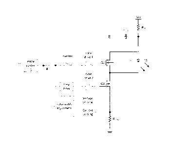
[0025] Referring to Figure 1, shown is a sketch diagram of a light emitting
diode driving circuit
for driving a light emitting Diode LED. A capacitor in the form of external
capacitor CExr is
charged by a power supply Vcc via an external resistor RExT. The capacitor and
resistor are
typically external, but optionally are integrated with the driver circuit. The
capacitor CExT is
4
CA 02875705 2014-12-23
Doc. No. 482-03 CA
located close to light emitting diode LED, in order to reduce overall
resistance between the
capacitor CExT and the light emitting diode LED.
[0026] Two fast switching MOSFETs Q1 and Q2 within the light emitting diode
driver circuit
support switching so as to pulse energy through the light emitting diode LED.
Low side
MOSFET Q2 actuates turning-on of light emitting diode LED, while high side
MOSFET Q1
actuates turning-off of light emitting diode LED. As is seen in the figure,
when low side
MOSFET Q2 is not conducting and high-side MOSFET Q1 is not conducting, energy
from Vcc
charges capacitor CExT but there is no current flow path through the light
emitting diode LED.
When low side MOSFET Q2 is conducting and high-side MOSFET Q1 is not
conducting, energy
from capacitor CExT flows to ground via light emitting diode LED, low side
MOSFET Q2 and
resistor RSENS, causing light emitting diode LED to emit light. When low side
MOSFET Q2 is
conducting and high-side MOSFET Q 1 is conducting, energy from capacitor CExr
can still flow
to ground, for example via high side MOSFET Q I, low side MOSFET Q2, and
resistor RSENS but
does not flow through the light emitting diode LED as both poles of the light
emitting diode LED
are coupled via high side MOSFET Ql. So long as the voltage drop across MOSFET
Q1 is less
than the voltage for switching the light emitting diode LED into a light
emitting state, the diode
is forced into an off state by turning on high side MOSFET Ql.
[0027] Figure 2 is a simplified timing diagram of a method of switching the
MOSFETs Q1 and
Q2. Here, a command sequence for the two MOSFETs Q1 and Q2 is shown.
Basically, in this
embodiment, Qland Q2 are commanded approximately oppositely with a short phase
shift
introduced between the opposite signals. Initially, high side MOSFET Q1 is
engaged to equalize
the potential between the two terminals of the light emitting diode LED,
thereby ensuring that
light emission does not occur from light emitting diode LED. High side MOSFET
Q1 is then
switched OFF, into a non-conducting state, at ti. After a predetermined short
delay ¨ the phase
shift, low side MOSFET Q2 engages at t2 and causes light emitting diode LED to
emit light.
High side MOSFET Q1 engages again at t3 thereby equalizing terminals of the
light emitting
diode LED and switching the light emitting diode LED into a mode where it does
not emit light.
The light emitting diode LED light output duration is thus determined by t3-
t2. Low side
MOSFET Q2 is then switched off starting at either t3 or t4. Such a process
provides excellent
control of light pulse timing both for switching the light on and for
switching the light off ¨
CA 02875705 2014-12-23
Doc. NO. 482-03 CA
controlling the pulse duration. The process is repeatable, and for pulsed
light the process is
repeated at a known frequency.
[0028] Advantageously, a dual MOSFET driving methodology and circuit as
presented allows
for shaping of emitted light pulses. The light emitting diode is driven in
overcurrent - up to 300A
in transient - to generate high lumen output light. Handling switching of high
current relies upon
high performance MOSFETs and optimized circuit board design. With current
state-of-art
MOSFETs and matched gate drivers, switching rise time is fast enough to
support a sharp rise of
intensity for output light. Unfortunately, cutting off high current may
generate undesired
oscillation affecting switching from emitting light to a mode where light is
not emitted. The
function of Q1 offers fast turn-off of light emitted from light emitting diode
light and eliminates
uncertainties during transition; the transition from light emitting mode to a
mode where light is
other than emitted relies on equalization of potential across the light
emitting diode - two poles
of the light emitting diode are at a same or similar potential, thereby
forcedly cutting off current
across the light emitting diode. This provides improved timing control and is
useful for capturing
of some images.
[0029] Referring to Figure 3, shown is a sketch diagram of another light
emitting diode driving
circuit for driving a light emitting Diode LED. Two external capacitors are
series connected to
provide a voltage reference; typically half of the power supply voltage when
two identical
capacitors are employed. One of the LED poles is connected to the voltage
reference between the
two capacitors, and the other pole is connected between the two MOSFETs. The
driving scheme
is similar to the figure 2. At ti, when the MOSFET Q 1 is conducting and Q2 is
not conducting,
the LED is at reverse state (the negative pole of the LED has higher potential
than the positive
pole), and thus there is no current flow. At t2, the MOSFET Q1 is not
conducting and the Q2 is
conducting, the energy in the two external capacitors discharge through the
LED and the LED
emits light. At t3, the MOSFET Q1 turns on and raises the potential at the LED
negative pole,
when the potential at the LED negative pole becomes higher than the potential
at the positive
pole, the LED stops emitting light. The LED light emitting duration is
determined by t2 and t3.
At t4, the MOSFET Q2 turns off and there is no current flow through either LED
or MOSFET.
The LED can be configured at a different polarization; correspondingly, the
two MOSFETs
should be driven in the opposite sequence to that shown in figure 2. In this
diving scheme,
6
CA 02875705 2014-12-23
Doc. No. 482-03 CA
instead of equalizing the potential between the LED to turn off the light
emitting, the LED on/off
is controlled by electrically pulling up/down one pole of the LED. A fast
recovery diode is
connected to the negative pole of the LED for over voltage protection.
[0030] Figure 3 shows a control sequence and synchronization of the light
source and a camera
during image capture. The camera operates in high-speed mode, with an exposure
period
covering the light emitting diode's light emitting time. Each image frame
records a phenomenon
at a time illuminated by a light emission within a strobed light emission.
Thus, very sharp
images, even of fast moving items, can be captured. In another camera mode, a
longer exposure
time covering multiple light emitting diode light emitting events is used
allowing for
superposition within a single frame of several "snapshots" in time.
Progression of a physics
phenomenon is recoded in successive frames in the first mode and in one image
frame in the
second mode. This, for instance, allows measurement of flame propagation,
shock wave fronts,
spray development processes, and many other transient processes for
visualization. Sharp
shaping of light pulse with a fast rise time and a fast fall time across the
light emitting diode, and
high speed of a light pulse both for accuracy of timing and for pulse
duration, is sometimes
critical for visual descriptions of these crucial developments and formations.
[0031] Referring to Figure 4, shown is a simplified block diagram of a light
emitting diode light
source. The block diagram is for a programmable light source and includes
programmable
control IC. The programmable IC generates control signals for switching the
low side MOSFET
Q2 and the high side MOSFET Q1 within the LED Driver block. The LED driver
block includes
light emitting diode(s), charge storage in the form of capacitors, a power
source and Q1 and Q2.
Alternatively, the LED driver includes a power port for receiving external
power therefrom. As
shown, the LED driver includes a feedback path to provide the programmable
control IC with
information about charge on the charge storage. The intelligent control unit
includes a
communication interface for communicating with the programmable control IC as
well as other
circuitry such as a trigger circuit, a timer circuit, a conditioning circuit
for signal conditioning
and an optional display. The trigger circuit and the timer circuit act to
determine pulse spacing
and width to provide both frequency and duty cycle control. Alternatively, the
trigger circuit and
the timer circuit act to determine pulse spacing and width and interleaving to
provide frequency,
7
CA 02875705 2014-12-23
Doc. No. 482-03 CA
duty cycle, and in period on-off characteristic control. Of course, the same
circuitry also supports
single pulses, for example for flash photography.
[0032] Control signals for triggering - for driving - the MOSFETs optionally
are provided from
a same pulse width modulation (PWM) module. As shown in Figure 1, when a pulse
such as that
shown in Figure 2 is used, the signal is provided from the PWM and the second
signal Q2 is
inverted and delayed. Alternatively, the signal provided is delayed to form
the signal for Q2 and
inverted to form the signal for Q 1 . Alternatively, each signal for driving
Q1 and Q2 are
generated separately. Further alternatively, the signal for Q1 triggers the
signal for Q2. Because
the delay ¨ the phase shift ¨ is circuit dependent, it has a range of values
supported but does not
need to be adjusted for a given frequency. Thus, once the delay is determined
for a circuit, the
same delay is applicable at all frequencies of operation for that circuit
given that the delay does
not render the circuit non-functional.
[0033] In an embodiment, voltage and current sensing signals are connected to
a pulse width
adjustment module. Pulse width is then adjusted based on predetermined thermal
damage
thresholds, thereby protecting the light emitting diode LED. Of course, when
the predetermined
thermal damage thresholds are unchanging, the pulse width is optionally
designed into the circuit
in a fixed fashion. When the predetermined thermal damage thresholds vary over
time, providing
a pulse width adjustment module allows for pulse width changes in response to
changing
thresholds. In some embodiments, a fast recovery diode (shown in Figure 1 in
shadow) is
reversely paralleled to the light emitting diode LED to cancel the reverse
high voltage during the
action of MOSFETs, protecting the light emitting diode LED from the high
voltage damage.
[0034] An embodiment of the light source comprises several functions for
intelligent control
and supporting a user-friendly interface. This is discussed with reference to
Figure 4. A variable
voltage module is employed to regulate flexibly a capacitor charging voltage
in order to support
different light emitting diodes and in order to meet requirements of varied
current levels at
various pulse widths. When pulse duration is shortened to enhance imaging
speed, more light
lumens is often demanded and achievable through augmenting current. The
shorter the pulse
duration, the higher the current that can be applied across the light emitting
diode without likely
damaging the light emitting diode. Transient current is determined based on
voltage applied
8
CA 02875705 2014-12-23
Doc. No. 482-03 CA
across the light emitting diode, since resistance along a current path is
often fixed with the circuit
layout. Thus voltage is set for a given pulse width to provide optimal output
light according to
imaging or other needs. The module also includes a circuit for draining the
charge storage device
in the form of the capacitor to reduce capacitor voltage if and when a lower
voltage is needed.
Alternatively, increased lumens are provided by increasing a number of light
emitting diodes that
are driven simultaneously.
[0035] The programmable control IC is adapted for intelligent control of
voltage and PWM. In
an embodiment, a voltage to pulse width relation is pre-set in the control IC
to automatically
adjust the voltage according to the pulse width setting. Alternatively, both
the pulse width and
voltage are programmable. For the purpose of optical alignment, the voltage
can be set at a low
voltage which allows continuously low intensity light emitting without
overheating the LED.
The voltage and current are sensed and fed back to the control IC for further
refinement. There is
also a current to pulse width relation defining a maximum current threshold.
In the presented
embodiment, whenever an undesired high current spike occurs and exceeds a
predetermined
duration, MOSFET Q1 engages to protect LED.
[0036] The light emitting diode is a single high lumens light emitting diode.
Alternatively, an
array of light emitting diodes having a total lumen output brightness to meet
specified
requirements is provided. In the diagram of Figure 4, the light source has a
communication
interface in the form of a universal serial bus interface (USB) for connecting
to a personal
computer (PC) or other terminal for programming and setting the controller.
[0037] A timer circuit is embedded in the intelligent control unit, serving as
the internal clock
for pulse width modulation generation and signal synchronization. An input
trigger signal for the
circuit has two triggers - one is from an external user-defined TTL pulse and
another is generated
by a push button. The input trigger signal is then processed by a signal-
conditioning unit for
eliminating signal errors. For example, the signal is subject to debounce
filtering to prevent one
button press from registering as multiple button presses in rapid succession.
Based on the
internal timer clock, the control unit refines the signal so that the light
source is more
accommodating to differing input signal quality. In addition to pre-set or
controllable parameters
through PC software, an onboard input port and display unit is employed to
receive and display
9
CA 02875705 2014-12-23
Doc. No. 482-03 CA
settings of the parameters as they currently stand. Alternatively, the circuit
communicates with
another computer for providing an indication of the parameters and an
opportunity to modify
said parameters.
[0038] The light source is also configurable to operate multiple light
emitting diodes. By
positioning light emitting diodes in predetermined patterns or, alternatively,
close together, a
plurality of light emitting diodes is switched to emit light simultaneously,
thereby increasing
output light without increasing current flowing through a single light
emitting diode. Figure 5
shows a layout of a light source comprising multiple light emitting diode
drivers ¨ each light
emitting diode is shown with its own driver. Alternatively, a single driver
drives more than one
light emitting diode. In the configuration of Figure 5, a control unit
receives a start-up trigger
signal and in response thereto distributes control signals to multiple light
emitting diode drivers
for driving each light emitting diode separately but with related timing This
configuration
supports simultaneous light emission or closely strobed light emission,
wherein some driver
circuits switch a light emitting diode shortly after others.
[0039] Figure 6 illustrates the operation modes of multiple light emitting
diodes. In light
emitting diode mode A, the multiple light emitting diodes are operated with a
synchronized
schedule such that all light emitting diodes emit light simultaneously; the
overall light intensity
of each individual flash event is thus multiplied. In light emitting diode
mode B, one light
emitting diode (or a group of synchronized light emitting diodes) emits light
during the dwell of
another light emitting diode (or a group of synchronized light emitting
diodes). The overall
illumination frequency is doubled or a pattern of illumination is thereby
created but the emitted
light intensity is only that of the light emitting diodes that emit light
simultaneously.
Alternatively, three or more groups of light emitting diodes are used. More
groups of light
emitting diodes allows for increased frequency without increased current to
each light emitting
diode or for more complex patterns of light emission.
[0040] For high lumens light emitting diodes that operate in overcurrent pulse
mode, there are
two common causes of damage. A first one is fusing of bond wires due to the
current overflow;
this occurs when current exceeds a certain threshold. A second one is non-
reversible degradation
due to high repetitive frequency that sometimes happens even while maintaining
a current lower
CA 02875705 2014-12-23
Doc. No. 482-03 CA
than the threshold current. Configuring the lighting circuit with multiple
light emitting diodes is
beneficial for preventing or reducing a likelihood of each of these sources of
light emitting diode
damage. That said, multiple light emitting diodes increases an area on a
semiconductor that is
used and, as such, a cost benefit trade-off exists.
[0041] Another method for use of the above noted control circuitry supports
different operating
modes of the light emitting diode. Figure 7 shows several supported light
emitting diode array
layouts. In a single driver configuration, the light emitting diodes are
either series or parallel
connected, shown in Figure 7 (a) and (b), respectively. For these layouts, the
light emitting
diodes are operated simultaneously, in Mode A of Figure 6. That said, each
configuration has
advantages and disadvantages relative to the control circuit as will be
understood by those of
skill in the art. In a separated layout shown in Figure 7 part (c), the light
emitting diodes are
mounted closely but isolated one from another and each light emitting diode is
driven and
controlled separately. Of course, the term closely depends on the application
within this layout.
For example, the light emitting diodes are operated in either synchronization
Mode A or B of
Figure 6. Since the size of a high lumens light emitting diode is only several
square
millimeters, the layout of a few light emitting diodes is still relatively
small and compact. Thus
the light emitting diode array is positioned to share a same optical lens for
converging or
collimating light emitted therefrom. Alternatively, the light emitting diodes
are positioned in a
configuration dictated by design or other requirements. For example, they are
disposed in a ring
for disposal about a camera lens.
[0042] The circuit described supports external control thereof. For example,
pulse width is
adjustable as is pulse period. When multiple light emitting diodes are used on
a single circuit,
each fired by separate control circuitry, the control circuitry can be
synchronized to support
faster strobing through cycling through different light emitting diodes for
each pulse ¨ for
example doubling the frequency has half the diodes light up and then the other
half for providing
strobe lighting with same period between light emission. Alternatively, the
period between light
emitting events of different groups of light emitting diodes is also
controllable. In this fashion,
the light source can be operated as a single-shot ¨ only one group of light
emitting diodes
lighting each period or two groups of light emitting diodes lighting at once,
as a double-shot -
with two groups of light emitting diodes lighting one immediately after
another to provide two
CA 02875705 2014-12-23
Doc. No. 482-03 CA
strobes closely offset, and a repetitive-pulse mode ¨ where groups of light
emitting diodes
alternate with a consistent period between lighting emissions. Timing for a
double shot
implementation is shown in Figure 8. Relying on double shots with the control
circuitry
synchronized one to another, an imaging technique where two strobed lighting
events are
superimposed within a single camera frame is achievable. As the double shot is
optionally
repeated at a known frequency, double shot strobe lighting is supported
allowing for multiple
sequential double-shots within each sequential camera frame period. This is
useable for high
speed Particle image velocimetry (PIV) measurement and other velocity related
measurement.
[0043] Figure 9 is an image captured using a multiple shot strobe lighting
source according to at
least an embodiment described above. As noted, multiple shock wave fronts ¨
the shock wave
front at multiple locations are captured within a single image in mode B.
[0044] Numerous other embodiments may be envisaged without departing from the
scope of the
invention.
12