Note: Descriptions are shown in the official language in which they were submitted.
WO 2013/120580
PCT/EP2013/000214
1
Device for contacting a circuit board
The invention relates to a device for contacting a
circuit board which is to be connected, at least temporarily,
with, for example, a measuring device or a circuit of any
kind.
At present it is known for such circuit boards to be
contacted by plugging on one or more connector heads, which,
however, is generally associated with the disadvantage of
requiring a relatively large plugging force, which
substantially results from the mechanical locking of the
connector heads by means of spring elements. A contacting by
means of connector heads is therefore unsuitable, at least in
the case of circuit boards with flexible carrier plates.
Moreover, connection errors can result from the plugging of
the individual connector heads which can lead to damage to the
circuit board or to the electrical system connected to it.
Starting out from this prior art, the invention was based
on the problem of describing a device which makes possible a
simple, quick contacting of a circuit board and in particular
avoids the application of high plugging or contact forces, so
that damage to the circuit board can be avoided even if the
circuit board is based on a flexible carrier plate.
CA 2876631 2017-12-08
CA 02876631 2015-01-06
WO 2013/120580 PCT/EP2013/000214
2
The invention is based on the idea of contacting a
circuit board with matching contacts quickly, securely and in
particular with the application of lo* contact forces, in that
the circuit board or the corresponding section of the circuit
board which is to be contacted is fixed in an intake and a
contacting of the circuit board and contact elements is then
effected through a guided movement or sliding of the circuit
board or of the relevant section, preferably fixed in the
intake.
Accordingly, a device according to the invention for
contacting a circuit board comprises at least the following
elements:
- one or more contact elements, which are preferably
positioned immovably in the device and are in particular
arranged within a (part of a) housing of the device;
- (at least) one intake, into which at least one
section of the circuit board can be inserted; the intake
preferably embraces the circuit board or the section of the
circuit board over as wide an area as possible and in
particular only leaves exposed the section of the circuit
boards on which those (sections of the) circuit paths are
arranged which are to be contacted;
- means for moving or sliding the circuit board
relative to the contact elements until a contacting with the
contact elements takes place; the guided movement of the
circuit board ensures that this moves towards the contact
elements in a defined manner, which rules out contacting
errors and moreover prevents the circuit board from tilting
relative to the contact elements, as could occur where
higher contact forces are used; and
- means for fixing or retaining the circuit board in
the position in which the contact elements are contacted,
ensuring permanent contacting.
CA 02876631 2015-01-06
WO 2013/120580 PCT/EP2013/000214
3
In a preferred embodiment of the device according to the
invention, the device also possesses (at least) one centring
element through which the circuit board is centred prior to
the contacting of the contact elements. This is preferably
achieved through the guided movement or sliding of the circuit
board relative to the contact elements.
For example, (at least) one centring pin (preferably
tapering in at least one section) can be provided onto which
an opening in the circuit board is pushed, causing it to be
centred. In this way it can be ensured that the circuit paths
of the circuit board are aligned exactly in relation to the
corresponding contact elements.
Particularly preferably, at least two centring pins can
be provided which differ in terms of their form, arrangement
and/or dimensioning and can engage in correspondingly arranged
and/or dimensioned openings in the circuit board. This can
create a coding which allows an incorrect insertion of the
circuit board to be prevented.
Preferably, the circuit board can be moved or slid
together with the intake in order to contact the contact
elements. This makes it possible to apply the forces necessary
for the movement to the intake and not to the circuit board.
The transmission of these forces from the intake to the
circuit board can then take place over a relatively large
surface area and consequently with less pressure.
Also preferably, the intake can be spring-mounted. This
means, on the one hand, that in its unloaded state, i.e. when
it is not subjected by the means for sliding to a force
causing movement, the intake is biased by the spring-loaded
mounting into an initial position in which the circuit board
does not contact the contact elements. This makes it possible
to ensure that, on being plugged into the intake, the circuit
board does not yet establish a contact with the contact
CA 02876631 2015-01-06
WO 2013/120580 PCT/EP2013/000214
4
elements. The sliding of the circuit board including the
intake with the aim of contacting the contact elements can
then take place against the opposing force of the spring-
loaded mounting of the intake. The resulting pre-tensioning of
the spring can, in addition, be used to fix the circuit board
in the position in which the contact elements are contacted
(contact position).
The sliding of the circuit board can preferably be
effected by means of a slider, whereby the directions of the
movement of the slider and the movement of the circuit board
are preferably non-parallel (also non-coaxial). This non-
parallelism of the movements of slider and circuit board has
the advantage that a relatively large transmission ratio can
be realised by simple means, so that a significantly greater
sliding movement of the slider is necessary in order to effect
the preferably relatively short movement of the circuit board
from the initial position into the contact position. This
facilitates the handling of the preferably manually operated
slider.
The non-parallel movements of slider and circuit board
can be achieved in a simple manner in that a contact surface
of the slider slides on a contact surface of the circuit board
and/or the intake, whereby, with respect to the direction of
the relative movement, the contact surfaces are aligned at an
angle of between >0 and <90 relative to one another. This
means that the desired non-parallel movements of slider and
circuit board can be realised in a simple manner,
corresponding to the function of an "inclined plane". In
addition, the transmission ratio of the two movements can be
adjusted simply through the selection of the angle formed
between the contact surfaces.
Furthermore, a force-locking fixing of the slider in the
position in which the circuit board contacts the contact
CA 02876631 2015-01-06
WO 2013/120580 PCT/EP2013/000214
elements can be realised through this embodiment. This can be
achieved in that the travel of the circuit board, as a result
of the movement of the slider, takes place against the
resilient force of a spring element. This resilient force can
increase the friction between the two contact surfaces and
consequently make possible a force-locking fixing of the
slider in the contact position of the device. The elastic
resilient forces can for example be applied by the spring-
loaded mounting of the intake if the intake is displaced
together with the circuit board. Alternatively or in addition,
the advantageous possibility also exists of having the
resilient forces applied by the contact elements, for example
in that these are spring-mounted or generate the resilient
forces themselves as a result of deformation.
In a preferred embodiment of the device according to the
invention, this can possess a housing comprising a first
housing part forming the intake and a second housing part
containing the contact elements, whereby the two housing parts
can be moved relative to one another.
The two housing parts can particularly preferably be
designed so as to rotate relative to one another and can in
particular be connected with one another in such a manner,
whereby in a first rotary position a circuit board plugged
into the intake contacts, or would contact, the contact
elements and in a second rotary position a circuit board
plugged into the intake does not contact or would not contact
the contact elements.
Also preferably, the two housing parts are biased in the
first rotary position by means of a spring element. In order
to plug in the circuit board, the two housing parts are then
rotated relative to one another into the second rotary
position (for example manually), so that the circuit board can
be plugged in without contacting the contact elements. A
CA 02876631 2015-01-06
WO 2013/120580 PCT/EP2013/000214
6
release of the two housing parts can then lead to the two
housing parts being automatically moved into the first rotary
position as a result of the spring force and fixed in this
position through the spring force.
Since plugging the circuit board into the intake in the
first rotary position could damage the contact elements and/or
the circuit board, means can also preferably be provided which
prevent the circuit board from being plugged into the intake
in the first rotary position. These means can preferably
consist of the centring pin or pins which, in the first rotary
position, are arranged in an insertion slot of the intake and
consequently prevent the circuit board from being plugged into
the intake.
In a further preferred embodiment of the device according
to the invention, at least one HF contact element can be
provided for the transmission of high frequency signals and at
least one DC contact element can be provided for the
transmission of direct current. The HF contact element can
thereby advantageously comprise a central contact part which
is arranged in a coplanar alignment between two outer contact
parts.
Since coaxial cables are advantageously suitable for the
transmission of high frequency signals, the central contact
part can also preferably be electrically connected with an
inner conductor and the outer contact parts can be
electrically connected with an outer conductor of a coaxial
cable leading away from the device. The device or the HF
contact elements can, for example, be connected with a
measuring device by means of the coaxial cable.
In contrast, the DC contact element can, advantageously,
be electrically connected with a preferably flexible ribbon
conductor leading away from the device. These can be
distinguished through low costs and a low space requirement. A
CA 02876631 2015-01-06
WO 2013/120580 PCT/EP2013/000214
7
direct contacting to one or more stranded copper conductors is
also possible.
The contacting of the circuit board with the contact
elements of the device according to the invention is, in
particular, intended to allow high frequency signals (HF
signals) to be transmitted.
The invention is explained in more detail in the
following with reference to exemplary embodiments illustrated
in the drawings, in which:
Fig. 1 to Fig. 3: show different steps in the use of a
first embodiment of a device for contacting a circuit board in
accordance with the invention;
Fig. 4: shows a section of the device according to Figs.
1 to 3 in an isometric longitudinal section;
Fig. 5: shows an isometric view of an intake element of
the device according to Figs. 1 to 4;
Fig. 6: shows a perspective view of a second embodiment
of a device in accordance with the invention (without circuit
board) in its closed state;
Fig. 7: shows the device according to Fig. 6 in its
closed state;
Fig. 8: shows a perspective view of a circuit board for
use with the device according to Figs. 6 and 7;
Fig. 9: shows a perspective view of the device according
to Fig. 6 and 7 with partially inserted circuit board
according to Fig. 8;
Fig. 10: shows a perspective view of a longitudinal
section through the device according to Fig. 9 with completely
plugged-in circuit board;
Fig. 11: shows a perspective view of a lower section of
the device according to Figs. 6 and 7;
Fig. 12: shows the lower section according to Fig. 10
with integrated spring contact comb; and
CA 02876631 2015-01-06
WO 2013/120580 PCT/EP2013/000214
8
Fig. 13: shows a perspective view of an upper section of
the device according to Figs. 6 and 7.
The device represented in Figs. 1 to 5 possesses a
housing 1. Within the housing 1, a carrier plate 2 is
arranged, on the surface of which several electrical contact
elements 3 are arranged. Each of these contact elements 3 is
connected with a signal cable 4, these being passed out from
the housing through an opening in one side of the housing 1.
The signal cables 4 can for example lead to a measuring device
(not shown) by means of which a function test of a circuit
board 5 is to be carried out. In order to carry out the
function test, the circuit board 5 is contacted in a defined
manner with the contact elements 3, so that each of the
contact elements 3 contacts a predetermined position on one of
the circuit paths of the circuit board 5.
In order to achieve the contacting with the contact
elements 3, one end of the circuit board 5 is inserted into an
intake 6 which is formed by an intake element 7 arranged
within the housing 1. The intake element 7, preferably made of
plastic, comprises two parts (see in particular Fig. 5), the
intake 6 and a fixing plate 8 resiliently connected with this
which is fixed immovably within the housing 1. The Intake 6 is
so designed that this at least partially embraces the inserted
section of the circuit board 5 on five sides (inserted end
face, upper side, both side surfaces and underside) and in
particular only leaves exposed a section on its underside on
which the circuit paths which are to be contacted are located.
The circuit board 5 is thereby inserted so far into the intake
slot formed by the intake 6 that its end face comes to rest
against the base of the intake slot.
The device also includes an actuating element in the form
of a slider 9. The slider 9 forms an elevation 10 which is
guided in a corresponding slot of the housing 1. By means of
CA 02876631 2015-01-06
WO 2013/120580 PCT/EP2013/000214
9
the elevation 10, the slider 9 can be moved manually in the
directions defined through the slot of the housing 1. Parallel
grooves in the surface of the elevation 10 thereby ensure
adequate resistance to slipping when, for example, the slider
is operated with the thumb of a hand.
When the slider 9 is moved, it slides on the upper side
of the intake plate 7. Through a movement of the slider 9
starting out from the initial position shown in Figs. 1, 2 and
4, in which the underside of the slider 9 is exclusively in
contact with the upper side of the fixing plate 8 of the
intake element 7, the front end of the slider 9 slides over
the upper side of the intake 6. As a result, the intake 6, the
upper side of which, in the unloaded initial position, is not
coplanar with the upper side of the fixing plate 8 but rises
gently in the direction of movement of the slider 9, swivels
downwards. This movement is opposed by a resilient force
resulting from a deformation of the spring-loaded connection
of the intake 6 to the fixing plate 8. Through the swivelling
of the intake 6, this, together with the inserted sections of
the circuit board 5, is moved towards the contact elements 3.
During the course of this movement, the circuit board 5
is first positioned exactly in relation to the contact
elements 3 in that several tapered positioning pins (not
shown) engage in corresponding positioning openings in the
circuit board 5 (see Fig. 1). Only following engagement of the
positioning pins in the positioning openings and the resulting
positioning of the circuit board 5, i.e. following a further
swivelling of the intake 6 and of the sections of the circuit
board 5 accommodated therein, does a contacting of the circuit
paths arranged on the underside of the circuit board 5 with
the contact elements 3 take place. This ensures that the
contacting takes place exactly on the intended positions on
the circuit paths.
CA 02876631 2015-01-06
WO 2013/120580 PCT/EP2013/000214
In the position of the slider 9 shown in Fig. 3, i.e.
when this has been pushed far as possible in the direction of
the free end of the intake 5, the circuit board 5 contacts the
contact elements 3 arranged beneath it. In this contact
position of the device, the slider 9 is fixed in a force-
locking manner (self-locking), so that the contacting must be
disconnected actively by pushing back the slider 9 manually.
The force-locking fixing of the slider 9 is effected
through the friction which occurs between the contact surfaces
of the slider 9 and the associated contact surfaces of the
housing 1 or of the intake element 7. This friction can
readily be selected as being so great that the desired force-
locking fixing is achieved, since due to the spring-loading of
the intake 6 the slider 9 is clamped between this and the
housing 1. This spring loading results not only from the
deformation of the connection of the intake 6 to the fixing
plate 8, but additionally from resilient forces which the
contact elements 3 transmit to the circuit board 5 which in
turn transmits these to the intake 6. For this purpose, the
contact elements 3 can be spring mounted or designed in the
form of spring contact pins in which at least two pasts can be
displaced relative to one another against the tension of an
(in particular telescopic) spring element.
Insofar as HF signals are to be transmitted by means of
the contacting of the circuit board 5 and contact elements 3,
the contact elements 3 can, for example, be designed as
conventional co-planar LIGA contacts. If, on the other hand,
direct current is to be transmitted, the contacts can, in
particular, be conventional spring contact pins. Naturally, a
combination of different contact elements (e.g. LIGA contacts
and spring contact pins) can also be used.
The embodiment of a device according to the intervention
shown in Figs. 6 to 13 possesses a two-part housing. A base
CA 02876631 2015-01-06
WO 2013/120580 PCT/EP2013/000214
11
body 11 (second housing part) of the housing is part of a
lower section of the device. A cover 12 (first housing part)
of the housing is part of an upper section of the device. The
base body 11 and cover 12 are connected together rotatably in
the manner of a rocker switch by means of two cylindrical
aligning pins 13.
The base body 11 of the housing forms a seating recess in
which two (electrically conductive) HF contact elements 14 are
arranged. The HF contact elements 14 are designed as coplanar
metallic contact elements and each comprise a central contact
part 15 as well as two outer contact parts 16 arranged
laterally in coplanar alignment alongside the central contact
part 15. The central 15 and outer contact parts 16, which can,
for example have been manufactured by means of a so-called
LIGA method, form between them electrically insulating air
gaps. Their position relative to one another is in each case
secured through two insulators 17 which are fixed (e.g.
adhesively) to the HF contact elements 14 in the vicinity of
the cable-side end. The HF contact elements 14 are in each
case connected (e.g. adhesively) with the base body 11 of the
housing by means of one of the insulators 17.
The section of an HF contact element 14 which is located
between its contact-side end and the associated insulators 17
projects freely into space. This allows the contact points of
the HF contact elements 14 formed on the contact-side end to
deflect resiliently on contact with associated contact points
of a circuit board 18 which is being tested (see Fig. 8). This
ensures a defined contact pressure and a tolerance
compensation.
The HF contact elements 14 are each connected on their
cable-side ends with a coaxial cable 19. For this purpose, an
inner conductor 20 of each coaxial cable 19 tapering at its
end contacts the central contact part 15 of the associated HF
CA 02876631 2015-01-06
WO 2013/120580
PCT/EP2013/000214
12
contact elements 14, while the two outer contact parts 16 of
each of the HF contact elements 14 are connected (via the
electrically conductive base body 11) in an electrically
conductive manner with an outer conductor 39 of the associated
coaxial cable 19.
High frequency signals are to be transmitted between the
circuit board 18 and a measuring device (not shown) via the HF
contact elements 14 and the coaxial cable 19. In order to
provide a good shielding of the high frequency signals, the
base body 11 of the housing is designed to be electrically
conductive, for example being made of metal or also a
metallised (e.g. a metallically coated) plastic. The design of
the HF contact elements 14 as coplanar contact elements as
= well as the transmission by means of the coaxial cable 19
contributes to a good shielding of the high frequency signals.
The base body 11 also possesses two positioning posts 21
which engage in associated positioning openings 22 of the
circuit board 18 in order to position this exactly in the
device as well as to fix it therein. Different diameters of
the two pairs of positioning posts/positioning openings ensure
that the circuit board 18 is fitted into the device in the
correct orientation.
The lower section of the device also includes a spring
element in the form of a spring comb 23 (see Fig. 11). This
has a base body which is fixed to the base body 11 of the
housing via the spring comb 23. A plurality of spring fingers
24 extends from the base body. The spring comb 23 is intended
to ensure a secure contacting of the circuit board 18 with the
contact regions (DC contact elements) formed by the upper
section of the device. Two lateral supporting arms 25 thereby
prevent the spring comb 23 from tilting up when a load is
applied to the spring fingers 24. Advantageously, the spring
comb 23 can be made of plastic.
CA 02876631 2015-01-06
WO 2013/120580 PCT/EP2013/000214
13
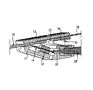
The cover 12 of the housing forms an intake 26 for the
circuit board 18. Two lateral guide slots 27 thereby guide the
insertion and withdrawal movements of the circuit board 18.
One end of a ribbon conductor 28 projects into the intake 26.
Several circuit paths 29 are arranged on the side of the
ribbon conductor 28 facing the lower section or the inserted
circuit board 18 which form end contact regions (DC contact
elements 30). These are intended to contact associated contact
regions of circuit paths 31 on the circuit board 18. When the
device is in operation, only direct currents are intended to
be transmitted via the circuit paths 29, 31, so that no
expenditure on shielding is necessary. The cover 12 of the
housing can therefore also advantageously be made of plastic
(e.g. thermoplastic). For its positioning and fixing, the
ribbon conductor 28 has positioning openings into which the
positioning posts 32 of the cover 12 project. In addition, the
ribbon conductor 28 is fixed to the cover 12 in that it is
clamped between the cover 12 and a spring element 33, with an
intervening elastomer element 34. The connection of these
elements with the cover 12 can for example be effected by
means of rivet pins 35 formed by the cover 12 which extend
through fixing openings of the spring element 33. The free
ends of the rivet pins 35 can then be deformed thermally or
through the application of pressure such that their diameter
is enlarged in the end region. This creates a form-locking
connection with the spring element 33. Preferably, the
deformation of the rivet pins 35 takes place with simultaneous
application of pressure to the spring element 33 and a
resulting compression of the elastomer element 34 which,
following deformation of the rivet pins 35, remains at least
partially erect. This leads to a largely play-free fixing of
the ribbon conductor 28 to the cover 12.
When the device is fitted, the spring element 33, formed
CA 02876631 2015-01-06
WO 2013/120580 PCT/EP2013/000214
14
as a leg spring, biases the housing or the devLce in its
closed position (first rotary position), as shown for example
in Fig. 1. In this position, the circuit board 18 cannot be
inserted into the intake 26, since the positioning posts 21
project into the intake 26.
Insertion of the circuit board 18 into the intake 26 is
only possible in the opened position of the device (second
rotary position) shown in Fig. 7. In order to open the device,
it must be pressed together manually at the end from which the
coaxial cable 19 as well as the ribbon conductor 28 emerge.
This causes the base body 11 and the cover 12 of the housing
to spread apart slightly, such that the positioning posts 21
open up the intake 26. The circuit board 18 can then be
inserted into the intake 26 until it meets an axial stop,
whereby two acutely converging notches 37 in the front edge of
the circuit board 18 interact with the positioning posts 32 of
the cover 12 in order to ensure the correct angular alignment
of the circuit board 18. Like the positioning posts 21, the
asymmetrical arrangement of the notches 37 in relation to the
longitudinal axis of the circuit board 18 prevents the circuit
board 18 from being (completely) inserted into the intake 26
the wrong side up.
Following complete insertion of the circuit board 18, the
pressure on the housing can be released. The spring element 33
then moves the two parts of the housing back into their closed
position and holds (fixes) it in this position. The
positioning posts 21 of the lower section thereby engage in
the positioning openings 22 in the circuit board 18. This
causes the circuit board 18 to be exactly positioned and fixed
in the device. At the same time, the HF contact elements 14
contact corresponding HF contact points 38 on the underside of
the circuit board 18, whereby the HF contact elements 14 are
slightly elastically deformed in order to create sufficient
CA 02876631 2015-01-06
WO 2013/120580 PCT/EP2013/000214
contact pressure and tolerance compensation. Two stop pins 36
thereby rest against the circuit board 18 and thus limit the
elastic deformation of the HF contact elements 14, preventing
them from being damaged. For this purpose, the HF contact
elements 14 project beyond the stop pins 36 by a defined
measure. The DC contact elements 30 of the ribbon conductor 28
also contact the associated circuit paths 31 on the upper side
of the circuit board 18 (DC contact pairs). The spring fingers
24 of the spring comb 23, deformed elastically through the
closure of the device, thereby ensure sufficient contact
pressure and tolerance compensation. In this exemplary
embodiment, one spring finger 24 is provided for each DC
contact pair. This makes it possible to ensure that the
necessary contact pressure is applied to each DC contact pair,
also where the circuit board 18 has a flexible carrier plate
38, and that an individual tolerance compensation is achieved
for each of these.
A corresponding functionality can also be achieved
through the use, as a substitute for the spring comb 23, of a
spring element (not shown) which possesses a common spring
base body (e.g. in the form of a leg spring), whereby
individual contact tabs made of an elastic material are
attached to the edge facing the circuit board 18 (designed as
a continuous pressure-contact edge). In this case the spring
base body can substantially ensure the contact pressure while
the contact tabs ensure individual tolerance compensation.