Note: Descriptions are shown in the official language in which they were submitted.
,
SELF-TEST GFCI DEVICE WITH
DUAL SOLENOID COIL ELECTRONIC CONTROL
CROSS-REFERENCE TO RELATED APPLICATIONS
[0001] This application contains subject matter related to subject
matter contained in
co-pending U.S. Patent Application number 13/827,785, titled, "GFCI TEST
MONITOR
CIRCUIT," by Stephen P. Simonin, U.S. Patent Application number 13/422,797,
titled,
"SOLENOID COIL HAVING AN ENHANCED MAGNETIC FIELD," by Stephen P.
Simonin, U.S. Patent Application number 13/422,790, titled, "ENHANCED AUTO-
MONITORING CIRCUIT AND METHOD FOR AN ELECTRICAL DEVICE," by
Gaetano Bonasia and Kenny Padro and U.S. Patent Application number 13/422,793,
titled, "REINSTALLABLE CIRCUIT INTERRUPTING DEVICE WITH VIBRATION
RESISTANT MIS WIRE PROTECTION," by Gaetano Bonasia et al.
,
- 1 -
CA 2876888 2021-04-06
CA 02876888 2015-01-09
Attorney Docket No. 60435
BACKGROUND
Field
[0002] The present disclosure relates generally to switched electrical
devices. More
particularly, the disclosure is directed to control circuits for circuit
interrupting devices,
such as self-testing ground fault circuit interrupter (GFCI) devices, that
switch to a
"tripped" or unlatched state from a "reset" or latched state when one or more
fault
conditions is detected. Control circuits consistent with the devices disclosed
herein have
self-testing capabilities that provide more robust end-of-life detection
capabilities than
are offered in current GFCI devices.
Description of Related Art
[0003] GFCI devices having contacts that are biased toward the open
position require
a latching mechanism for setting and holding the contacts in a closed
position. Likewise,
switched electrical devices having contacts that are biased toward the closed
position
require a latching mechanism for setting and holding the contacts in an open
position.
Examples of conventional types of devices include devices of the circuit
interrupting
type, such as circuit breakers, arc fault interrupters and GFCIs, to name a
few.
[0004] To be commercially sold in the United States a GFCI device must
conform to
standards established by the Underwriter's Laboratory (UL) in conjunction with
industry-
leading manufacturers as well as other industry members, such as various
safety groups.
One UL standard covering GFCI devices is UL-943, titled "Standard for Safety ¨
Ground
Fault Circuit Interrupters." UL-943 applies to Class A, single- and three-
phase, GFCIs
intended for protection of personnel and includes minimum requirements for the
function,
construction, performance, and markings of such GFCI devices. UL-943 requires,
among
other things, specific fault current levels and response timing requirements
at which the
GFCI device should trip. Typically, GFCIs are required to trip when a ground
fault
having a level higher than 5 milliamps (mA) is detected. Further, when a high
resistance
ground fault is applied to the device, the current version of UL-943 specifies
that the
- 2 -
CA 02876888 2015-01-09
Attorney Docket No. 60435
device should trip and prevent electrical current from being delivered to the
load in
accordance with the equation, T-420/1)143, where "T" refers to the maximum
amount of
time it can take for the device to trip and is expressed in seconds, and "I"
refers to the
minimum value of electrical current causing the fault, and is expressed in
milliamps
(mA). Thus, in the case of a 5 mA fault, the device must detect the fault and
trip, i.e.,
prevent electrical current from flowing to the load, in 7.26 seconds, or less.
[0005] With such safety-related standards in place, and because GFCI
devices are
directly credited with saving many lives since their introduction in the early
1970s, they
have become ubiquitous throughout the residential and commercial electrical
power grid,
not just in the United States, but worldwide. Like most electro-mechanical
devices,
however, GFCI devices are susceptible to failure. For example, one or more of
the
electronic components that drive the mechanical current interrupting device in
a GFCI
can short-out or otherwise become defective, as can components in the fault
detector
circuit or elsewhere within the device. Such component failures can render the
device
unable to properly detect a ground fault, and/or properly interrupt the flow
of electrical
current when a fault is detected, thus, increasing the risk of potentially
life-threatening
injury.
[0006] Because of the susceptibility for component failure, it has long
been required
that GFCI devices have a supervisory circuit that enables manual testing of
the ability of
the device to trip when a fault is encountered. Such supervisory circuits
typically include
a TEST button that, when pressed, actuates a circuit that simulates a ground
fault on the
hot and neutral conductors of the device. If the device is functioning
properly, the
simulated ground fault is detected and the device will trip, i.e., the
mechanical interrupter
is actuated. This opens the current path that connects the line side of the
device, where
the in AC power is supplied, and load side, where the user connects his or her
electrical
appliance, etc., and also where downstream receptacles or additional GFCI
devices are
connected.
[0007] A study performed several years ago by industry safety groups
indicated that
most often the public does not regularly test their GFCI devices for proper
operation, i.e.,
- 3 -
CA 02876888 2015-01-09
Attorney Docket No. 60435
by pressing the TEST button. This study further revealed that some GFCI
devices that
had been in service for an extended period of time became non-functional and
were
unable to properly detect a fault condition, thus, rendering the device
unsafe.
Specifically, it was discovered that after extended use GFCI devices fail to
trip when a
fault occurs, thus rendering the device operable as an electrical receptacle
only. That is,
the device would provide electrical power to the load contacts at all times
and not be able
to trip when a fault condition was present. Because GFCI devices were not
being
regularly tested, this unsafe condition became exacerbated. More particularly,
people
falsely believed the device was operational, in view of the fact that it was
adequately
delivering power, when in fact the device was a potentially life-threatening
hazard.
[0008] The discovery that GFCI devices deployed in the field are becoming
increasingly non-operational and unsafe in combination with the realization
that people
do not regularly test their GFCI devices, regardless of manufacturer's
explicit instructions
to do so, initiated investigations into possible changes to the UL-943
standard, including
changes that would require the GFCI devices to self-test (e.g., auto-monitor)
themselves
without the need for human intervention. The contemplated changes to UL-943
further
included a requirement for either a warning to the consumer that the device
could no
longer provide protection against a fault and/or a requirement that the device
automatically remove itself from service, e.g., permanently trip, when the
self-test failed.
Moreover, these additional self-testing operations would have to be performed
without
interfering with the primary function of the device, i.e., tripping when an
actual fault was
encountered.
[0009] The revised self-test functionality mentioned above is not yet a
requirement
for UL-943 certification, but it is expected that it will be soon. In
preparation for this
significant UL change, and in view of the seemingly endless reduction in the
cost of
integrated circuits, many GFC1 manufacturers have migrated to digital
techniques (e.g.,
microprocessors and microcontrollers) in favor of previous analog designs to
provide
both ground fault protection and self-monitoring functionality. The digital
solutions
offered thus far, however, are not ideal. For example, several related art
GFCI designs,
- 4 -
CA 02876888 2015-01-09
Attorney Docket No. 60435
including those directed at providing self-test functionality, suffer from
nuisance tripping,
a situation where the interrupter is actuated when neither a real ground
fault, a manually
generated simulated ground fault, nor an automatic self-test fault are
present. This
unfavorable condition is believed by many to be worsened by the additional
requirement
of automatic self-testing, which often results in additional inductive
currents being
generated within the device.
[0010] It is therefore desired to provide a GFCI device that provides
certain self-
testing capabilities, including those proposed in the next revision of UL-943,
but
minimizes the risks associated with nuisance tripping.
SUMMARY OF EXEMPLARY EMBODIMENTS
[0011] In consideration of problematic issues associated with related art
GFCI
devices, including but not limited to the problematic issues discussed above,
a circuit in
accordance with one or more exemplary embodiments generally relates to an auto-
monitoring circuit that continuously monitors the performance of a GFCI
device. More
specifically, a processing device, such as a microcontroller or
microprocessor, is
configured to periodically perform an auto-monitoring routine based on a
stored software
program for testing and verifying the viability and functionality of various
sub-circuits
within the GFCI device. To test proper current isolation of the GFCI device, a
driver
coupled to the microcontroller is operated to initiate a test signal
representative of a
ground fault each time the auto-monitoring routine is performed, or run, and
different
circuit nodes are monitored to confirm proper operation of the device.
[0012] A GFCI device in accordance with at least one embodiment uses a
conventional 4141 GFCI chip, or some other appropriate integrated device, to
activate a
solenoid in the presence of a trip condition, as detected by the sense and
grounded neutral
transformer coils. Similar to most conventional GFCI devices, when a trip
threshold is
detected by either of the transformer coils, a trigger signal is generated by
the 4141 chip
to activate an SCR, i.e., the trigger signal turns the SCR ON such that
current is
conducted through a solenoid coil. An aspect of a device in accordance with
this and
other embodiments utilizes dual-coils in parallel that activate the solenoid
plunger
- 5 -
CA 02876888 2015-01-09
Attorney Docket No. 60435
armature, also referred to herein as merely plunger or armature, with an
enhanced
magnetic field and, as a result, greater force is delivered to the plunger
armature than
would be delivered by a standard solenoid having a single coil.
[0013] Using two solenoid coils, however, requires additional design
considerations.
For example, it is not ideal to drive two independent SCRs with a single
trigger signal
generated by the 4141 chip because each SCR causes inherent feedback during
the time
when the 4141 chip is firing the trigger signal and driving two SCRs
simultaneously
causes a combined feedback that can damage the 4141 chip. To avoid this
potentially
damaging feedback problem a device in accordance with one or more embodiments
includes a third SCR that blocks the feedback from the two coil-driving SCRs
from
reaching the 4141 chip trigger signal output port. Thus, the design
requirements for the
4141 chip are satisfied and both coils can still be driven simultaneously.
Another
advantage of a device consistent with one or more exemplary embodiments, as
compared
to conventional GFCI devices, is that separate independent firing of the coil-
driving
SCRs can be performed. That is, according to another aspect of these
embodiments, a
gate signal from a microcontroller drives the two coil-driving SCRs under
certain
predetermined conditions while blocking the trigger signal generated by the
4141 chip
from interfering with the gate signal.
[0014] An end-of-life indicator is also coupled to the microcontroller to
indicate
whether the GFCI device has failed to properly detect the test signal or
whether some
other malfunction within the device has occurred. To avoid tripping the
mechanical
current-interrupting device when the test signal is generated, but also allow
as much of
the GFCI device circuitry to perform its intended function, a unique monitor
circuit is
provided that takes advantage of various functionality of the digital
components, such as
the GFCI integrated circuit device and the microcontroller. Specifically, to
provide an
automatic test function that monitors the fault detection capability of the
GFCI device
without interfering and causing a false trip under normal conditions,
embodiments
consistent with the invention include a specifically selected filter capacitor
associated
with the interrupter drive output of the GFCI integrated circuit (IC) device.
Proper
- 6 -
CA 02876888 2015-01-09
Attorney Docket No. 60435
selection of the capacitor and other related circuit components prevents the
interrupter
drive circuit, e.g., silicon controlled rectifier (SCR), from firing, or
turning ON, until a
real fault condition is encountered.
[0015] In accordance with one aspect of exemplary embodiments a circuit
interrupting device is provided that includes one or more line conductors for
electrically
connecting to an external power supply, one or more load conductors for
electrically
connecting to an external load, an interrupting device connected to the line
conductors
and the load conductors and electrically connecting the line conductors to the
load
conductors when the circuit interrupting device is in a reset condition and
disconnecting
the line conductors from the load conductors when the circuit interrupting
device is in a
tripped condition.
[0016] A fault detection circuit is also provided that detects a fault
condition in the
circuit interrupting device and generates a fault detection signal when the
fault condition
is detected, wherein the fault detection signal is provided to the
interrupting device to
place the circuit interrupting device in the tripped condition. An auto-
monitoring circuit
is electrically coupled to the fault detection circuit and the interrupting
device and
continuously monitors one or more signals to determine an operating state of
the circuit
interrupting device, wherein at least one of the monitored signals includes a
first auto-
monitoring input signal the value of which is at least partially determined by
a value of a
pre-trigger signal generated by the fault detection circuit, wherein the pre-
trigger signal
does not activate the interrupting device to place the circuit interrupting
device in the
tripped condition.
[0017] According to another aspect one or more exemplary embodiment, a
circuit
interrupting device is provided that includes a wiring device having a fault
detection
circuit configured to detect one or more fault conditions in the wiring device
and generate
a pre-trigger signal when the fault condition meets predetermined criteria,
wherein the
one or more fault conditions includes a self-test fault condition. A
programmable circuit
device is also provided that is programmed to execute an auto-monitoring
routine that
includes the steps of generating a self-test fault signal at a first output
port of the
- 7 -
programmable circuit device, wherein the self-test fault signal generates a
self-test fault
condition in the wiring device, input the pre-trigger signal to the
programmable circuit device at
a first input port, determining the value of the pre-trigger signal,
processing the value of the pre-
trigger signal, determining whether the fault detection circuit successfully
detected the self-test
fault based on the processed value of the pre-trigger signal, incrementing a
failure count if it is
determined that the fault detection circuit failed to successfully detect the
self-test and resetting
the failure count if it is determined that the fault detection circuit did
successfully detect the
self-test fault.
[0018] According to a further aspect of exemplary embodiments, a method of
monitoring the
operational state of an electrical wiring device is provided where the method
includes the steps
of periodically generating a self-test fault signal, detecting the self-test
fault signal, generating a
pre-trigger signal when the self-test fault signal is detected, incrementing a
counter if the value
of the pre-trigger signal is greater than or equal to a first threshold,
resetting the counter if the
value of the pre-trigger signal is less than the first threshold, determining
that either a real fault
condition or a simulated fault condition has occurred if the value of the pre-
trigger signal is
greater than a second threshold less than the first threshold, ceasing
generation of the self-test
fault signal if it is determined that either a real fault condition or a
simulated fault condition has
occurred, and continuing generation of the self-test fault signal if it is
determined that either a
real fault condition or a simulated fault condition has not occurred.
[0018A] In a broad aspect, the present invention pertains to a circuit
interrupting device
comprising one or more line conductors for electrically connecting to an
external power supply,
one or more load conductors for electrically connecting to an external load,
and a current
interrupter that disconnects the line conductors from the load conductors when
the circuit
interrupting device is in a tripped condition, and allows the line conductors
and the load
conductors to be electrically connected when said circuit interrupting device
is in a reset
condition. The current interrupter includes a solenoid with at least a first
winding that generates
a respective first magnetic force on an armature when the first winding is
electrically energized,
- 7a -
CA 2876888 2021-04-06
and a second winding that generates a respective second magnetic force on the
armature when
the second winding is electrically energized. A third magnetic force, which is
larger in
magnitude than the sum of the first and second magnetic forces, is generated
on the armature
when both the first and second windings are electrically energized at the same
time.
10081B1 In a further aspect, the present invention provides a wiring device
comprising a fault
detection circuit configured to detect one or more fault conditions in the
wiring device and to
generate a trigger signal when the fault conditions meets predetermined
criteria, and an
actuating device with coaxial first and second conductive windings, the second
conductive
winding being wound over the first conductive winding. A first switching
device is activated to
turn on when the trigger signal is received from the fault detection circuit,
and a second switch
device includes a first pin, a second pin, and a third pin, the second
switching device being
electrically connected to the first conductive winding and the first switching
device. A third
switching device includes a first pin, a second pin, and a third pin, the
third switching device
being electrically connected to the second conductive winding and the first
switching device.
Current flows through the first and second conductive windings in response to
the first
switching device being turned on.
BRIEF DESCRIPTION OF THE DRAWINGS
[0019] Exemplary embodiments of the disclosed method and device are described
in detail
below by way of example, with reference to the accompanying drawings, in
which:
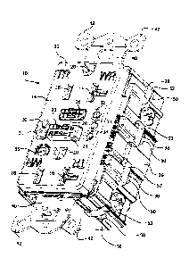
[0020] FIG. 1 is a side elevation view of a self-testing GFCI receptable
device in accordance
with an exemplary embodiment;
[0021] FIG. 2 is a side elevation view of the self-testing GFCI receptacle
shown in FIG. 1
with the front cover of the housing removed;
[0022] FIG. 3 is a side elevation view of a core assembly of the self-testing
GFCI receptacle
device shown in FIG. 1;
- 8 -
CA 2876888 2021-04-06
[0023] FIGS. 4A-4D is a schematic of an exemplary circuit consistent
with an
exemplary embodiment;
[0024] FIG. 5 is an elevation view of a dual-coil solenoid used in
connection with a
GFCI receptacle in accordance with an exemplary embodiment;
[0025] FIG. 6 is sectional (cutaway) view of the dual-coil solenoid of
FIG. 5 with
bobbin and plunger shown.
DETAILED DESCRIPTION OF EXEMPLARY EMBODIMENTS
[0026] Exemplary embodiments include one or more of the novel
mechanical and/or
electrical features described in detail below. For example, one or more of the
exemplary
embodiments disclosed include auto-monitoring or, self-test, features. Some
self-test
features and capabilities with respect to GFCI devices have been disclosed
previously, for
example, in U.S. patent nos. 6,807,035, 6,807,036, 7,315,437, 7,443,309 and
7,791,848,
and U.S. patent publication number 2013/0242440 Al, September 19, 2013, all of
- which are commonly assigned to the same assignee as this application and
which may
be reviewed for further details. An auto-monitoring feature consistent with
the method
and devices disclosed herein is more robust than that which has been
previously
disclosed and reduces the probability of false or nuisance tripping by the
device. For
example, additional features are provided that relate to the determination of
an end-of-
life (EOL) condition and actions taken subsequent to such determination.
Further
exemplary novel electrical and mechanical features are described herein below
with
reference to the figures.
[0027] Referring to FIG. 1, a GFCI receptacle 10 according to an
exemplary
embodiment includes a front cover 12 having a duplex outlet face 14 with phase
16,
neutral 18 and ground 20 openings. Face 14 also has opening 22 accommodating
RESET
button 24 adjacent to opening 26 accommodating TEST button 28, and six
respective
circular openings, 30-35. In accordance with this exemplary embodiment
openings 30,
33 accommodate two respective indicators, such as different colored LEDs,
openings 32,
34 accommodate respective bright LEDs used, for example, as a nightlight,
opening 31
accommodates a photoconductive photocell used, for example, to control the
nightlight
- 9 -
CA 2876888 2021-04-06
LEDs, and opening 35 provides access to a set screw for adjusting a photocell
device in
accordance with this and other exemplary embodiments. Rear cover 36 is secured
to
front cover 12 by eight fasteners 38 ¨ four of the eight fasteners 38 are
shown in FIG. 1
and the four additional fasteners 38 are provided on the side of receptacle 10
obscured
from view in FIG. 1. For example, each fastener 38 may include a barbed post
50 on
front cover 12 and corresponding resilient hoop 52 on rear cover 36, similar
to that which
is described in detail in U.S. patent number 6,398,594, the entire contents of
which may
be reviewed for further details. Ground yoke/bridge assembly 40 having
standard
mounting ears 42 protrudes from the ends of receptacle 10.
[0028] Referring to FIG. 2, front cover 12 of GFCI receptacle 10 has
been removed
to expose manifold 126, which provides support for printed circuit board 390
and
yoke/bridge assembly 40. According to the embodiment shown, manifold 126
includes
four dovetail interconnects 130 that mate with corresponding cavities 132
along the upper
edge of rear cover 36. One dovetail-cavity pair is provided on each of the
four sides of
manifold 126 and rear cover 36, respectively.
[0029] FIG. 3 is a side elevation view of core assembly 80. Core
assembly 80
includes circuit board 82 that supports most of the working components of the
receptacle
device, including the circuit shown in FIGS. 4A-4D, sense transformer 84 and
grounded
neutral transformer 85 (not shown). Line contact arms 94, 96 pass through
transformers
84, 85 with an insulating separator 98 therebetween. Line contact arms 94, 96
are
cantilevered, their respective distal ends carrying phase and neutral line
contacts 102,
104. Load contact arms 98, 100 are also cantilevered with their respective
distal ends
carrying phase and neutral load contacts 101, 103. The resiliency of the
cantilevered
contact arms biases the line contacts 102, 104 and load contacts 101, 103 away
from
eachother, thus keeping the contacts electrically isolated from eachother
under normal
conditions. At or near their respective distal ends, load contact arms 98, 100
rest on a
movable contact carriage 106, made of insulating (preferably thermoplastic)
material.
[0030] FIGS. 4A-4D, hereafter collectively referred to as FIG. 4, is a
schematic
drawing of the electro-mechanical components of a GFCI receptacle device
consistent
- 10 -
CA 2876888 2021-04-06
CA 02876888 2015-01-09
Attorney Docket No. 60435
with one or more of the exemplary embodiments. According to these embodiments,
the
circuit shown in FIG. 4 is employed in a GFCI device as described above. The
circuit of
FIG. 4 is consistent with the mechanical operation of the exemplary
embodiments
described above; however, a GFCI device consistent with these embodiments need
not
employ the precise electrical circuit depicted in FIG. 4 and those of ordinary
skill in the
art, after viewing FIG. 4 and/or reviewing the description set forth below,
would be able
to modify certain aspects of the circuit to achieve similar overall results.
Such
modifications are contemplated and believed to be within the scope of the
invention set
forth herein.
[0031] The circuit shown in FIG. 4, or various sub-circuits thereof, can be
implemented in a variety of electrical wiring devices. For purposes of
description here,
however, the circuit of FIG. 4 is discussed in conjunction with its use in the
GFCI
receptacle device shown in FIGS. 1-3.
[0032] The circuit shown in FIG. 4 includes phase line terminal 326 and
neutral line
terminal 328 for electrical connection to an AC power source (not shown), such
as a 60-
hertz, 120 Volt RMS power source used in the United States for mains power in
connection with both residential and commercial applications. The circuit of
FIG. 4 and
software resident within one or more components of the circuit can be modified
to
accommodate other power delivery systems as well. Such modifications and the
resultant
circuit and wiring devices in which the circuit and software would be
implemented are
contemplated by the inventor and considered to be within the spirit and scope
of the
invention described herein. For example, power delivery systems that use
different
voltages and frequencies are within the scope of the invention.
[0033] Referring to FIG. 4, phase conductor 330 and neutral conductor 332
are
respectively connected to the phase and neutral line terminals and each passes
through
sense transformer 334 and grounded neutral transformer 336, both of which are
part of a
detection circuit described below. By way of example, phase and neutral line
terminals
correspond to input terminal screws 326, 328 in FIG. 1 and phase and neutral
line
conductors 330, 332 represent line contact arms 94, 96, respectively, as
described above
- 11 -
CA 02876888 2015-01-09
Attorney Docket No. 60435
with respect to FIG. 3. Each of line conductors 330, 332 has a respective
fixed end
connected to the phase and neutral line terminals and each includes a
respective movable
contact, e.g., contacts 102, 104 from the embodiment described above. Face
phase and
face neutral conductors 338, 340, respectively, include electrical contacts
(not shown)
fixed thereto. The face conductors are electrically connected to and, in the
embodiment
shown, are integral with, respective face terminals 342, 344, to which plug
blades from a
load device (not shown), such as an electrical appliance, would be
electrically connected
when the electrical receptacle device is in use.
[0034] The circuit shown in FIG. 4 according to this embodiment also
includes
optional load phase and load neutral terminals 346, 348, respectively, which
electrically
connect to a downstream load (not shown), such as one or more additional
receptacle
devices. Load terminals 346, 348 are respectively connected to cantilevered
load
conductors 227, 228, each of which includes a movable contact (not shown in
FIG. 4) at
its distal end. The load contacts are disposed below respective phase and
neutral line
contacts and phase and neutral face contacts and are coaxial with them such
that when the
line conductors are moved toward the load and face conductors, the three sets
of contacts
mate and are electrically connected together. When the device is in this
condition it is
said to be "reset" or in the reset state.
THE DETECTOR CIRCUIT
[0035] With continued reference to FIG. 4, detector circuit 352 includes
transformers
334, 336 as well as a GFCI integrated circuit device (GFCI IC), 350. In
accordance with
the present embodiment GFCI IC 350 is the well-known 4141 device, such as an
RV4141
device made by Fairchild Semiconductor Corporation. Other GFCI IC devices
could
potentially be used in the circuit of FIG. 4 instead of the 4141 device and
such a
modification is within the spirit and scope of the method and devices
disclosed herein.
[0036] GFCI IC device 350 receives electrical signals from various other
circuit
components, including transformers 334, 336, and detects one or more types of
faults,
such as a real ground fault, a simulated ground fault or a self-test ground
fault, as well as
- 12 -
CA 02876888 2015-01-09
Attorney Docket No. 60435
a real or simulated grounded neutral fault. For example, when a sufficient
current
imbalance between line conductors 330, 332 occurs, a net current flows through
the
transformers 334, 336, causing a magnetic flux to be created about at least
transformer
334. This magnetic flux results in electrical current being induced on
conductor 333,
which is wound around sense transformer 334. Respective ends of conductor 333
are
connected to the positive and negative inputs to the sense amplifier of GFCI
IC device
350 at input ports V-REF and VFB, respectively. The induced current on
conductor 333
causes a voltage difference at the inputs to the sense amplifier of GFCI IC
350. When the
voltage difference at the inputs to the sense amplifier of GFCI IC 350 exceeds
a
predetermined threshold value, a detection signal is generated at one or more
output ports
of GFCI IC 350, such as the SCR trigger signal output port (SCR_OUT). The
threshold
value used by GFCI IC 350 is determined by the effective resistance connected
between
the op-amp output (OP_OUT) and the positive input to the sense amplifier
(VFB).
[0037] The current imbalance on line conductors 330, 332 typically results
from
either a real ground fault, a simulated ground fault or a self-test ground
fault. A
simulated ground fault is generated when test switch 354 (FIG. 4B) closes,
which occurs
when TEST button 28 (FIG. 1) is pressed by the user. As described in further
detail
below, a self-test fault occurs when auto-monitoring circuit 370 (FIG. 4D)
initiates an
auto-monitoring test sequence that includes an electrical current being
generated on
independent conductor 356 (FIG. 4A).
[0038] According to the present embodiment, when test switch 354 closes,
some of
the current flowing in line conductors 330, 332 and load conductors 338, 340
is diverted
from the phase face conductor 338 (and phase load conductor 277 when the
device is in
the reset state) around sense transformer 334 and through resistor 358 to
neutral line
conductor 332. By diverting some of the current through resistor 358 in this
manner, an
imbalance is created in the current flowing through conductor 330 and the
current
flowing in the opposite direction through conductor 332. When the current
imbalance,
i.e., the net current flowing through the conductors passing through the sense
transformer,
exceeds a threshold value, for instance 4-5 milliamps, this simulated ground
fault is
- 13 -
CA 02876888 2015-01-09
Attorney Docket No. 60435
detected by detector circuit 352 and the SCR drive output of GFCI IC 350
(SCR_OUT) is
activated.
[0039] When the SCR drive output of GFCI IC 350 is activated, the gate of
SCR3
360 is turned ON allowing current to flow from the phase line conductor 330
through
diode 359, a resistor network R15, R3, R19, and SCR3 360. The current flowing
through
SCR3 360 generates a voltage at, and turns ON, the gates of SCR1 361 and SCR2
369.
When SCR1 361 is turned ON, current flows from phase line conductor 330
through
secondary coil 363 of dual-coil solenoid 362, fuse 365, diode 367 and SCR1
361.
Further, when SCR2 369 is turned ON, current flows from phase line conductor
330
through primary coil 364 of dual-coil solenoid 362, fuse 372, diode 374 and
SCR2 369.
The current flowing through each of coils 363, 364 generates a magnetic field
that moves
an armature within solenoid 362.
[0040] When the solenoid armature moves, it unlatches a contact carriage,
(e.g., 106
in FIG. 3) which is part of interrupting device 315, and the carriage drops
under the
natural bias of line conductors 330, 332, that is, away from the face
conductors 338, 340
and load conductors 277, 278. The device is now said to be "tripped," as a
result of the
successful manually generated simulated fault test sequence, and the device
will not
deliver power to a load until it is reset, i.e., by pressing the RESET button.
The time it
takes from the instant switch 354 closes until the device is tripped and
current no longer
flows from phase line conductor 330 to either the face and load conductors and
through
solenoid coils 363, 364, is so short that fuses 365, 372 remain intact.
[0041] According to the present embodiment, GFCI IC 350 is a conventional
4141
chip. Similar to most conventional GFCI devices, when a trip threshold is
detected by
either of the transformer coils, 334, 336, a trigger signal is generated by
the 4141 chip to
activate an SCR, i.e., the trigger signal turns the SCR ON such that it
conducts current
through a solenoid coil. An aspect of a device in accordance with this and
other
embodiments utilizes dual coils in parallel that activate the solenoid plunger
with an
enhanced magnetic field and, as a result, greater force is delivered to the
plunger than
would be delivered by a standard solenoid having a single coil.
- 14 -
CA 02876888 2015-01-09
Attorney Docket No. 60435
[0042] Referring to FIGS. 5 and 6, a dual-coil solenoid according to at
least one
exemplary embodiment includes a bobbin 1100 with a hollow center and a metal
armature, or plunger 1105, therein. The solenoid 600, shown in FIG. 5 without
a bobbin,
illustrates the beginning and ending of the respective coils or windings. As
shown,
solenoid 600 includes a primary winding 602 that has a starting end and a
terminating
end distal from the starting end. Primary winding 602 imparts a first magnetic
force
when the primary winding is electrically energized. Solenoid 600 also includes
a
secondary winding 604 with a starting end and a terminating end distal from
the starting
end that is wound on top of the primary winding 602. Secondary winding 604
imparts a
second magnetic force when the secondary winding is electrically energized.
When the
primary and secondary windings are energized simultaneously, a third magnetic
force is
imparted on the plunger.
[0043] The third magnetic force which is generated when both the first and
second
coils are energized simultaneously is significantly greater than the
combination of the
first and second magnetic forces. For example, referring to FIG. 6, a dual-
coil solenoid is
wound on bobbin 1100 in accordance with at least one embodiment. Secondary
winding
1104 comprising 950 turns of 33 AWG wire is wound directly on top of primary
winding
1102 which comprises 800 turns of 35 AWG wire. As shown, both windings are
wound
on bobbin 1100 which includes cylindrical plunger 1105 disposed within a
hollow cavity
of the bobbin.
[0044] When a solenoid consistent with the one described above was tested,
a
combined magnetic force of 5.5 lbs. was generated. Specifically, when only the
primary
winding 1102 was energized it produced 2.5 lbs. of force on plunger 1105 and
when only
the secondary winding 1104 was energized; it produced 1.4 lbs. of force on the
plunger
1105. However, when both the primary and the secondary windings were energized
together, i.e., at the same time, a total of 5.5 lbs. of force was imparted on
plunger 1105,
which is an approximate 42% improvement in delivered force over the mere
combination, i.e., sum, of the two independent forces. As a result, it is
possible to drive
the plunger/armature with greater force than is otherwise available when a
single winding
- 15 -
solenoid is employed or when a redundant coil design is employed and only one
or the
other winding is energized at any given time. Increasing the delivered
magnetic force on
the plunger provides advantages such as a higher probability of opening the
contacts
when, for example, the contacts have welded together. Further details of
solenoid 600
and other various configurations thereof, consistent with the present
invention, can be
found in co-pending U.S. patent publication No 2013/0241675 Al, September 19,
2013,
which may be reviewed for any further details.
[0045] In regard to the above embodiment, it has further been observed
that an even
stronger combined magnetic force can be achieved on plunger 1105 under certain
operating conditions; for example, magnetic forces of up to 12 lbs. have been
observed.
For example, as discussed in several other places within this disclosure,
during normal
operation of a GFCI device the solenoid is activated by the GFCI IC device 350
(FIG. 4)
to drive the plunger such that the interrupter mechanically trips, thus
separating the
electrical contacts of the device. If a failure occurs within the device,
however, such as
SCR3 creating an open-circuit, the GFCI IC device 350 will be unable to
activate the
solenoid, for example, by driving the gate of SCR3.
[0046] According to the present embodiment, as well as others,
programmable device
301 detects this condition and independently drives the respective SCRs, e.g.,
SCR1 and
SCR2 in FIG. 4. If the device does not trip the first time programmable device
301
drives the SCRs, the plunger in the solenoid is biased, e.g., by a spring or
some other
force, back to its original, static, position within the solenoid. Due to the
timing of the
drive signal provided by programmable device 301, as controlled by its
resident software,
a subsequent drive signal is provided at the precise time the plunger is being
biased in
this reverse direction, and is in motion in a direction opposite the magnetic
force of the
solenoid. As a result, a magnetic force much greater than when the plunger is
actuated
from its static position is imparted on the plunger. For example, as
mentioned, a
magnetic force of approximately 12 lbs. has been measured under these
conditions.
Although this condition is a failure condition and would not occur when the
device is
operating normally, it provides a situation where the contacts are driven with
an even
- 16 -
CA 2876888 2021-04-06
CA 02876888 2015-01-09
Attorney Docket No. 60435
stronger force to open, e.g., in the event the contacts are welded or
otherwise unable to
separate. According to this embodiment, the programmable device 350 detects
this
situation as an end-of-life (EOL) condition and activates one or more of an
audio and
visual indication, for example, by activating PCB 390 in FIG. 4.
[0047] Using two parallel solenoid coils in the GFCI detection circuit as
discussed
above, however, requires additional design considerations. For example, it is
not ideal to
drive two independent SCRs with a single trigger signal generated by the 4141
chip.
Specifically, each SCR causes inherent feedback during the time when the 4141
chip is
firing the trigger signal. Thus, driving two SCR devices simultaneously causes
a
combined feedback that can possibly damage the 4141 chip. Referring again to
FIG. 4, to
avoid this potentially damaging feedback problem a GFCI device in accordance
with
embodiments of the present invention includes a third SCR, e.g., SCR3 360 in
the
embodiment described above. The third SCR blocks the feedback from the two
coil-
driving SCRs, e.g., SCR1 361 and SCR2 369 in the above embodiment, from
reaching
the 4141 chip trigger signal output port, e.g., SCR_OUT.
[0048] Thus, by including the third SCR between the GFCI IC device and the
coil-
driving SCRs, the design requirements for the GFCI IC device are satisfied and
both coils
can be driven simultaneously. Another advantage of a device consistent with
exemplary
embodiments, as compared to conventional GFCI devices, is that separate
independent
firing of the coil-driving SCRs can be performed. In particular, a gate signal
from a
microcontroller drives the two coil-driving SCRs under certain predetermined
conditions
while blocking the trigger signal generated by the 4141 chip from interfering
with the
gate signal. 110 port GP2 of programmable device 301 can be programmed to
activate
the respective gates of SCR' 361 and SCR2 369. When these two SCRs fire and
conduct
electrical current, the third SCR, i.e., SCR3 360 blocks any feedback from
SCR1 361 and
SCR2 369 from damaging the SCR drive port (SCR_OUT) of GFCI IC device 350.
- 17 -
CA 02876888 2015-01-09
Attorney Docket No. 60435
MANUAL TESTING VIA THE RESET OPERATION
[0049] Referring to FIG. 4, closing reset switch 300, e.g., by pressing
RESET button
24 (FIG. 1), also initiates a test operation. Specifically, when reset switch
300 closes, a
voltage supply output, VS, of GFCI IC 350 is electrically connected to the
gate of SCR
360 through conductor 308, thus, turning ON SCR 360. When SCR 360 is turned
ON,
current is drawn from line conductor 330 through diode 359 and SCR 360 and
ultimately
to ground. Similar to when SCR 360 is turned ON by pressing the TEST button,
as
discussed previously, turning ON SCR 360 by pressing the RESET button results
in SCR
361 and SCR 369 also being turned ON and current flowing through solenoid
coils 363,
364. The current flowing through coils 363, 364 of solenoid 362 generates a
magnetic
field at the solenoid and the armature within the solenoid is actuated and
moves. Under
typical, e.g., non-test, conditions, the armature is actuated in this manner
to trip the
device, such as when an actual fault occurs.
[0050] When reset switch 300 closes, however, the device is likely already
in the
tripped condition, i.e., the contacts of the line, face and load conductors
are electrically
isolated. That is, the RESET button is usually pressed to re-latch the contact
carriage and
bring the line, face and load contacts back into electrical contact after the
device has
tripped. If the armature of solenoid 362 fails to fire, i.e., move, when the
RESET button
is pressed, and the reset mechanism, including the contact carriage, fails to
engage the
reset plunger on its return after the RESET button is released, the device
will not reset.
Accordingly, if, for example, the device has not been wired to the AC power
lines, or it
has been mis-wired, that is, the device has been wired with the AC power not
connected
to the line terminals, 326, 328, no power is applied to the GFCI IC 350. If no
power is
applied to GFCI IC 350, the gate of SCR 360 cannot be driven, either by the
SCR output
of GFCI IC 350 or when the RESET button is pressed. Under this condition the
device
will not be able to be reset. The mis-wire condition is prevented in
accordance with a
wiring device consistent with the present embodiment by ensuring the device is
shipped
- 18 -
CA 02876888 2015-01-09
Attorney Docket No. 60435
to the user in the tripped condition. Because the device cannot be reset until
AC power is
properly applied to the line terminals, the mis-wire condition is prevented.
THE AUTO-MONITORING CIRCUIT
[0051] With continued reference to the exemplary circuit schematic shown in
FIG. 4,
auto-monitoring circuit 370 includes a programmable device 301. Programmable
device
301 can be any suitable programmable device, such as a microprocessor or a
microcontroller, which can be programmed to implement the auto-monitoring
routine as
explained in detail below. For example, according to the embodiment shown in
FIG. 4,
programmable device 301 is implemented by an ATMELTm microcontroller from the
ATtiny 10 family. It could also be implemented by a Microchip microcontroller
such as
a PIC10F204/206.
[0052] According to one exemplary auto-monitoring, or automatic self-
testing,
routine in accordance with the embodiment shown in FIG. 4, microcontroller 301
initiates
the auto-monitoring routine approximately every three (3) seconds by setting a
software
auto-monitoring test flag. The auto-monitoring test flag initiates the auto-
monitoring
routine within the circuit interrupting device and confirms that the device is
operating
properly or, under certain circumstances, determines that the circuit
interrupting device
has reached its end-of-life (EOL). When the auto-monitoring routine runs with
a
positive, i.e., successful, result, the auto-monitoring circuit enters a
hibernation state until
microcontroller 301 sets the test flag again and initiates another auto-
monitoring routine.
[0053] If the auto-monitoring routine runs with a negative result, e.g., it
cannot be
determined that the circuit interrupting device is functioning properly or it
determines
that it is, in fact, not operating properly, a failure counter is incremented
and
microcontroller 301 initiates another auto-monitoring routine when instructed
by the
software program stored in memory within the device. In addition to the
failure count
being incremented, a temporary indication of the failure is also provided. For
example,
according to the present embodiment, when such a failure occurs, I/O port GPO
of
microcontroller 301 is controlled to be an output and light emitting diode
(LED) 376 is
- 19 -
CA 02876888 2015-01-09
or
Attorney Docket No. 60435
controlled to flash, e.g., one or more times, to indicate the failure to a
user. If the failure
counter reaches a predetermined value, i.e., the auto-monitoring routine runs
with a
negative result a certain number of times, the number being stored and
implemented in
software, the auto-monitoring routine invokes an end-of-life (EOL) sequence.
The EOL
sequence includes one or more of the following functions; (a) indicate that
EOL has been
reached, for example, by continuously flashing or illuminating an indicator
light and/or
generating an audible sound, (b) attempt to trip the device, (c) prevent an
attempt to reset
the device, (d) store the EOL event on non-volatile memory, e.g., in the event
there is a
power failure, and (e) clear the EOL condition when the device is powered
down.
[0054] In accordance with this embodiment, when the auto-
monitoring software
determines it is time to run the auto-monitoring routine, i.e., based on the
auto-monitor
timer, a stimulus signal 302 is turned ON at I/O port GPI of microcontroller
301. When
the stimulus signal is turned ON, electrical current flows through resistor
303 and a
voltage is established at the base of transistor 304, turning the transistor
ON. When
transistor 304 is turned ON, current flows from dc voltage supply 378 through
resistor
305, which is, for example, a 3k-ohm resistor, and continues through
electrical conductor
356 and transistor 304 to ground. Regarding dc voltage source 378, according
to the
present embodiment the value of this voltage source is designed to be between
4.1 and
4.5 volts dc, but the value of this voltage supply can be any other suitable
value as long as
the value used is adequately taken into account for other circuit
functionality described
below.
[0055] According to this exemplary embodiment, electrical
conductor 356 is a wire,
but it could also be a conductive trace on a printed circuit board. Conductor
356 is
connected at one end to resistor 305, traverses through sense transformer 334
and is
looped approximately ten (10) times around the core of the transformer and
connected at
its other end to the collector of transistor 304. Thus, when the software auto-
monitoring
test flag is set in microcontroller 301 and transistor 304 is turned ON,
current flows
through conductor 356 which comprises an independent conductor separate from
phase
- 20 -
CA 02876888 2015-01-09
Attorney Docket No. 60435
line conductor 330 and neutral line conductor 332, which also traverse through
the center
of sense transformer 334.
[0056] If the circuit interrupting device according to the present
embodiment is
functioning properly, as current flows through conductor 356 and through the
sense
transformer a magnetic flux is generated at sense transformer 334. The flux
generates a
signal on conductor 333 which is detected by detection circuit 352, including
GFCI IC
device 350. In accordance with this embodiment, when device 350 detects the
flux
created at sense transformer 334, a voltage level is increased at one of the
I/0 ports of
device 350, for example at the output port labeled CAP in FIG. 4, thus
increasing the
voltage on conductor 306.
[0057] According to this embodiment, capacitor 307 is connected between the
CAP
I/0 port of microcontroller 301 and ground. As is known in the art, attaching
a capacitor
directly between the CAP output of a 4141 GFCI IC device and ground causes the
SCR
trigger signal (SCR_OUT) output from GFCI IC device 350 to be delayed by a
predetermined period of time. The amount of time the trigger signal is delayed
is
typically determined by the value of the capacitor. According to the present
embodiment,
however, capacitor 307 is not connected directly between the CAP output and
ground.
Instead, capacitor 307 is also connected to the ADC I/0 port GPO of
microcontroller 301
via a circuit path that includes diode 310 in series with resistor 311, e.g.,
3 M-Ohm,
which completes a voltage divider circuit with resistor 312, e.g., 1.5 M-Ohm.
This
additional circuitry connected to the capacitor at the CAP output of GFCI IC
device 350
drains current from the delay capacitor.
[0058] By measuring the value of the signal at ADC 1/0 port (GPO) and
confirming it
is above a certain level, it can be determined whether or not the self-test
fault signal
generated on conductor 356 was properly detected by detection circuit 352 and
it can
further be confirmed whether GFCI IC device 350 is capable of generating the
appropriate SCR trigger signal. Also, to avoid tripping the device during a
self-test auto-
monitoring fault, the voltage at capacitor 307 is measured and proper self-
test fault
- 21 -
CA 02876888 2015-01-09
Attorney Docket No. 60435
detection is confirmed before a drive signal is output at SCR_OUT of GFCI IC
device
350.
[0059] If the current drain on capacitor 307 is too high, GFCI IC device
350 may not
operate properly. For example, if as little as 3-4 microamps ( A) of current
is drained
from capacitor 307, grounded neutral conditions, which are also intended to be
detected
by GFCI IC device 350, may not be accurately detected, e.g., pursuant to UL
requirements, because the SCR trigger signal (SCR_OUT) will not fire within
the
necessary amount of time. According to the present embodiment, less than about
1.3
microamps, or about 5% of the specified delay current for the GFCI IC device
350, is
drained for the ADC I/0 port GPO of microcontroller 301. This small current
drain from
capacitor 307 has no effect on the ability of the device to properly detect
real ground
faults and/or real grounded neutral faults.
[0060] According to this embodiment, approximately 50 nanoamps (nA) of
current is
drawn off of capacitor 307. Parallel resistors 311 and 312 connected to the
ADC I/0 port
GPO of microcontroller 301 create a 4.5 megaohm (Me) drain which limits the
current
pulled from capacitor 307 to a maximum of 1.0 microamp. GFCI IC device 350
uses
approximately 40 microamps of current to generate the SCR trigger but
microcontroller
301 only requires approximately 50 nanoamps to read the SCR trigger signal off
of
capacitor 307 before the SCR trigger signal is output from SCR_OUT.
Accordingly, by
selecting the proper value for capacitor 307, in conjunction with appropriate
value
selections for resistors 311 and 312, as well as diode 310, it is possible to
maintain the
correct delay for the SCR trigger signal (SCR_OUT) from GFCI IC device 350 and
use
the ADC in microcontroller 301 to measure the signal at ADC input (GPO) to
determine
whether the test signal on conductor 356 has been properly detected by
detection circuit
352.
[0061] It should also be noted that in the embodiment shown in FIG. 4, LED
376 is
also connected to ADC I/0 port (GPO) of microcontroller 301. Accordingly,
whether or
not LED 376 is conducting or not will affect the drain on capacitor 307, as
well as the
delay of the SCR trigger signal and the ability of microcontroller 301 to
properly measure
- 22 -
CA 02876888 2015-01-09
Attorney Docket No. 60435
the signal output from the CAP I/0 port of GFCI IC device 350. Thus, in regard
to the
circuit shown in FIG. 4, I FD 376 is selected such that it does not turn ON
and begin
conducting during the time microcontroller 301 is measuring the signal from
the CAP
output of GFCI IC device 350. For example, LED 376 is selected such that its
turn-ON
voltage is about 1.64 volts, or higher which, according to the circuit shown
in FIG. 4, can
be measured at I/0 port GPO. Additionally, to prevent any signal adding to
capacitor 307
when LED 376 is being driven, diode 310 is provided.
[0062] According to this embodiment, the circuit path that includes diode
310 and the
voltage divider, 311, 312, is connected to I/0 port GPO of microcontroller
301, which
serves as an input to an analog-to-digital converter (ADC) within
microcontroller 301.
The ADC of microcontroller 301 measures the increasing voltage established by
the
charging action of capacitor 307. When a predetermined voltage level is
reached,
microcontroller 301 turns OFF the auto-monitoring stimulus signal 302 which,
in turn,
turns OFF transistor 304, stopping the current flow on conductor 356 and,
thus, the flux
created at sense transformer 334. When this occurs, it is determined by
microcontroller
301 that a qualified auto-monitoring event has successfully passed and the
auto-
monitoring fail counter is decremented if the present count is greater than
zero.
[0063] In other words, according to this embodiment an auto-monitoring
routine is
repeated by microcontroller 301 on a predetermined schedule. Based on the
software
program stored in memory within microcontroller 301, the auto-monitoring
routine is
run, as desired, anywhere from every few seconds to every month, etc. When the
routine
is initiated, the flux created at sense transformer 334 occurs in similar
fashion to the
manner in which flux would be created if either an actual ground fault had
occurred or if
a simulated ground fault had been manually generated, e.g., by pressing the
TEST button
as described above.
[0064] There is a difference, however, between an auto-monitoring (self-
test) fault
generated by the auto-monitoring routine and either an actual ground fault or
a simulated
fault generated by pressing the TEST button. When either an actual or
simulated ground
fault occurs, a difference in the current flowing in the phase and neutral
conductors, 330
- 23 -
CA 02876888 2015-01-09
Attorney Docket No. 60435
and 332, respectively, should be generated. That is, the current on conductor
330 should
be different than the current on conductor 332. This differential current
flowing through
sense transformer 334 is detected by GFCI IC device 350, which drives a signal
on its
SCR_OUT I/0 port to activate the gate of SCR 360 and turn it ON. When SCR 360
turns
ON, current is drawn through coils 363, 364 which causes interrupting device
315 to trip,
causing the contact carriage to drop which, in turn, causes the line, face and
load contacts
to separate from each other. Thus, current is prevented from flowing through
phase and
neutral conductors 330, 332 to the phase and neutral face terminals 342, 344,
and the
phase and neutral load terminals 346, 348, respectively.
[0065] In comparison, when the auto-monitoring routine is performed in
accordance
with the present invention, no differential current is created on the phase
and neutral
conductors 330, 332 and the interrupting device 315 is not tripped. Instead,
during the
auto-monitoring routine, the flux generated at sense transformer 334 is a
result of current
flowing through conductor 356, which is electrically separated from phase and
neutral
conductors 330, 332. The current generated on conductor 356 is present for
only a brief
period of time, for example, less than the delay time established by capacitor
307,
discussed previously.
[0066] If the voltage established at the input to the ADC input (GPO) of
microcontroller 301 reaches a programmed threshold value within this
predetermined
period of time during an auto-monitoring routine, it is determined that the
detection
circuit 352 successfully detected the current flowing through the core of
sense
transformer 334 and the auto-monitoring event is deemed to have passed.
Microcontroller 301, thus, determines that detection circuit 352, including
GFCI IC
device 350, is working properly. Because the current flowing through sense
transformer
334 during the auto-monitoring routine is designed to be substantially similar
in
magnitude to the differential current flowing through the transformer during a
simulated
ground fault, e.g., 4-6 milliamps, it is determined that detection circuit 352
would be able
to detect an actual ground fault and provide the proper drive signal to SCR
360 to trip
interrupter 315.
- 24 -
CA 02876888 2015-01-09
Attorney Docket No. 60435
[0067] Alternatively, auto-monitoring circuit 370 might determine that the
auto-
monitoring routine failed. For example, if it takes longer than the
predetermined period
of time for the voltage at the ADC input at GPO of microcontroller 301 to
reach the given
voltage during the auto-monitoring routine, it is determined that the auto-
monitoring
event failed. If this occurs, an auto-monitoring fail tally is incremented and
the failure is
indicated either visually or audibly. According to one embodiment, the ADC
port (GPO)
of microcontroller 301 is converted to an output port when an auto-monitoring
event
failure occurs and a voltage is placed on conductor 309 via I/0 port GPO,
which is first
converted to a output port by the microcontroller. This voltage at GPO
generates a
current on conductor 309 that flows through indicator LED 376 and resistor 380
to
ground. Subsequently, ADC I/0 port (GPO) of microcontroller 301 is converted
back to
an input port and remains ready for the next scheduled auto-monitoring event
to occur.
[0068] According to this embodiment, when an auto-monitoring event failure
occurs,
indicator LED 376 illuminates only for the period of time when the I/0 port is
converted
to an output and an output voltage is generated at that port; otherwise LED
376 remains
dark, or non-illuminated. Thus, if the auto-monitoring routine is run, for
example, every
three (3) seconds, and an event failure occurs only a single time or
sporadically, the event
is likely to go unnoticed by the user. If, on the other hand, the failure
occurs regularly, as
would be the case if one or more of the components used in the auto-monitoring
routine
is permanently disabled, indicator LED 376 is repetitively turned ON for 10
msec and
OFF for 100 msec by microcontroller 301, thus drawing attention to the device
and
informing the user that critical functionality of the device has been
compromised.
Conditions that cause the auto-monitoring routine to fail include one or more
of the
following, open circuited differential transformer, closed circuited
differential
transformer, no power to the GFCI IC, open circuited solenoid, SCR trigger
output of the
GFCI IC continuously high, and SCR output of the GFCI IC continuously low.
[0069] According to a further embodiment, if the auto-monitoring fail tally
reaches a
predetermined limit, for example, seven (7) failures within one (1) minute,
microcontroller 301 determines that the device is no longer safe and has
reached its end-
- 25 -
CA 02876888 2015-01-09
,
Attorney Docket No. 60435
of-life (EOL). If this occurs, a visual indicator is activated to alert the
user that the circuit
interrupting device has reached the end of its useful life. For example, when
this EOL
state is determined, the ADC 1/0 port (GPO) of microcontroller 301 is
converted to an
output port, similar to when a single failure is recorded as described above,
and a signal is
either periodically placed on conductor 309 via GPO, i.e., to blink LED 376 at
a rate of,
for example, 10 msec ON and 100 msec OFF, or a signal is continuously placed
on
conductor 309 to permanently illuminate LED 376. The auto-monitoring routine
is also
halted at this time.
[0070] In addition to the blinking or continuously illuminated
LED 376, according to
a further embodiment when EOL is determined, an optional audible alarm circuit
382 on
printed circuit board (PCB) 390 is also activated. In this situation the
current through
LED 376 establishes a voltage on the gate of SCR 384 such that SCR 384 is
turned ON,
either continuously or intermittently, in accordance with the output signal
from GPO of
microcontroller 301. When SCR 384 is ON, current is drawn from phase line
conductor
330 to activate audible alarm 386 (e.g., a buzzer) providing additional notice
to a user of
the device that the device has reached the end of its useful life, i.e., EOL.
For example,
with respect to the present embodiment, audible alarm circuit 382 includes a
parallel RC
circuit including resistor 387 and capacitor 388. As current is drawn from
phase line
conductor 330, capacitor 388 charges and discharges at a rate controlled by
the value of
resistor 387 such that buzzer 386 sounds a desired intermittent alarm.
[0071] A further aspect of this embodiment includes dimmable LED
circuit 396.
Circuit 396 includes transistor 398, LEDs, 400, 402, light sensor 404 (e.g., a
photocell)
and resistors 406-408. When the ambient light, e.g., the amount of light in
the vicinity of
the circuit interrupting device according to the present embodiment, is
rising, light sensor
404 reacts to the ambient light level to apply increasing impedance to the
base of
transistor 398 to dim the LEDs as the ambient light increases. Alternatively,
when the
ambient light decreases, e.g., as night begins to fall, the current flowing
through sensor
404 increases, accordingly. As the ambient light level decreases, LEDs 400 and
402
- 26 -
CA 02876888 2015-01-09
Attorney Docket No. 60435
illuminate brighter and brighter, thus providing a controlled light level in
the vicinity of
the device.
[0072] A further aspect of the embodiment shown in FIG. 4 includes a
mechanism for
providing microcontroller 301 with data related to whether the device is
tripped or in the
reset condition. As shown in FIG. 4, opto-coupler 392 is connected between
phase and
neutral load conductors 277, 278 and I/0 port (GP3) of microcontroller 301.
Microcontroller 301 uses the value of the signal (voltage) at port GP3 to
determine
whether or not GFCI IC device 350 is being supplied with power and whether the
device
is tripped or in the reset condition. When GFCI IC device 350 is powered,
e.g., via its
voltage input port (LINE), which occurs when AC power is connected to line
terminals
326, 328, a voltage is generated at the output port (VS). This voltage is
dropped across
zener diode 394, which is provided to maintain the voltage supplied to the
microcontroller within an acceptable level. Diodes 366, 368, connected between
the
phase line conductor and power supply input port (LINE) of GFCI IC 350 ensures
that
the voltage level supplied to GFCI IC and the VS output remain below
approximately 30
volts. The voltage signal dropped across Zener diode 394 is connected to input
port GP3
of microcontroller 301. If microcontroller 301 does not measure a voltage at
GP3, it
determines that no power is being supplied by GFCI IC device 350 and declares
EOL.
[0073] Alternatively, if microcontroller 301 measures a voltage at GP3, it
determines
whether the device is tripped or in the reset state based on the value of the
voltage. For
example, according to the circuit in FIG. 4, if the voltage at GP3 is measured
to be
between 3.2 and 4.0 volts, e.g., between 76% of VCC and 100% of VCC, it is
determined
that there is no power at the face (342, 344) and load (346, 348) contacts
and, thus, the
device is in the tripped state. If the voltage at GP3 is between 2.4 and 2.9
volts, e.g.,
between 51% of VCC and 74% of VCC, it is determined that there is power at the
face
and load contacts and the device is in the reset state.
[0074] According to a further embodiment, when EOL is determined,
microcontroller
301 attempts to trip interrupting device 315 in one or both of the following
ways: (a) by
maintaining the stimulus signal on third conductor 356 into the firing half-
cycle of the
- 27 -
AC wave, and/or, (b) by generating a voltage at an EOL port (GP2) of
microcontroller
301. When EOL has been declared, e.g., because the auto-monitoring routine
fails the
requisite number of times and/or no power is being supplied from the supply
voltage
output (VS) of GFCI IC device 350, microcontroller 301 produces a voltage at
EOL port
(GP2). Optionally, microcontroller 301 can also use the value of the input
signal at GP3,
as described above, to further determine whether the device is already in the
tripped state.
For example, if microcontroller 301 determines that the device is tripped,
e.g., the load
and face contacts are not electrically connected to the line contacts,
microcontroller 301
may determine that driving SCR 369 and/or SCR 361 in an attempt to open the
contacts
and trip the device is unnecessary and, thus, not drive SCR 369 and SCR 361
via GP2.
[0075] The voltage at GP2 directly drives the gate of SCR 369 and/or
SCR 361 to
turn SCR 369 and/or SCR 361 ON, thus, enabling it to conduct current and
activate
solenoid 362. More specifically, when SCR 369 and/or SCR 361 are turned ON,
current
is drawn through coil 364 of dual-coil solenoid 362. For example, dual-coil
solenoid 362
includes inner primary coil 364, which comprises an 800 turn, 18 Ohm, 35 AWG
coil,
and outer secondary coil 363, which includes a 950 turn, 16.9 Ohm, 33 AWG
coil.
Further details of the construction and functionality of dual-coil 362 can be
found in
U.S. patent publication No. 2013/0241675 Al, September 19, 2013, assigned to
the
same assignee as the present application, and which may be reviewed for any
further
details.
[0076] As described above, when it is determined via the auto-
monitoring routine that
detection circuit 352 is not successfully detecting ground faults, e.g., it
does not detect the
flux resulting from current flowing in conductor 356, or it is not otherwise
generating a
drive signal at the SCR_OUT output port of GFCI IC device 350 to drive the
gate of SCR
360 upon such detection, microcontroller 301 determines EOL and attempts to
trip
interrupting device 315 by methods mentioned above. Specifically,
microcontroller 301
attempts to directly trip directly driving the primary coil 364, by the back-
up path GP2 to
SCR369 and SCR361. There is at least one difference, however, between the
signal on
conductor 356 when the auto-monitoring routine is being run normally, and the
signal on
- 28 -
CA 2876888 2021-04-06
CA 02876888 2015-01-09
Attorney Docket No. 60435
conductor 356 generated when EOL is determined. That is, under EOL conditions,
GP2
energizes both SCR361 and SCR 369 to be triggered and coil 362 and coil 363 to
be
energized, thus activating solenoid 362 and 369 to trip interrupting device
315.
[0077] If interrupting device 315 is opened, or if interrupting device 315
was
otherwise already open, power-on indicator circuit 321 will be OFF. For
example, in the
embodiment shown in FIG. 4, power-on indicator circuit 321 includes LED 322 in
series
with resistor 323 and diode 324. The cathode of LED 322 is connected to the
neutral
load conductor 278 and the anode of diode 324 is connected to phase load
conductor 277.
Accordingly, when power is available at the load conductors, that is, the
device is
powered and in the reset state, current is drawn through the power-on circuit
on each
alternating half-cycle of AC power, thus, illuminating LED 322. If, on the
other hand,
power is not available at the load conductors 277, 278, for example, because
interrupting
device 315 is open, or tripped, or the device is reset but no power is being
applied, LED
322 will be dark, or not illuminated.
[0078] Additional embodiments and aspects thereof, related to the auto-
monitoring
functionality consistent with the present invention, as well as further
discussion of some
of the aspects already described, are provided below.
[0079] The sinusoidal AC waveform discussed herein is connected to the
phase and
neutral line terminals 326, 328 when the self-test GFCI device is installed
correctly.
According to one embodiment the AC waveform is a 60 Hz signal that includes
two half-
cycles, a positive 8.333 millisecond half-cycle and a negative 8.333
millisecond half-
cycle. The so-called "firing" half-cycle refers to the particular half-cycle,
either positive
or negative, during which a gate trigger signal to SCR 360 results in the
respective gates
of SCR 361 and SCR 369 being driven and the corresponding respective solenoid
coils
363, 364 conducting current, thus, "firing" solenoid 362 and causing the
armature of the
solenoid to be displaced. A "non-firing" half-cycle refers to the alternate
half-cycle of
the AC waveform, i.e., either negative or positive, during which current does
not flow
through the SCR or its respective solenoid coil, regardless of whether or not
the SCR gate
is triggered. According to the present embodiment, whether the positive or
negative half-
- 29 -
CA 02876888 2015-01-09
Attorney Docket No. 60435
cycle is the firing half-cycle is determined by a diode, or some other
switching device,
placed in series with the respective solenoid coil. For example, in FIG. 4,
diodes 359,
374 and 367 are configured such that the positive half-cycle is the "firing"
half-cycle with
respect to SCRs 360, 369 and 361, respectively.
[0080] According to a further aspect of a circuit interrupting device
consistent with
one or more embodiments, microcontroller 301 optionally monitors the AC power
input
to the device. For example, the 60 Hz AC input that is electrically connected
to the phase
and neutral line terminals 326, 328 is monitored.
[0081] More particularly, a full 60 Hz AC cycle takes approximately 16.333
milliseconds to complete. Thus, to monitor and confirm receipt and
stabilization of the
AC waveform, a timer/counter within microcontroller 301 is implemented. For
example,
within the three (3) second auto-monitoring window the 60 Hz input signal is
sampled
once every millisecond to identify a leading edge, i.e., where the signal goes
from
negative to positive values. When a leading edge is detected a flag is set in
the software
and a count is incremented. When the three (3) second test period is finished,
the count
result is divided by 180 to determine whether the frequency is within a
specified range.
For example, if the frequency is stable at 60 Hz, the result of dividing by
180 would be
1.0 because there are 180 positive edges, and 180 cycles, in three (3) seconds
worth of a
60 Hz signal. If the frequency is determined to not be within a given range,
for example,
50-70 Hz, the auto-monitoring self-test fault testing is stopped, but the
monitoring of GP3
continues. Accordingly, a premature or errant power failure determination is
avoided
when a circuit interrupting device in accordance with the invention is
connected to a
variable power source, such as a portable generator, and the power source
exhibits a
lower frequency at start-up and requires a stabilization period before the
optimal
frequency, e.g., 60 Hz, is achieved.
[0082] If the frequency is not stable at the optimal frequency, or at least
not within an
acceptable range, initiation of the auto-monitoring routine is delayed until
the frequency
is stabilized. If the frequency does not achieve the optimal frequency, or a
frequency
within an acceptable range, within a predetermined time, a fail tally is
incremented.
- 30 -
CA 02876888 2015-01-09
Attorney Docket No. 60435
Similar to the fail tally discussed previously with respect to the auto-
monitoring routine,
if the tally reaches a given threshold, microcontroller 301 declares EOL.
[0083] As described above, according to at least one exemplary embodiment,
programmable device 301 is implemented in a microcontroller. Because some
microcontrollers include non-volatile memory, e.g., for storing various data,
etc., in the
event of a power outage, according to a further embodiment, all events,
timers, tallies
and/or states within the non-volatile memory are cleared upon power-up of the
device.
Accordingly, if the fail tally or other condition resulted from, improper
device
installation, inadequate or improper power, or some other non-fatal condition
with
respect to the circuit interrupting device itself, the fail tally is reset on
power-up, when
the tally incrementing event may no longer be present. Another way of avoiding
this
potential issue in accordance with the invention is to utilize a programmable
device that
does not include non-volatile memory.
[0084] While various embodiments have been chosen to illustrate the method
and
device disclosed herein, it will be understood by those skilled in the art
that other
modifications may be made without departing from the scope of the invention as
defined
by the appended claims.
- 31 -