Note: Descriptions are shown in the official language in which they were submitted.
CA 02877244 2014-12-18
WO 2013/188958 PCT/CA2013/000583
Superoleophobic Surfaces and Methods of Making Same
Field
[0001]
Disclosed herein are substrates having a surface morphology that is
modified to impart desirable oleophobic or superoleophobic properties to the
surface. The surface morphology may comprise microscale pillars topped with
nanoparticles that may be nearly spherical. Also disclosed is a
photolithographic
method for modifying substrate surfaces in order to create the desirable
surface
morphology, which may be combined with vapor deposition.
Background
[0002] Attempts
have been made to modify substrate surfaces in order to
impart desirable characteristics. For example, it has been observed that
superoleophobicity occurs on structures having a multiscale roughness and re-
entrant/overhanging features. However, there is a need for superoleophobic
surfaces having greater contact angles for organic liquids. There is a need
for a
simplified process for creating superoleophobic surfaces, particularly
processes with
a reduced number of steps. There is a need for a simplified process for
creating
surfaces with multiscale roughness, particularly surfaces exhibiting a re-
entrant
convex morphology. In addition, the number of substrate surfaces on which
these
surface morphologies can be created has been limited. There is a need for
superoleophobic surfaces on a variety of substrates, for example organic
substrates,
such as elastomers.
Summary
[0003]
There is provided herein an article comprising a substrate having a
surface comprising a pattern of microscale pillars topped with a plurality of
nanoparticles, wherein the surface has a contact angle for water of greater
than
150 . The surface may additionally or alternatively have a contact angle for
hexadecane of greater than 150 . The pattern may comprise an array, for
example
a regularly spaced array, such as a rectangular array. The substrate may
comprise
silicon, glass, metal or a polymer, for example an elastomer, such as butyl
rubber.
The microscale pillars and/or nanoparticles may comprise a photoresist, for
example
a negative photoresist, such as a combination of an epoxy resin, organic
solvent and
cationic photoinitiator of a type similar to the commercially available
material known
as SU-8. The pillars and nanoparticles may be made from the same type of
photoresist or different photoresists. The
pillars and nanoparticles may be
crosslinked to one another. The pillars and nanoparticles may have a surface
1
CA 02877244 2014-12-18
WO 2013/188958 PCT/CA2013/000583
coating comprising a fluorinated hydrocarbon, for example a fluorinated
polymer or a
fluorosilane material. The fluorinated hydrocarbon may be present on the
pillars, the
nanoparticles, or substantially the entire modified surface of the substrate.
The
surface may have a multi-scale or hierarchical morphology. The plurality of
nanoparticles may together create a re-entrant convex morphology atop at least
a
plurality of the pillars or atop each pillar. The area fraction, f, of the
surface may
range from 0.01 to 0.10. The surface may have a contact angle for hexadecane
of
from 151 to 179 . The substrate may be applied to the article, for example as
a
paint or coating.
[0004] There is
also provided herein an article comprising a substrate having
a surface comprising a pattern of microscale pillars topped with a plurality
of
nanoparticles, wherein the area fraction, f, of the surface is from 0.01 to
0.10. The
surface may have a multi-scale or hierarchical morphology, for example caused
by
micrometer scale pillars topped with nanometer scale particles. The particles
may
together create a re-entrant and/or convex morphology. The surface may
comprise
a regular pattern of microscale pillars, for example an array of pillars. The
surface
may have a contact angle for water of greater than 150 and/or a contact angle
for
hexadecane of greater than 150 . A plurality of the pillars may be topped with
a
plurality of nanoparticles. The pillars and nanoparticles may be made from a
negative photoresist and optionally crosslinked together. At least the
nanoparticles
and optionally the pillars or the substantially the entire modified substrate
surface
may be coated with a fluorinated hydrocarbon, for example a fluorosilane
material.
The area fraction, f, of the surface may range from 0.02 to 0.09, from 0.03 to
0.08,
from 0.04 to 0.07, or from 0.05 to 0.06. The substrate may be applied to the
article,
for example as a paint or coating.
[0005]
There is also provided herein a process for the modification of a
substrate surface comprising: creating a pattern of microscale pillars on the
substrate surface using photolithography; and, providing the microscale
pillars with a
re-entrant morphology. The step of providing the microscale pillars with a re-
entrant
morphology may comprise photolithography. Thus, there is also provided herein
a
process for the modification of a substrate surface comprising: creating a
pattern of
microscale pillars on the substrate surface using photolithography; and,
topping the
pillars with a pluralty of nanoparticles using photolithography.
[0006] The
step of creating a pattern of microscale pillars may comprise:
applying a photoresist to the substrate; and, exposing the photoresist to a
pattern of
ultraviolet light. The nanoparticles may be cross linked to the pillars and/or
may be
made using a negative photoresist. The pillars may also be made using a
negative
2
CA 02877244 2014-12-18
WO 2013/188958 PCT/CA2013/000583
photoresist. The pillars and nanoparticles may both be made from the same
negative photoresist. The negative photoresist may comprise an epoxy resin, an
organic solvent, and a cationic photoinitiator.
[0007] The
process may further comprise polymerizing a portion of the
photoresist to create the micropillars. The polymerization may take place at a
temperature of from 50 to 100 C for a time of from 1 to 5 minutes.
[0008] The
process may further comprise: removing some of a remaining non-
polymerized portion of the photoresist such that there is residual
photoresist; and,
exposing the residual photoresist to ultraviolet light. The removing step may
comprise washing with a developer suitable for removing the negative
photoresist for
a pre-determined time period. The developer may comprise 1-Methoxy-2-propyl
acetate. The pre-determined time period may be selected in order to leave
residual
(uncrosslinked) photoresist on the pillars and may be from 45 to 75 seconds.
[0009] The
removing step may be followed by washing with an alcohol, for
example isopropyl alcohol, optionally followed by washing with water. The
residual
photoresist then nucleates within the alcohol, for example atop the pillars.
Subsequently exposing the residual photoresist to ultraviolet light causes
nanoparticles to form atop the pillars. These nanoparticles may together
exhibit a
re-entrant and optionally convex morphology atop the pillars.
[0010] The process may further comprise pre-treating the substrate with
hexamethyl disilazane (HMDS) prior to applying the photoresist.
[0011] The
substrate may be pre-treated by applying a layer of photoresist to
the substrate and exposing substantially the entire substrate to ultraviolet
light, prior
to exposing the photoresist to the pattern of ultraviolet light. In this case,
the
substrate may comprise an elastomer, for example a rubber, such as butyl
rubber.
Alternatively, the substrate may comprise silicon, glass or metal.
[0012] The
process may further comprise applying a fluorinated hydrocarbon
to at least the nanoparticles and/or to substantially the entire modified
surface of the
substrate. The fluorinated hydrocarbon may be applied by vapour deposition,
for
example by evaporating a solution of the fluorinated hydrocarbon at elevated
temperature in the presence of the nanoparticles. The fluorinated hydrocarbon
may
comprise a fluorosilane.
[0013] The
above may provide a number of desirable features and
advantages over the prior art. The contact angle for hexadecane may be
increased
to greater than 150 , for example in the range of from 151 to 179 , 155 to
175 or
3
CA 02877244 2014-12-18
WO 2013/188958 PCT/CA2013/000583
1600 to 170 . This desirable contact angle may be provided on organic
substrates,
especially rubber substrates, for example butyl rubber substrates. A contact
angle
may be provided for water of greater than 150 , especially on polymeric
substrates,
for example elastomers. The number of steps required to produce surfaces
having
modified morphology, especially surfaces exhibiting superoleophobic
properties,
may be reduced. A process comprising a unified or single photolithographic
step
may be provided for creating a regular array of micropillars on the substrate
surface.
The development step of photolithography process may nucleate nanoparticles on
the top of the pillars, thereby resulting in a surface with multiscale
roughness and a
3.0 re-
entrant convex surface morphology in a reduced number of processing steps. The
photolithography process may be advantageously combined with vapour deposition
process using a fluorosilane material. This can advantageously provide a
simplified
production process that may be amenable to commercial scale production,
reduced
cost and/or reduced environmental impact.
.. Brief Description of the Drawings
[0014] Having
summarized the invention, embodiments thereof will now be
described with reference to the accompanying figures, in which:
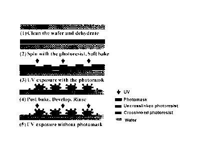
[0015] Figure 1
shows a schematic of a photolithography process for the
fabrication of micro-/nano-scale hierarchical structures on regular surfaces;
zo [0016] Figure
2 shows a schematic of a photolithography process for the
fabrication of micro-/nano-scale hierarchical structures on surfaces, which
strongly
absorb UV;
[0017] Figure 3
shows a schematic of HMDS treatment of substrates for
improved adhesion of photoresist to substrates;
[0018] Figure 4 shows a schematic of vaporized fluorosilane deposition;
[0019] Figure 5
shows SEM images of the development of the KMPR
photoresist structure as a function of developing time;
[0020] Figure 6a
shows nanoparticles with a photoresist (SU-8) developing
time of 90 sec (scale bars in the figures stand for 1 pm);
[0021] Figure 6b
shows nanoparticles with a photoresist (SU-8) developing
time of 60 sec (scale bars in the figures stand for 1 pm);
[0022] Figure 6c
shows nanoparticles with a photoresist (SU-8) developing
time of 30 sec (scale bars in the figures stand for 1 pm);
4
CA 02877244 2014-12-18
WO 2013/188958 PCT/CA2013/000583
[0023]
Figures 7a-b show SEM images of the modified surface of an Si wafer;
[0024]
Figures 7c-d show SEM images of the modified surface of a black filled
Butyl rubber;
[0025]
Figures 7e-f show SEM images of the modified surface of a white filled
Butyl rubber;
[0026]
Figure 8 shows the contact angles vs. area fractions of pillars with
nanoparticles and "bare" pillars; and,
[0027]
Figure 9 shows a schematic of a photolithography process for the
fabrication of micro-/nano-scale hierarchical structures on metallic surfaces.
Detailed Description
[0028]
Measuring the contact angle 0 (CA) is one way to characterize wetting
of surfaces. The CA is affected both by the chemical nature of the surface and
by its
roughness. Affinity of a flat surface towards a certain liquid is defined in
terms of the
"flat" (or intrinsic, or Young's) contact angle,
cos(Ofõõ ) = - (1)
YLA
where y is the surface energy (or surface tension), subscript S stands for
solid, L for
liquid and A for air. The solid-liquid surface energy can be estimated via the
other
two as follows:
YJ 15A YL4-2,irs4r (2)
[0029] The
surface is called (hydro-, oleo-, etc.) -phobic ift9 > 90 , and -philic
otherwise. For water (surface energy yba= 73 mJ m-2) the best non-wetting
situation
on a flat surface is achieved if it is terminated with -CF3 groups, which
brings its
surface energy down to SA"' 6 mJ m-2. The value of intrinsic (Young's) contact
angle
for water on such a surface is O -120 [which is close to the estimation via
the
Eqs. (1) and (2)]. By contrast, most oils have very low surface energies (e.g.
yLA =
27.6 mJ m-2 for hexadecane, yLA = 23.8 mJ rr1-2 for decane). Consequently,
even on
the chemically least energetic -CF3 terminated surface, the intrinsic
(Young's)
contact angle for a typical oil such as hexadecane is 0 - 78 . In other words,
flat
surfaces are intrinsically oleophilic, according to Young's contact angle, no
matter
5
CA 02877244 2014-12-18
WO 2013/188958 PCT/CA2013/000583
what the chemical nature is of the flat surface. This circumstance has
profound
consequences on the design of super-oleophobic surfaces.
[0030] The
term "superhydrophobic" as used herein comprises surfaces
having a contact angle for water of greater than 1500
.
[0031] The term "superoleophobic" as used herein comprises surfaces having
a contact angle for an organic liquid of greater than 150 . Such organic
liquids may
comprise hydrocarbon liquids having a surface energy yLA < 30 mJ nn-2. Such
liquid
hydrocarbons may be characterized as hydrophobic and may be liquid at ambient
temperature and pressure. Such liquids may comprise aliphatic hydrocarbons
having from 6 to 14 carbon atoms, for example octane, decane or hexadecane. A
preferred organic liquid for the purposes of defining superoleophobicity
herein is
hexadecane.
[0032] The
term "substrate" as used herein comprises a material having a
surface amenable to modification in order to impart desired superoleophobic
properties. Preferred substrates are those having surfaces amenable to
modification
using the photolithographic processes described herein. Suitable substrates
may be
organic or inorganic. Examples of suitable substrates may include silicon,
glass,
metal or polymer materials. The metal materials may comprise tri-valent or
penta-
valent metals, such as aluminum or gold. The polymer materials may comprise an
elastomer or a rubber. The rubber may comprise styrene-butadiene,
polybutadiene,
ethylene-propylene diene monomer (EPDM), nitrile or butyl rubber.
[0033] The
term "butyl rubber" as used herein comprises a copolymer of an
isoolefin monomer and a multiolefin monomer, optionally in the presence of
further
copolymerizable monomers. The copolymer may be substituted with one or more
functional groups and may be halogenated. Examples of suitable isoolefin
monomers include isoolefins within the range of from 4 to 16 carbon atoms,
preferably 4-7 carbon atoms, such as isobutene, 2-methyl-1-butene, 3-methy1-1-
butene, 2-methyl-2-butene, 4-methyll-pentene and mixtures thereof. Isobutene
is
one example of a preferred isoolefin. Suitable multiolefin monomers may
comprise
conjugated diene monomers having in the range of from 4-14 carbon atoms, for
example isoprene, butadiene, 2-methylbutadiene, 2,4-dimethylbutadiene,
piperyline,
3-methyl-1,3-pentadiene, 2,4-hexadiene, 2-neopentylbutadiene, 2-methly-1,5-
hexadiene, 2,5-dimethly-2,4-hexadiene, 2-methyl-1,4-pentadiene, 2-methy1-1,6-
heptadiene, cyclopenta-diene, methylcyclopentadiene, cyclohexadiene, 1-vinyl-
cyclohexadiene and mixtures thereof. Isoprene is one example of a preferred
conjugated diene.
Suitable multiolefin monomers may also comprise
cyclopentadiene, nnethylcyclopentadiene and/or styrenic monomers, for example
6
CA 02877244 2014-12-18
WO 2013/188958 PCT/CA2013/000583
styrene, chloro-styrene, alpha-methyl styrene or para-methyl styrene. The term
"butyl rubber" may also include, for example, random copolymers of
isobutylene,
isoprene and para-methylstryene.
Commercially available butyl rubbers are
provided by LANXESS Inc. under the tradenames RB-301 TM, RB-401 TM, BB-2030TM,
etc.
[0034] The
term "microscale" as used herein comprises a surface having a
measurable feature in the range of from 1 to 999 pm.
[0035] The
term "nanoscale" as used herein comprises a surface having a
measurable feature in the range of from 1 to 999 nm.
[0036] The term "multiscale" as used herein comprises a surface having two
or more measurable features, at least one of which is microscale and at least
one of
which is nanoscale.
[0037] The
term "pillar" as used herein comprises a measurable surface
feature having an aspect ratio of height to narrowest width (or diameter) of
greater
than 1, greater than 1.5, greater than 2, greater than 3, greater than 4,
greater than
5, greater than 10, greater than 15, greater than 20 or in the range of from 1
to 20,
1.5 to 18 or 2 to 15. Pillars may be square, rectangular or cylindrical in
cross-
sectional shape and may have a uniform cross-sectional shape along at least a
portion of their height.
[0038] The term "re-entrant" as used herein comprises a surface feature
that
has a first portion with a first width and a second portion with a second
width, the
first width greater than the second width. One example of a re-entrant surface
feature is provided by a plurality of nanoparticles aggregated atop a
micropillar such
that a composite top is formed having a diameter larger than that of the
pillar. Re-
entrant features preferably have a convex upper surface. Re-entrant surface
features may resemble "mushroom caps", "bean sprouts", "hoodoos", or a variety
of
other similar commonly known shapes when seen in side view.
[0039] The
term "nanoparticle" as used herein comprises a nanoscale deposit
of a heterogeneous material. Nanoparticles may be regular or irregular in
shape and
may be formed from a plurality of co-deposited particles that form a composite
nanoscale particle. Nanoparticles may be generally spherical in shape or have
a
composite shape formed from a plurality of co-deposited generally spherical
particles. Suitable materials for formation of a nanoparticle may comprise
negative
photoresists that are initially uncrosslinked.
7
[0040] The term
"fluorinated hydrocarbon" as used herein comprises a
fluorine substituted hydrocarbon that may be aliphatic, aromatic or polymeric
in
nature and may additionally be substituted with other organic moieties.
Examples of
a fluorine substituent are ¨CF2H,-C6F5, ¨CF2 and ¨CF3. Suitable fluorinated
hydrocarbons may be those that are amenable to vapour deposition. An example
of
a suitable fluorinated hydrocarbon is a silane substituted fluorinated
polymer, or
fluorosilane, such as 1H,1H,2H,2H-perfluoroctyl-trichlorosilane, 1H,1H,2H,2H-
perfluorodecyltrimethoxysilane, and 1H, 1H,2H ,2H-
perfluorodecyltrichlorosilane.
[0041] The term
"photolithography" as used herein comprises optical
lithography techniques that use light to selectively remove material from or
add
material to a substrate. Photolithographic processes may comprise the
application
of a photoresist to the substrate. The photoresist may be a chemical that is
sensitive
to light of a particular wavelength being applied to the substrate. The
photoresist
may be a positive photoresist that reacts with the light and becomes soluble
in the
developer or a negative photoresist that reacts with the light to become
crosslinked
and insoluble in the developer. Negative photoresists suitable for use herein
are
those that polymerize upon exposure to ultraviolet light, for example epoxy
based
photoresists comprising an epoxy resin, an organic solvent, and a cationic
photoinitiator, such as KMPR or SU-8, as described in US Patent 4,882,245.
Persons of skill in the art are familiar with other
epoxy based photoresists that function in a similar manner. A pattern may be
created on the substrate by using a photomask to selectively block light from
interacting with the photoresist in desired locations. In this
manner, a desired
pattern of polymerized material may be built on the surface of the substrate.
A
developer may be used to remove or wash away uncrosslinked or unpolymerized
negative photoresist. The washing with developer may be conducted for a pre-
determined time period selected in order to leave residual uncrosslinked or
unpolymerized photoresist on the substrate. For example, the time period may
be
from 45 to 75 seconds for a specific thickness of photoresist layer and
particular
washing conditions. The time period may be abbreviated as compared with
conventional photolithographic processes, which normally seek to remove all
uncrosslinked photoresist.
Photolithograhic processes may comprise multiple
iterations in order to increase the size of the desired surface features.
Further
information on photolithographic techniques suitable for use with the present
invention may be found in Marc J. Madou, Fundamentals of Microfabrication: The
Science of Miniaturization, Second Edition, New York: CRC Press, 2002.
8
CA 2877244 2019-09-12
CA 02877244 2014-12-18
WO 2013/188958 PCT/CA2013/000583
[0042]
After developing, the process may further comprise washing the
residual photoresist developer in an alcohol, for example a short chain
alcohol or
iso-alcohol, such as isopropanol. The washing step may serve to nucleate the
uncrosslinked photoresist atop the micropillars. This step may optionally be
followed
by a further aqueous wash step to remove residual alcohol, for example with DI
water. The sample may be exposed again to ultraviolet light without using the
photomask, thereby crosslinking the residual photoresist nucleated atop the
micropillars into nanoparticles that are optionally crosslinked also to the
micropillars.
[0043] The
term "vapour deposition" as used herein comprises physical or
to chemical vapour deposition. A preferred form of vapour deposition is
molecular
vapour deposition. Vapour deposition processes may employ a volatile solvent
that
acts as a carrier for the material to be deposited. The solvent may be removed
by
elevated temperature and/or reduced pressure. The elevated temperature may be
greater than 50 C, greater than 60 C, or greater than 80 C. The elevated
temperature may be in the range of from 50 to 120 C, 55 to 100 C, 60 to 90
C or
65 to 85 C. Suitable materials for vapour deposition are those that do not
decompose under process temperature and those that adhere in some fashion to
the substrate. The material may adhere to the substrate or other materials
adhered
to the substrate by physical adsorption. The material may be a fluorinated
molecule
such as a fluorinated hydrocarbon that may physically adhere to or chemically
react
with the nanoparticles and/or micropillars.
[0044] The
area fraction, f, of the surface may be important for providing
desirable superoleophobic properties. It may be desirable to provide the
substrate
with an area fraction in the range of from 0.01 to 0.20, or from 0.01 to 0.15,
or from
0.01 to 0.10, or from 0.05 to 0.10, or from 0.02 to 0.09, or from 0.03 to
0.08, or from
0.04 to 0.07, or from 0.05 to 0.06.
[0045]
When rubber is used as a substrate, a larger dose of ultraviolet
radiation may be required to initiate the crosslinking reaction than would be
required
for silicon substrates under otherwise identical conditions. In order to
attenuate the
ultraviolet light applied to the substrate surface, it may be desirable to
apply a thin
layer of negative photoresist prior to the photolithography process and
exposing
substantially the entire surface to a lower dosage of ultraviolet light.
This
polymerizes a layer of photoresist on the substrate in order to improve
adhesion of
subsequently formed features and also to protect the substrate from the higher
doses of ultraviolet light required in subsequent stages of the process.
[0046] In
order to further increase adhesion of the photoresist to the
substrate, particularly when polymeric or rubber substrates are used, it may
be
9
desirable to pretreat the substrate with a hexamethyldisilazane (HMDS) prior
to
application of the photoresist.
[0047] In order to create superoleophobic surfaces at commercial
scale, a
variety of techniques can be used. One such technique employs large-area roll-
to-
roll and roll-to-plane nanolithography technology that is based on near-field
optical
lithography using cylindrically shaped rolling masks. Such techniques are
described
in, for example Ahn, S.H. and L.J. Guo, Large-Area Roll-to-Roll and Roll-to-
Plate
Nanoimprint Lithography: A Step toward High-Throughput Application of
Continuous
Nanoimprinting. ACS nano, 2009. 3(8): p. 2304-2310..
[0048] Substrates comprising the superoleophobic surface morphology
may
be formed into useful articles or applied to previously shaped articles in the
form of a
coating, overnnold or the like. This imparts useful barrier properties to the
article,
such as resistance to penetration or attack by organic liquids, such as
hydrocarbons,
or the like. Other applications include fat and oil resistant coatings for
articles in the
medical device or pharmaceutical industry. Numerous other applications may be
conceived by those skilled in the art.
Examples
Materials and Methods
[0049] Negative photoresist SU-8 (epoxy resin, cyclopentanone as organic
solvent, triarylsulfonium salt as a cationic photoinitiator), negative
photoresist KMPR
(modified epoxy resin, cyclopentanone, triarylsulfonium, propylene carbonate)
and
SU-8 developer (1-Methoxy-2-propyl acetate) were purchased from MicroChem
Corporation, Newton, MA, USA. 1H,1H,2H,2H-perfluoroctyl-trichlorosilane (97%)
zs was a product from Sigma-Aldrich. Piranha solution was made using H202
(30%)
and H2504 (conc) solution in 3:7 vol/vol ratio. All of the chemicals were used
as
received. Patterns on photomasks were designed using the 1-Edit software and
then
printed on chromium glasses with a high-resolution image-setting system
(Nanofab,
Alberta University). A spin coater (Solitec 5110 Spinner) and a mask aligner
(Karl
Suss MA6) were available in the Western Nanofabrication Lab at the University
of
Western Ontario. All processing solutions were prepared with the de-ionized
(DI)
water from a Milli-Q system (Millipore, Bedford, MA) filtered through 0.2 pm
filters
(Millipore).
CA 2877244 2019-09-12
CA 02877244 2014-12-18
WO 2013/188958 PCT/CA2013/000583
Fabrication of micro-/nano-scale hierarchical structures
[0050] Referring to Figures 1, 2 and 9, the fabrication of a surface
with
multiscale structures was performed as follows. The substrates were first
carefully
cleaned in the piranha solution (80 C) for 20 minutes, and dried at 100 C for
5
minutes on a hotplate. The negative photoresist (SU-8 3010) was poured onto
the
substrates and spread using a spin coater at 500 rpm for 5 seconds followed by
1000 rpm for 30 seconds. Soft baking at 95 C on hotplate was carried out for
10
minutes to remove the excess solvent from the SU-8 layer. Then the SU-8 layer
was
cross-linked via ultraviolet (UV) light exposure through a photomask using a
mask
aligner (sensor wavelength = 365 nm, UV intensity 6 mW/cm2). See Table 1 for
UV
exposure times. Polymerization of SU-8 was conducted in the post-exposure bake
at
65 C for 1 minute and 95 C for 3 minutes. The samples were developed in SU-8
developer to dissolve uncross-linked resist, for a period shorter than the
time
normally required to fully remove or wash away all of the uncrosslinked
photoresist.
This resulted in residual uncross-linked photoresist creating the hierarchical
structure. Regarding the experimental parameters above, the shortened
development time was 45 seconds. Then, the samples were immersed in
isopropanol, in which a visible film was formed on the SU-8 structure. The
residual
isopropanol was washed away using de-ionized water. Finally, the sample was
exposed without the photomask under a regular UV lamp for 30 seconds. An
alternative would be to use sunlight, which also contains UV light. The
fabrication
steps with KMPR as the negative photoresist were the same, except that the
spinning speed, exposure dose and baking time needed to be adjusted. Figure 1
shows a schematic of the photolithography process for the fabrication of a
superoleophobic surface.
[0051] The multiscale structures can be fabricated on a wide variety
of
different substrate materials using similar fabrication steps to those
described above.
Schematics of the process used with a variety of different substrates are
shown in
Figures 1, 2 and 9. The major process difference between different substrate
materials is the UV exposure required, due to their diverse UV reflectivity
and
absorbance. For example, the rubber substrates require a higher UV dose as
compared with the silicon (Si) wafers (see Table 1 for representative doses).
The UV
beams propagate through the photoresist layer to the substrate. Most of the
beams
are reflected by the Si substrate and pass through the photoresist again. In
contrast,
a large amount of UV energy is absorbed and fewer beams bounce back through
the
photoresist if the substrate is rubber. If the UV dose is too great, a size
mismatch
occurs between the pillar structure and its photomask pattern. Referring to
Figure 2,
for polymer surfaces an ultrathin layer of flat photoresist is applied before
building
11
CA 02877244 2014-12-18
WO 2013/188958 PCT/CA2013/000583
the actual structures to attenuate the UV absorption by the substrate. Due to
the
difference between surface adhesion and thermal conductivity, the spinning
speed,
baking time and developing time need to be adjusted according to the specific
substrate. In addition, many materials easily oxidize, so long range hydrogen
bonds
form on the surface oxide with water adsorbed from the air. Once the resist is
spun
onto such a surface, it adheres to the water vapor rather than to the surface,
resulting in poor adhesion. The substrates can be treated with HMDS
(Hexamethyldisilazane) vapor (YES-3TA HMDS Oven) for increased adhesion of the
photoresist (Figure 3).
Chemical modification of surfaces
[0052]
Once the multiscale structure was built up on the substrate, the sample
was fluorinated via vaporized 1H,1H,2H,2H-perfluoroctyl-trichlorosilane.
Droplets of
silane were applied around the sample in a covered Petri dish. Care was taken
to
avoid any direct contact of droplets with the samples. The Petri dish was
baked at
80 C on a hotplate to vaporize fluorosilane for 20 minutes. After that, the
cover of
the Petri dish was removed, leaving the samples to completely dry out at the
room
temperature (Figure 4).
Results and Discussion
Surface topography and chemical modification
[0053] Photolithography using a negative photoresist is a robust method to
fabricate micro-structures, which possesses stable chemical resistance, good
thermal endurance for up to 200 C, and mechanical performance with Young's
modulus 4-5 GPa (for SU-8). With the experimental parameters presented above,
uniform photoresist micro-pillar arrays were fabricated on a Si wafer with a
height of
20 pm (related to the resist coating speed and surface adhesion of
substrates). The
area fraction (f) of this superoleophobic surface was changed by varying the
diameter of pillars from 7 pm to 15 pm, but keeping the center to center
distance 25
pm. The nanoparticles were formed from un-crosslinked photoresist, SU-8
developer
and isopropanol. Based on the liquid-liquid nucleation process, or so called
Ouzo
effect, a milky oil-in-water microennulsion forms when water is added to Ouzo
(ethanol). In the present configuration, the negative photoresist, developer
and
isopropanol perform a similar function as the oil, ethanol and water in Ouzo,
respectively. When mixing with isoproponal, the negative photoresist becomes
greatly supersaturated, leading to the nucleation of photoresist droplets.
Meanwhile,
the photoresist immediately begins migrating to the adjacent droplet, so that
the
supersaturation decreases and no further nucleation occurs. In the
conventional
12
CA 02877244 2014-12-18
WO 2013/188958 PCT/CA2013/000583
photolithography process, the uncrosslinked photoresist is dissolved in SU-8
developer, leaving the crosslinked structure, which is the pillar array in our
design.
However, the present process employs a shorter pre-determined developing time
(under-developed), so that a small amount of un-crosslinked photoresist
remains on
the surface of the pillar array. Once this sample is dipped in isopropanol,
the un-
crosslinked photoresist is shaped into spherical nanoparticles. Since the
micropillars
are hydrophobic, these nanoparticles mostly congregate around the top of
pillars
instead of filling the gap between pillars, so that a re-entrant structure is
formed by
these clustered convex nanoparticles. The development of the photoresist (SU-8
or
io KMPR) nanoparticle structure as a function of developing time is
demonstrated in
Figure 5. The size of the nanoparticles is adjustable by changing the
developing
time. The shorter the developing time, the larger the particle size produced
(Figure
6a-6c). The control of the nanoparticles size may help to further improve the
superoleophobicity. Therefore, the re-entrant structure over pillars can be
easily
manipulated for maximum superoleophobic performance.
[0054] In addition, the negative photoresist intrinsically possesses
high
surface adhesion to various substrates, thus the micropillars are very stable
and well
attached to the base. The bonding between micropillars and nanoparticles is
also
very strong, as the nanoparticles are also made of negative photoresist and
are
crosslinked to the pillars. The textured surfaces made on Si wafer, white
filled and
black filled butyl rubbers are shown in Figure 7a-7f.
[0055] Fluorination of the artificial structure was carried out under
regular
laboratory conditions without the elimination of oxygen and moisture in order
to
simplify the fabrication process. Fluorination lowers the surface energy by
increasing
the concentration of ¨CF3 chemical groups at the surface. Even though for all
oils on
all flat surfaces, Ol <9O, one generally wants to increase the intrinsic
contact angle
(CA) as much as possible. A smaller degree of reentrancy is needed the closer
the
CA is to 90 degrees. Thus, the energetic difference between metastable
(superoleophobic) and stable (complete wetting) states should be smaller. It
is also
expected that lower surface energies will provide higher barriers for
transition from
Cassie-Baxter to Wentzel states, leading to increased robustness. Since the
fluorocarbon groups (especially -CF3) are known to possess low surface
energies,
rough surfaces should benefit from being fluorinated.
Super - hydro/oleo - phobicity
[0056] The contact angle for these surfaces with water is always nearly 180
,
while the results for hexadecane changed with f of pillar tops (relatively to
the total
13
CA 02877244 2014-12-18
WO 2013/188958 PCT/CA2013/000583
surface area). As shown in Figure 8 (red line and circular knob), the contact
angle
for hexadecane was only 135 when f was 0.25. The surface exhibits higher oil
repellency at lower values of f(160 for f around 0.05). This tendency
corresponds to
the Cassie - Baxter equation for heterogeneous wetting:
co s emugh = f cos 0/10, - (1-
(3)
[0057] where f is the area fraction of solid surface which is in
contact with the
liquid,
rough and Gib, are the contact angles for the rough surface and flat surface,
respectively. Therefore, the contact angle with hexadecane reached 160 (and
with
methanol was 120 ) by minimizing the area fraction. The droplets easily rolled
off the
surface, indicating a small contact hysteresis. Although SU-8 itself is
hydrophobic,
hexadecane easily wetted the flat SU-8 surface. Surfaces only patterned with
micro-
scale pillars had a lower repellency to oil than surfaces comprising both
micropillars
and nanoparticles (Figure 8, black line and squares). These controlled
experiments
illustrate the importance of area fraction to the superoleophobicity of the
surface.
The properties of different substrates are shown in Table 1.
[0058]
Table 1. Properties of different substrates.
Substrate Photoresist UV Static contact Static contact
Tape test
exposure angle angle (Methanol) (until
hexadecane
(Seconds) (Hexadecane)
droplet cannot roll
off)
Silicon SU-8 33 160=0.6 120-10.8 Average 7 times
(Scotch tape)
Black-filled SU-8 60 158 0.8 N/A Average 5 times
IIR (Nichiban tape)
White-filled SU-8 60 157 0.6 N/A Average 5 times
IIR (Nichiban tape)
Gold SU-8 30 156-10.6 N/A N/A
Aluminum SU-8 30 157 0.8 N/A N/A
Silicon KMPR 50 163-10.6 N/A N/A
substrate
14
CA 02877244 2014-12-18
WO 2013/188958 PCT/CA2013/000583
Discussion
[0059] It
has been shown in the above examples that multiscale roughness
features ranging from hundreds of microns for pillars in combination with
those in the
range of tens of nanometers for particles are important to produce
superoleophobic
coatings. The reason for this is two-fold. Firstly, such multiscale roughness
can
make the surface very "airy", and thus decrease the effective liquid-solid
contact
area fraction f in Eq. (3). Secondly, it is important to produce a re-entrant
and convex
morphology.
[0060] Prior art microscale surfaces share one significant drawback - they
only have one re-entrant feature per valley. This means that if the surface
has a
defect or local disturbance on one of the re-entrant features, a liquid drop
will most-
likely wet the local valley. By contrast, the present surfaces are more robust
because
there are many re-entrant features associated with each valley. This greatly
improves the probability that a liquid drop will not wet the present surfaces.
[0061] In
summary, a re-entrant surface curvature (nanoparticles), in
conjunction with roughened texture (micropillars) can be used to design
surfaces
that display extreme resistance to wetting from a number of liquids with low
surface
tension, including hexadecane and methanol. SU-8 and KMPR are simply examples
of negative photoresists; it is probable that other types of negative
photoresist can
also be used in the fabrication of these superoleophobic surfaces.
[0062]
Disclosed herein is a simple and fast fabrication method to produce
superoleophobic surfaces using only photolithography and a simple fluorosilane
vapor deposition technique. The multiscale morphology of such superoleophobic
surfaces combines both micro-scale regular pattern (pillars) as well as nano-
scale
roughness (via assemblies of nanoparticles). This method can be applied to
various
kinds of substrates materials including silicon wafers, glass wafers, metal
sheets and
thin rubber films. The resulting superoleophobic surfaces are robust and
stable.
Furthermore, the fabrication technique disclosed herein is simple and low-cost
as
compared with many other methods, and thus suitable for practical
applications.