Note: Descriptions are shown in the official language in which they were submitted.
CA 02877440 2014-12-19
WO 2014/006200 PCT/EP2013/064297
DESCRIPTION
Controlling a modular converter
FIELD OF THE INVENTION
The invention relates to a method for controlling a modular converter, a
controller for
controlling a modular converter and a modular converter.
BACKGROUND OF THE INVENTION
Electrical converters, in particular in the medium and high voltage area, are
used for
converting a first current with a first frequency and a first voltage into a
second current
with a second frequency and a second voltage. Many types of converters are
known such
as for converting AC to AC, AC to DC, DC to AC and DC to DC.
Usually, converters comprise high power semiconductors for switching
internally
currents to produce the desired output current. In modular converters, these
power
semiconductors are distributed among converter modules, which also may
comprise further
components like a controller for the semiconductors or a capacitor for storing
energy in the
converter module.
For example, the M2LC topology has become popular in both medium and high
voltage
applications. An M2LC converter or modular multi-level converter comprises
converter
arms with converter modules connected in series for generating a multi-level
output
voltage. In an M2LC converter the converter modules each comprise a capacitor
themselves.
The standard approach to achieve closed-loop control for an M2LC converter is
to
divide the control problem into two hierarchical layers. The upper layer is
based on vector
control with a modulator. The vector control scheme operates in a orthogonal
reference
frame rotating with a certain angular velocity. By manipulating the voltage
reference to the
modulator, closed-loop control of the load currents can be achieved.
Typically, carrier-
based pulse width modulation (PWM) or space vector modulation (SVM) is used as
CH-12063-WO-PCT /05.07.2013 / OF
CA 02877440 2014-12-19
WO 2014/006200 PCT/EP2013/064297
2
modulator. The circulating currents and/or the energy balance within the
converter arms
may be addressed by adding additional control loops.
The lower control layer utilizes the redundancy in the converter states (e.g.
groups of
switching states that produce the same line to line voltage, and/or groups of
switching
states that produce the same arm voltage) in order to balance the capacitor
voltages. The
capacitor voltages are sorted in an ascending/descending order of their
voltage values. For
a charging current the capacitors with the lowest voltages are selected first,
and conversely,
the capacitors with the highest voltages are prioritized for discharging
currents.
DESCRIPTION OF THE INVENTION
It is an objective of the invention to provide an alternative solution for
controlling a
modular converter, to reduce the switching losses of a modular converter, to
balance the
capacitor voltages, and to reduce harmonics in the input and output currents
of a modular
converter.
It is a further objective of the invention to provide a control schema with
good
performance during steady-state as well as during transient operating
conditions.
These objectives are achieved by the subject-matter of the independent claims.
Further
exemplary embodiments are evident from the dependent claims and the following
description.
An aspect of the invention relates to a method for controlling a modular
converter with
a plurality of converter modules. A converter module may comprise a number of
power
semiconductors and optionally a capacitor or more generally an energy storage
and/or an
energy source. For example, the power semiconductors are interconnected in
such a way,
that two power connectors of each of the modules may be short-circuited in a
first
switching state and may be connected to the energy storage and/or the energy
source in a
second switching state.
The method comprises the steps of: selecting possible future switching
sequences,
predicting a future current trajectory for each switching sequence,
determining candidate
sequences from the switching sequences, predicting future module voltages for
each
candidate sequence, evaluating a cost function for each candidate sequence and
selecting
the next converter switching state based on the result of the cost function.
CH-12063-WO-PCT /05.07.2013 / OF
CA 02877440 2014-12-19
WO 2014/006200 PCT/EP2013/064297
3
The possible future switching sequences of the converter are selected based on
an actual
converter switching state, wherein a switching sequence is a series of
converter switching
states with at least one converter switching state and a converter switching
state comprises
switching states of the converter modules.
The future current trajectory for each switching sequence is predicted based
on actual
internal currents of the modular converter and on actual internal voltages of
the modular
converter. The current trajectory may be a trajectory of a load current, an
arm current or a
circulating current. The future current trajectory may be predicted for more
than one time
step in the future. For example, the actual internal currents comprise arm
currents and/or a
DC link current and/or circulating currents, the actual internal voltages may
comprise
phase voltages and/or arm voltages and/or the DC liffl( voltage. For example,
based on an
internal state-space model of the converter, the trajectories of key system
variables, such as
load currents, circulating currents and/or capacitor voltages, are predicted
for all
admissible switching sequences.
The candidate sequences are determined from the switching sequences such that
a
candidate sequence is a switching sequence with a current trajectory that
respects
predefined bounds with respect to a reference current or, when a predefined
bound is
violated, moves the current trajectory closer to the predefined bound. For
example, a load
current may be kept within symmetrical bounds around its sinusoidal
references. The total
harmonic distortion of the current may be adjusted by varying the width of the
predefined
bounds. The relationship between the total harmonic distortion and the bound
width is
usually effectively linear.
Switching sequences that keep the load currents within their bounds or move
them
closer to the bounds (when they are violated) are determined and called
candidates. These
candidate trajectories are extrapolated or extended until a certain criterion
is met such as
the violation of a hysteresis bound. At this point new switching vectors can
be considered
and another extrapolation step can be performed, and so on.
The future module voltages for each candidate sequence are predicted based on
actual
module voltages and the current trajectory of the respective candidate
sequence. For
example, from predicted currents and the switching states the voltage between
the outputs
of a converter module and/or across a capacitor of the converter module may be
calculated.
The cost function is evaluated for each candidate sequence. The cost function
is based
on the converter switching states of the switching sequence, the future module
voltages and
CH-12063-WO-PCT /05.07.2013 / OF
CA 02877440 2014-12-19
WO 2014/006200 PCT/EP2013/064297
4
or future currents. For example, the value of the cost function may be based
on the number
of switchings between switching states and/or the switching losses caused by
the
switchings of a switching sequence. In general, the cost function may include
the predicted
short-term switching frequency (or switching losses), the violation of the
current bounds,
the deviation of the capacitor voltages from their references, the mismatch
between
capacitor voltages within an arm, etc. The future currents may be internal
current
determined for the current trajectories and/or may be future load currents.
The next converter switching state is selected as the first converter
switching state of a
candidate sequence with minimal costs. Minimizing the cost function yields the
optimal
switching vector. At the next sampling instant, new measurements or estimates
may be
obtained and the above described optimization process may be repeated over a
shifted
horizon, according to a so-called receding horizon policy. With the method,
the switching
states are manipulated directly. An intermediate stage, such as a modulator,
is not required.
The method features an online optimization process to determine the future
control
inputs, without using a modulation stage, to directly control the load
currents and offers a
great flexibility to handle various system objectives.
The method may be implemented in a controller with only a single control loop,
while
the considered currents are kept within upper and lower bounds around their
references.
The method has the advantages of direct current control without a modulation
stage, of
a fixed and controlled ripple of the load currents, and of very short response
times during
transients. At steady-state, the desired trade-off may be set by the weights
in the cost
function.
Furthermore, the capacitor voltages may be balanced around their nominal
voltages. In
this case, the energy stored in the converter may be controlled, the converter
modules may
be equally voltage stressed, the arm currents may be optimized, circulating
currents may be
reduced, and conduction losses are lowered.
At steady-state operating conditions and for a given load current distortion,
the lowest
possible switching frequency may be achieved.
According to an embodiment of the invention, each converter module has exactly
two
power connectors which are short-circuited in the first switching state of the
semiconductors and are connected to the energy storage and/or energy source in
the second
switching state of the semiconductors.
CH-12063-WO-PCT /05.07.2013 / OF
CA 02877440 2014-12-19
WO 2014/006200 PCT/EP2013/064297
According to an embodiment of the invention, the cost function is based on a
number of
switching operations between two consecutive converter switching states. In
such a way,
the number of switching operations may be reduced or minimized.
According to an embodiment of the invention, the cost function is based on a
difference
5 between module voltages of converter modules of a converter arm
comprising at least two
converter modules connected in series. In such a way, the differences between
capacitor
voltages may be minimized.
According to an embodiment of the invention, the cost function is based on a
difference
between a module voltage and a supply voltage at an input of the converter. In
such a way,
a reference value for the phase voltage may be set and ripples around the
reference value
may be reduced.
According to an further embodiment of the invention, the cost function is
based on a
difference between a module voltage and a supply voltage of the converter
divided by the
number of modules per arm. In such a way, a reference value for the phase
voltage may be
set and ripples around the reference value may be reduced.
According to an embodiment of the invention, the cost function is based on a
difference
between the sum of module voltages of a first converter arm for a phase and
the sum of
module voltages of a second converter arm for the same phase or a different
phase. In such
a way, the imbalance in capacitor voltages of different converter arms may be
minimized.
According to an embodiment of the invention, the cost function is based on a
difference
between the sum of module voltages of a first phase and the sum of module
voltages of a
second phase. In such a way, the imbalance in capacitor voltages of different
converter
phases may be minimized.
According to an embodiment of the invention, the method further comprises the
step of:
deselecting candidate sequences for which future module voltages do not stay
within
predefined bounds. Also the module voltages may be constrained to predefined
bounds.
Furthermore, the number of admissible candidate sequences may be reduced on
which the
cost function has to be evaluated.
According to an embodiment of the invention, each converter module comprises a
module capacitor. In particular, a modular multi-level converter may comprise
converter
modules with a capacitor that is adapted for storing energy in the converter
module. The
module voltages that are predicted and optimized with the method may be
capacitor
voltages over module capacitors.
CH-12063-WO-PCT /05.07.2013 / OF
CA 02877440 2014-12-19
WO 2014/006200 PCT/EP2013/064297
6
According to an embodiment of the invention, a switching sequence comprises a
switching step associated with a converter switching state, in which switching
step the
future current of the converter is predicted when switching the converter into
the
associated converter switching state; and /or a switching sequence comprises
an
extrapolation step, in which the load current is extrapolated over at least
one time step until
it violates the bounds for the load current. In general, a switching sequence
may comprise a
plurality of steps which either are switching steps or extrapolation steps.
The set of switching sequences determined by the method may be established by
using
the notion of S ("switch") and E ("extend", "extrapolate"), forming the
switching horizon.
The switching horizon may comprise any combination of S and E steps. The
extrapolation
step may be approximated, for example using linear or quadratic extrapolation,
or
prediction with quadratic interpolation. Higher order approximations are
possible, too. The
notion of switch and extend achieves long prediction horizons, and therefore
better steady-
state performance, while using a short switching horizon, ensuring that the
computational
burden is kept at bay. The switching horizon may be composed of an arbitrary
sequence of
elements S and E.
According to an embodiment of the invention, the future current trajectory is
predicted
based on a first internal model of the converter. The future module voltages
may be
predicted based on a second internal model of the converter, which is
dependent on the
first internal model. The two internal models may be state space models of the
converter.
The first model may capture the evolution of the currents, including the load
and the
circulating currents, while the second model may capture the evolution of the
capacitor
voltages. The second model may be dependent on the first model in such a way,
that it is
based on values predicted by the first model. For example, the two models may
be
expressed as matrix equations and/or may be linear models.
The first model may be based on linear equations between future currents,
actual
currents, actual internal voltages and switching states.
The second model may be based on linear equations between future internal
voltages,
actual internal voltages, actual currents and switching states
According to an embodiment of the invention, the method further comprises the
steps
of: changing the converter topology by bypassing a converter module; and
adapting the
first and/or the second model to the changed converter topology. The converter
modules of
the converter may be monitored in real-time. If a module fails and its
terminals have to be
CH-12063-WO-PCT /05.07.2013 / OF
CA 02877440 2014-12-19
WO 2014/006200 PCT/EP2013/064297
7
shortened to bypass it, the number of converter modules available is
automatically updated
and the internal prediction models of the controller is adjusted accordingly.
The method
may take into account that one or some converter modules are shortened and
uses only
switching states/sequences that, within the physical limitations of the
converter,
compensate for these shortened converter modules.
A further aspect of the invention relates to a computer program, which, when
being
executed on a processor, is adapted for executing the steps of the method as
described in
the above and in the following. For example, the computer program may be
executed in a
processor of a controller of the modular converter.
A further aspect of the invention relates to a computer-readable medium in
which such a
computer program is stored. A computer-readable medium may be a floppy disk, a
hard
disk, an USB (Universal Serial Bus) storage device, a RAM (Random Access
Memory), a
ROM (Read Only Memory) and an EPROM (Erasable Programmable Read Only
Memory). A computer-readable medium may also be a data communication network,
e.g.
the Internet, which allows downloading a program code.
A further aspect of the invention relates to a controller for controlling a
modular
converter, wherein the controller is adapted for executing the steps of the
method as
described in the above and in the following. The proposed controller may
achieve very fast
current responses during transients, such as power up or down, or faults. This
is in contrast
to methods, which focus on the steady-state operation and are, as a result,
very slow during
transients. The capacitor voltages may be kept more closely to their
references i.e. may be
better balanced. The switching frequency can be reduced, compared to methods
using
PWM or SVM.
For example, the controller comprises a DSP and/or FPGA, in which the method
is
implemented.
A further aspect of the invention relates to a modular converter with a
plurality of
converter modules each having a capacitor; and a controller that is adapted
for executing
the steps of the method as described in the above and in the following.
For example, the modular converter is a modular multi-level (M2LC) converter,
which
may have at least one converter arm with at least two converter modules
connected in
series. In general, the method may be used for any M2LC control problem. It
may be used
in M2LC converters with a few modules per arm. It is applicable to all M2LC
applications,
including variable speed drives, high-voltage direct current transmission,
flexible AC
CH-12063-WO-PCT /05.07.2013 / OF
CA 02877440 2014-12-19
WO 2014/006200 PCT/EP2013/064297
8
transmission systems, static synchronous compensators, grid-interfaces for
battery energy
storage systems or PV modules, traction applications, etc. The control scheme
is highly
flexible allowing one to incorporate and address different control objectives
and operation
requirements.
These and other aspects of the invention will be apparent from and elucidated
with
reference to the embodiments described hereinafter.
BRIEF DESCRIPTION OF THE DRAWINGS
The subject matter of the invention will be explained in more detail in the
following text
with reference to exemplary embodiments which are illustrated in the attached
drawings.
Fig. 1 schematically shows a modular converter according to an embodiment of
the
invention.
Fig. 2 schematically shows a converter module of the converter of Fig .1.
Fig. 3 shows a flow diagram for a method for controlling a modular converter
according
to an embodiment of the invention.
Fig. 4 shows current trajectories according to an embodiment of the invention.
Fig. 5 schematically shows a controller according to an embodiment of the
invention.
Fig. 6 schematically shows a modular converter according to a further
embodiment of
the invention.
Fig. 7 schematically shows a converter module for the converter of Fig. 6.
Fig. 8 schematically shows a modular converter according to a further
embodiment of
the invention.
Fig. 9 schematically shows a modular converter according to a further
embodiment of
the invention.
Fig. 10 schematically shows a modular converter according to a further
embodiment of
the invention.
Fig. 11 schematically shows a modular converter according to a further
embodiment of
the invention.
CH-12063-WO-PCT /05.07.2013 / OF
CA 02877440 2014-12-19
WO 2014/006200 PCT/EP2013/064297
9
Fig. 12 schematically shows a modular converter according to a further
embodiment of
the invention.
Fig. 13 schematically shows a modular converter according to a further
embodiment of
the invention.
In principle, identical parts are provided with the same reference symbols in
the figures.
DETAILED DESCRIPTION OF EXEMPLARY EMBODIMENTS
Topology and internal models for a modular converter
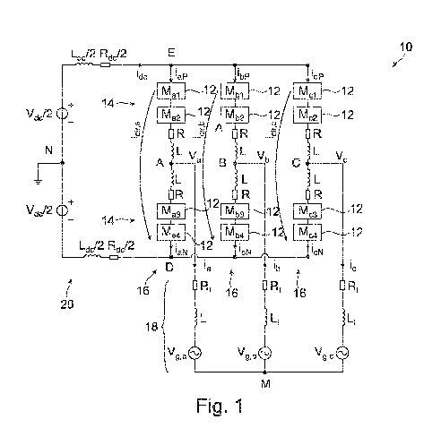
Fig.1 shows the topology of a DC-AC modular multi-level converter 10 with two
converter modules 12 per converter arm 14. The embodiment of Fig. 1 show M=3
converter phases 16 each comprising an upper and a lower converter arm 14.
However, it
has to be understood that embodiments of method described in the above and in
the
following may be applied to converters with an arbitrary number of converter
modules 12
per converter arm 14 and with an arbitrary number of converter phases 16.
In case the converter 10 has N=2 converter modules 12 per converter arm 14 and
three
converter phases 16, the converter has a total of 6N=12 converter modules. The
modules
are referred to by Mpq , p E fa, b, c), q E [1, 2, 3, 4}.
Besides the two converter modules 12, each arm 14 comprises a resistor R that
models
conduction losses and an arm inductor L connected in series with the converter
modules
12.
The two converter arms 14 of a converter phase 16 are connected in series with
a
connection point A, B, C for a load 18, which may be a three phase load. Each
of the
converter phases 16 is connected in parallel to a DC voltage supply 20 via the
connection
points E and D. The DC voltage supply 20 comprises a DC supply inductor Ldc
and a
resistor Rdc that model the parasitic inductance and resistance, respectively.
The current
driven by the DC link voltage of the DC voltage supply 20 is referred to as
the DC link
current idc .
The converter 10 shown in Fig. 1 provides three voltages levels, ¨
v2c/c5 05 _ v2dc, at its
output terminals Va, Vb, Vc, with respect to the supply ground (node N). The
output
terminals Va, Vb, Vc are connected to the load 18. The load 18 shown in Fig. 1
is modeled
by load inductor L1 in series with a load resistor R1 and the grid voltage
Vg,p .
CH-12063-WO-PCT /05.07.2013 / OF
CA 02877440 2014-12-19
WO 2014/006200 PCT/EP2013/064297
Fig. 2 shows a converter module 12 for the converter of Fig. 1. The converter
module
12 comprises two power semiconductor switches Spq,T and Spq,B which are
connected in
series and in parallel to a capacitor Cpq. The converter module 12 acts like a
chopper cell
with the capacitor Cpq. The converter module 12 has two switching states, upq
E [0,11,
5 where 1 means that the capacitor Cpq is connected in the circuit, i.e.
switch Spq,T is on, and
0 means that the capacitor is disconnected from the circuit, i.e. switch Spq,T
is off The
operation of the switches Spq,T, Spq,B is complementary to one another. The
resistor kap is
connected in parallel to the capacitor Cpq to model the leakage current of the
capacitor Cpq
The converter module 12 has two power connectors 21, 22, which are acting as
the
10 input as well as the output of the converter module. Beside the power
connectors 21, 22 the
converter module might have further connections for controlling the converter
module, for
diagnose purposes and other control objectives. The power connectors 21, 22
can either
short circuited or connected to the capacitor by the power semiconductors
switches.
The two power connectors 21, 22 of each converter module are also referred to
as the
inputs. Further, the voltage 17c,pq of the capacitor Cpq is referred to as the
module voltage as
well as capacitor voltage Vc,pq
An embodiment of the method is described hereafter for the specific case of a
three-
level M2LC converter 10 with N=2 modules per arm and M=3 phases. In a
subsequent
section, the approach is generalized.
The output equations for the load current in phases a, b and c are as follows:
ja(t) = jap(t) ¨ jaN(t)
ib(t) = ibp(t) ¨ ibN(t)
ic(t) = ¨ jap(t) + jaN(t) ¨ ibp(t) + ibN(t)
The equation which defines the circulating currents in phases a, b and c is as
follows:
ipp (t) ipN i
-dc
icir,p(t) = ___________________ 2 + ______ , p E fa, b, c}
2 3
Two internal models of the converter 10 are derived from these equations to
predict the
arm currents ipp, ipN and the capacitor voltages Vc,pq. The state equations of
the arm
currents ipp, ipN are derived by applying Kirchhoff s voltage law around the
five circuit
meshes.
The state vector of the first model is xi = [Lap laN IbP IbN idciT and its
input vectors are
the switching states u = ru uuuuuuuuuul
al u a2 a3 a4 bl b2 b3 b4 cl c2 c3 e [0, 1112 and
c4,T -
the grid voltages and the DC voltage across the converter's input terminals
Vgd =
CH-12063-WO-PCT /05.07.2013 / OF
CA 02877440 2014-12-19
WO 2014/006200 PCT/EP2013/064297
11
[Vg,,, V.g ,b V g ,c V EDIT . The load currents y, = [ ia ib ic 17' constitute
the output vector of the
first model. Note that the index i in x, and y, refers to the arm currents.
The first discrete-time model is as follows:
x,(k + 1) = 141x1(k) + Bilu(k) + B ,2V gd
yi(k + 1) = C,x,(k + 1)
The model matrices Aõ 1311, 1312 and C, may be derived from the above
equations and by
applying Kirchhoff s laws to the topology of the converter 10.
The capacitors Cpq are charged or discharged depending on the switching state
of the
converter model 12 and the polarity of the arm current ipp, ipN. The state
equations of the
capacitor voltages Vc,pq can be derived by applying Kirchhoff s current law.
The vector [V c ,cti V c ,a2 V c ,ct3 V c ,a4 V c mi V c ,b2 V c,b3 V c ,b4V
c,c1 V c ,c2 V c,c3 V c ,c4] is both state xc
and output yc vector of the second model. The second discrete-time model is as
follows:
xc(k + 1) = Ax(k) + Bu(k)
y c(k + 1) = Ccxc(k + 1)
The definition of the model matrices lic,Bc and Cc may be derived from the
above
equations and by applying Kirchhoff s laws to the topology of the converter
10.
Control method
Fig. 3 shows a flow diagram for a method for controlling the converter 10.
In the optional step 110, it is determined whether one converter module 12 has
to be
bypassed, for example in the case of a fault. In this case, the first and the
second model are
adapted to the changed converter topology. Furthermore, in the future only
switching
sequences may be selected that do not rely on the converter module that has
been
bypassed. In step 102, at time step k, possible future switching sequences of
the converter
are enumerated based on an actual converter switching state u(k ¨ 1). For
example, the
future switching sequences comprise the admissible switching states u(k), the
converter
10 may be switched to at time-step k. In general, a switching sequence may
comprise one
or more future switching states u(k), u(k + 1) .
In step 104, a future current trajectory is predicted for each switching
sequence based on
actual internal currents and on actual internal voltages. For example, the
current
trajectories are determined with a "SE" scheme, i.e. in a first step, the
future current is
predicted for the time step k+1 based on the first model and, in a second
step, the future
current is extrapolated to later time steps.
CH-12063-WO-PCT /05.07.2013 / OF
CA 02877440 2014-12-19
WO 2014/006200 PCT/EP2013/064297
12
It has to be noted that other switching schemes may be used, for example
"SSE",
"SESE", "SSESE" or "SESESE".
The above referred internal currents are the internal currents of the
converter 10 such as
e.g. DC link current idc, circulating currents icir,p and/or arm currents ipp,
ipN. The above
referred internal voltages are the internal voltages of the converter 10 such
as e.g. the DC
link voltage 17d, of the DC voltage supply 20, the phase voltages Va, Vb, Vc
at its
connection points A, B, C and/or module voltage or capacitor voltage Vc q of
each
converter module 12.
Fig. 4 shows current trajectories for load current ia of phase a (top) and for
load current
ib of phase b (bottom). As an example, for phases a and b, only three out of
jinax=216
predicted load current trajectories are shown in Fig. 4.
Given the arm currents ipp, ipN and the capacitor voltages Vc q at time-step
k, the load
currents ip are predicted at time-step k + 1 using the first model for all
jmax=216 possible
switching sequences. This implements the first part, S, of the "SE" scheme.
In step 106, candidate sequences are determined from the switching sequences,
wherein
a candidate sequence is a switching sequence with a current trajectory that
respects
predefined bounds with respect to a reference current.
For example, candidate sequences j E j with j =
based on the
predicted load currents ip (k + 1) are determined, wherein those switching
sequences have
been rejected for which a load current ip (k + 1) violates bounds at k + 1.
Here, the
candidate sequences are those switching sequences that yield current
trajectories that are
either inside of the bounds or their violation decreases with time.
As an example, in Fig. 4, the bounds are defined by an offset value 6 that is
one half of
the allowable ripple band around the reference currents iõf,p . Note that 6 is
a design
parameter that adjusts the current distortions.
The TDD of the load current can be controlled by adjusting the ripple 6. There
is a
linear relationship between the Total Demand Distortion (TDD) and the 6 band,
where the
TDD is a measure of the load current harmonic distortion.
The load current ripple ir,p(k + 1) for a current trajectory may be determined
for each
phase by subtracting the predicted load current ip(k + 1) from the sinusoidal
reference
ire f ,p for all switching sequences, ir,p(k + 1) = ip(k + 1) ¨ iref,p, where
iref ,p is the future
load current reference.
CH-12063-WO-PCT /05.07.2013 / OF
CA 02877440 2014-12-19
WO 2014/006200 PCT/EP2013/064297
13
In the example of Fig. 4, the switching sequence 30a is not a candidate
sequence
because the respective load current trajectory violates the upper bound, for
both phase a
and b, at time-step k + 1. For the second sequence 30b, the current ip at k +
1 will
remain outside of its bound for phase a, but its violation decreases from k to
k + 1,
making it a candidate sequence. When selecting the third switching sequence
30c, the
predicted load current ip at k + 1 is predicted to be within the hysteresis
bounds, making it
a candidate sequence.
In step 108, the current for a switching sequence is extrapolated over at
least one time
step until it violates the bounds for the respective current.
For example, the candidate trajectories are linearly extrapolated from time-
step k + 1
onwards until they violate the predefined bounds. This may implement the
second part, E,
of the "SE" scheme. This extrapolated length, Nj, may be represented in
multiples of the
sampling period T. For example for the switching sequence 30b at time-step k +
1, the
load current trajectories can be kept within the bounds for a length of
N2 = min(N22, Nb2, Nc2), before requiring a new switching event at time-step k
+ N2.
In step 110, future module voltages for each candidate sequence are predicted
based on
actual module voltages, the predicted current trajectory of the respective
candidate
sequence and the candidate (switching) sequence. For example, the capacitor
voltagesVc =
pq
are predicted using the second state-space model, for all the predetermined
candidate
sequences. The capacitor voltages K. q are then extrapolated for the number of
time steps
determined in step 108. The capacitor voltages K. q at time-step k + Nj,j E J
may be
denoted as terminal capacitor voltages, K. (k + Nj).
It has to be noted, that step 110 may be included in step 102, 104, 106 or
108.
Optionally, candidate sequences may be deselected for which future module
voltages do
not stay within predefined bounds. Analogously to the currents, bounds may be
defined for
the module voltages (for example the capacitor voltages Vc,pq), and the
candidate sequences
may be constrained to switching sequences with module voltages within these
bounds.
In step 110, a cost function is evaluated for each candidate sequence.
Possible
embodiments of cost functions will be given below. In such a way, every
candidate
sequence is associated with a cost value calculated with the cost function.
In step 112, the next converter switching state is selected as the first
converter switching
state of a candidate sequence with minimal costs. The switching sequence with
minimum
CH-12063-WO-PCT /05.07.2013 / OF
CA 02877440 2014-12-19
WO 2014/006200 PCT/EP2013/064297
14
cost, i.e. with a minimal cost value, is selected and its first switching
state implemented at
time-step k.
A receding horizon policy may be implemented by repeating the steps 100 to 112
at the
next sampling instant. For example, sampling period Ts, i.e. the time between
two steps
may be 25 las.
Controller
Fig. 5 shows a system 38 with a controller 40 that is adapted to execute the
method of
Fig. 3.
The controller 40 receives the state vector of the first model xi(k) and the
state vector of
the second internal model x(k) via two A/D transformers 42, 44 that receive
the
corresponding measurement values x(t) and x(t) from the converter 10.
Furthermore, the
offset value 6 and the reference currents iõf,p are external parameters for
the controller 40.
From these inputs, the controller 40 generates the next switching state u(k)
that is
directly applied to the switches of the converter 10.
The state vectors xi(k) and x(k) are inputs to an arm current prediction
module 46 that
predicts the state vector xi(k+1) (including the arm currents ipp, ipN) for
the next time step
k+1.
The state vectors xi(k) and x(k) are inputs to a voltage prediction module 48
that
predicts the state vector x,(k+1) (i.e. the capacitor voltages Vc,pq) for the
next time step
k+1.
From the state vectors x,(k+1), the circulating currents ic,r,p(k + 1) are
predicted by a
circulating current module 50 and the load current ripples ir,p(k + 1) by a
current ripple
module 52.
A candidate, extrapolation and cost function evaluation module 54 receives the
state
vector xc(k+1), the circulating currents ic,r,p(k + 1) and the load current
ripples ir,p(k + 1)
and determines a set of costs cj with the aid of the offset value 6 and the
reference currents
ire f ,p =
The modules 46, 48, 50, 52, 54 additionally receive a set of possible future
switching
states u(k) that are used for determining the respective outputs of the
modules.
CH-12063-WO-PCT /05.07.2013 / OF
CA 02877440 2014-12-19
WO 2014/006200
PCT/EP2013/064297
The set of possible future switching states u(k) is determined by an
enumeration module
56 from the previous switching state u(k - 1), which may be stored in an
intermediate
storage for one time step.
A minimum cost and switch selection modules receives the set of costs cj,
selects the
5 candidate sequence with the minimal cost and generates the next switching
state u(k) to be
applied to the converter 10.
Cost functions
10 As a first example, given the last switching state u(k ¨ 1), the
following cost function
may be evaluated for all candidate sequences
Ilui(k) u(k 1)11 2
c1= /11 + /12 11VcDiff (k Ni)112
1131117 cNom(k + N.)1122' E I
where,
VED
Vc,a1(k) = ¨ ¨2
VED
Vc,a2 (k) ¨ ¨2
VED
Vc,a3(k) = ¨ ¨2
VED
Vc,a4(k) ¨2
VED
17c,a1(k) Vc,a2 (k)- Vc,b1(k) = ¨ ¨2
Vc,a3 (k) Vc,a4 (k) VED
Vc b1(k) Vc,b2(k) 17c,b2(k) ¨ ¨2
VcDif f (k) = (7,) VcNom (k) =
v c,b3 Vc,b4(k) VED
V(k) ¨2
17c,ci (k) V,2(k) c,b3 ¨
-17c,c3(k) Vc,c4(k)- VED
Vc,b4(k) ¨2
VED
Vc,c1(k = ¨ ¨2
VED
V,2(k) ¨ ¨2
VED
v,3(k) ¨ ¨2
VED
v,4(k) ¨2 -
The first term in the cost function is based on a number of switching
operations between
15 two consecutive converter switching states. The first term penalizes the
number of switch
CH-12063-WO-PCT /05.07.2013 / OF
CA 02877440 2014-12-19
WO 2014/006200 PCT/EP2013/064297
16
transitions discounted over the prediction horizon, allowing one to minimize
the switching
effort. It is evaluated by dividing the number of switch transitions by the
total length of the
predicted switching trajectory, including the extrapolation segment.
The second term in the cost function is based on a difference between module
voltages
of converter modules 12 of a converter arm 14 comprising at least two
converter modules
12 connected in series. The second term is used to minimize the difference in
the capacitor
voltages within the upper arm 14 and the lower arm 14, respectively.
The third term in the cost function is based on a difference between module
voltages
and a supply voltage. The third term minimizes the difference between the
terminal
capacitor voltages and one half of the supply voltage,l'ij2 . It sets a
reference for the
average value of the capacitor voltages and minimizes the ripple around that
reference
value. Here, A1, A2 and A3 are the weighting coefficients.
It is important to note that the cost function without the second term may
lead to
unsymmetrical capacitor voltage waveforms. In that case, the third term will
just control
the average of the capacitor voltages and the ripple of the capacitor voltages
can be higher.
There are possible additions to and modifications of the cost function. The
previously
presented cost function may be augmented to achieve stricter control over the
capacitor
voltages by using the following terms:
Mu/ N 2 2
Cj = A1 +
A21117cDiff(k + NAL + A3/lc/41,9(k + N-MI2
J
2
+ A41111 c phAvg (k + Nj)112 , j E I
where,
[Vc,a1(k) + Vc,a2(k) - Vc,a3(k) - V c ,a4(k)
V cAvg (k) = Vc,b1(k) + V c,b2(k) - V c ,b3 (k) -
V c ,c1(k) + V c ,c2(k) - V c ,c3 (k) - V c x 4(k)
V cPhAvg (k)
[Vc,a1(k) + Vc,a2(k) + Vc,a3(k) + Vc,a4(k) - Vc,b1(k) - Vc,b2(k) - Vc,b3(k) -
Vc,b4(k)
= Vc,b1(k) + V c ,b2(k) + V c,b3(k) + V c,b4(k) - - V c ,c2(k) - V c
,c3(k) -
V c xl(k) + V c ,c2(k) + V c ,c3(k) + V c,c4(k) - V c,a1(k) - V c ,a2(k) -
Vc,a3(k) - V c,a4(k)
The first and second term in the second cost function is the same as presented
in the first
cost function.
The third term of the second cost function is based on a difference between
the sum of
module voltages of a first converter arm for a phase and the sum of module
voltages of a
second converter arm for the same phase. The third term of the second cost
function
CH-12063-WO-PCT /05.07.2013 / OF
CA 02877440 2014-12-19
WO 2014/006200 PCT/EP2013/064297
17
minimizes the difference in the terminal average value of the capacitor
voltages between
the top and the bottom arm.
The fourth term of the second cost function is based on a difference between
the sum of
module voltages of a first phase and the sum of module voltages of a second
phase. The
fourth term minimizes the difference in the average value of the capacitor
voltages in all
the three phases.
Another possible third cost function, which balances the capacitor voltages
and reduces
the circulating currents, is presented below:
2 2
Cj = A1 ____________ N + A21117cDiff(k + Ni)112 + A3Micir(k + Ni)112 ,
j E i
j
icir,ct (k)
icir(k) = icir,b(k)
[
icir,c(k)
The first and second term in the third cost function is the same as presented
in the first
cost function.
The third term of the third cost function is based on circulating currents in
the converter.
It minimizes the terminal circulating currents, i.e. the linearly extrapolated
circulating
currents at the end of the prediction horizon.
It has to be understood that the different terms of the different cost
functions may be
mixed with each other to generated further embodiments of cost function.
Generalization to converters with N arm modules and M phases
When considering M2LC topologies with an arbitrary number of arm modules N and
any number of phases M, the dimension of the vectors and matrices of the
models is
changed, but the control method in general remains the same.
Specifically, when considering N arm modules (instead of N=2) and M=3 phases
(as
previously), the following changes occur:
The modified switching state vector is u= u r
, at === Ua2N Ub1 === Ub2N Uc1 === Uc2N1T E
[01}4N
The system matrices A1, B11, B12 and C1 of the first system are changed
accordingly.
The modified vector of the capacitor voltages
is
[Vc,ai === Vc,a2N Vc,b1 === Vc,b2N Vc,c1 === Vc,c2N1
The system matrices Ac, Bc and C, of the second system are changed
accordingly.
CH-12063-WO-PCT /05.07.2013 / OF
CA 02877440 2014-12-19
WO 2014/006200 PCT/EP2013/064297
18
The total number of switching sequences to be considered for the 'SE' scheme
is /max,
which increases, as N is increased.
When evaluating the cost function, the dimension of the vectors in the cost
function,
including U, Vccliff and VcNom is modified accordingly. The same applies to
the alternative
cost function formulations.
When considering arbitrary M (number of phases different from three), the
control
algorithm remains unchanged; only the system matrices, jinc,õ and the
dimension of the
vectors in the cost function change. These changes are similar to the ones
detailed above
for arbitrary N (number of modules per arm).
Generalization to other topologies
The control method is applicable to modular converters and modular multi-level
converters with an arbitrary number N of modules 12 per arm and an arbitrary
number M
of phases 16.
In the following different topologies for modular converters are shown, which
may be
controlled by embodiments of the method as described above.
These topologies may be grouped into the following groups and sub groups:
= double-star topologies:
o DC-AC. An example for N=2 arm modules and M=3 phases is shown in
Fig. 1.
o AC-DC. It may have the same topology as the DC-AC converter shown in
Fig. 1, but with the standard power flow being from AC to DC, i.e. an
active rectifier.
= (single) star and (single) delta topologies, as shown in Fig. 10 and 11
= AC-AC topologies:
o Three-phase AC to three-phase AC: see Fig. 6, where one module may be
represented as shown in Fig. 7
o Single-phase AC to single-phase AC
o Single-phase AC to three-phase AC
o Hexverter: see Fig. 8
= DC-DC topologies: see Figs. 9 and 12
= Dual modular multi-level converters: see Fig. 13
CH-12063-WO-PCT /05.07.2013 / OF
CA 02877440 2014-12-19
WO 2014/006200 PCT/EP2013/064297
19
Embodiments of the proposed control method are applicable to all topologies.
All
converters shown in the following may have a controller 40, which is adapted
for
executing the method as described above. The control concept remains
unchanged. Only
the system matrices, j,,,,, and the dimension of the vectors in the cost
function may have to
be adapted to the specific topology.
Fig. 6 shows an AC-AC modular multi-level converter 10a with nine converter
arms 14.
The converter 10 has a three-phase input 60 connected to a three-phase AC
system 62 and
a three-phase output 64 connected to a three phase AC machine or load 18.
The arms 14 are connected in such a way that each arm 14 is connected to one
input
phase of the three-phase input 60 and to one output phase of the three-phase
output 64. The
arms 14 may be grouped into groups of three arms 14 that form subconverters
66, 68 of the
converter 10.
Each of the three rows of the converter 10a forms a single-phase AC to three-
phase AC
subconverter 66. The three arms 14 of the subconverter 66 are star-connected
with the
respective input phase.
Each of the three columns of the converter 10a forms a three-phase AC to
single-phase
AC subconverter 68. The three arms 14 of the subconverter 68 are star-
connected with the
respective output phase.
The converter arms 14 of the modular converter 10 shown in Fig. 1 comprise
converter
modules 12 with so-called unipolar cells, which comprise two switches. The
module 12 is
also called a chopper module.
The arms 14 of the modular converter 10a shown in Fig. 6 comprise converter
modules
12a connected in series with so-called bipolar cells. The module 12a is also
called a bridge
module.
Such a converter module 12a with a bipolar cell with four switches is shown in
Fig. 7.
The converter module 12 provides only unidirectional power flow, while the
converter
module 12a allows for bidirectional power flow. For the DC-AC and AC-DC
topologies,
both types of modules 12, 12a may be used. For all the other topologies
usually the bridge
converter module 12a is used.
The converter module 12a shown in Fig. 7 has compared to the converter module
12
shown in Fig. 2 an extended functionality. The converter module 12a has two
power
connectors 21, 22, which are acting as the input as well as the output of the
converter
module 12a. Beside the power connectors 21, 22 the converter module might have
further
CH-12063-WO-PCT /05.07.2013 / OF
CA 02877440 2014-12-19
WO 2014/006200 PCT/EP2013/064297
connections for controlling the converter module 12a, for diagnose purposes
and other
control objectives. The power connectors 21, 22 can either short circuited or
connected to
the capacitor by the power semiconductors switches. Compared with the
converter module
12 shown in Fig. 2 the converter module 12a shown in Fig. 7 allows to connect
the positive
5 pole
of the capacitor to ether one of the power connectors 21, 22. The same applies
to the
negative pole of the capacitor.
The two power connectors 21, 22 of each converter module are referred to as
the inputs.
Further, the voltage of the capacitor is referred to as the module voltage or
capacitor
voltage.
Fig. 8 shows another topology for a direct AC-AC modular converter, a so-
called
hexverter 10b, which comprises six converter arms 14 with series connected
converter
modules 12. The converter modules 12 comprise bipolar cells.
The hexverter 10b interconnects a first three-phase system 62 with a second
three-phase
system 18. Each phase of the first system 62 and of the second system 18 is
connected to a
connection point between two arms 14, such that the phases of the first system
62 and of
the second system 18 alternate, when going around the ring of converter arms
14.
Fig. 9 shows a modular DC-DC converter 10c, which comprises an active
rectifier 70,
which may be seen as a modular DC-AC subconverter 70, and an AC-DC
subconverter 72,
which are interconnected by a transformer 74. Both subconverters 70, 72 have a
topology
analogous to the topology of the converter 10 of Fig. 1. However, each of the
subconverters 70, 72 only has two phases 16.
Fig. 10 shows a modular converter 10d connected to a multi-phase power line
76. The
converter 10d has a converter arm 14 connected to each of the phases of the
power line 76.
At the other end, the converter arms 14 are star-connected.
Fig. 11 shows a modular converter 10e also connected to a multi-phase power
line 76.
However, the converter arms 14 are delta-connected with phases of the power
line 76, i.e.
each converter arm 14 is directly connected to two different phases.
The converter arms 14 of the modular converters 10d and 10e comprise series-
connected converter modules 12a with bipolar cells.
CH-12063-WO-PCT /05.07.2013 / OF
CA 02877440 2014-12-19
WO 2014/006200 PCT/EP2013/064297
21
The modular converters 10d and 10e may be used in STATCOMs.
Fig. 12 shows a modular converter 10f with a DC-DC topology. The converter 10
comprises one arm 14 with series-connected converter modules 12a. Multiple DC
sources
80, for example batteries, are connected in parallel to each converter module
12a. The ends
of the arm 14 are connected to a DC-source 82.
The modular converter 10d may be used for charging and discharging batteries
in a
battery storage unit.
Fig. 13 shows a modular converter lOg with a DC-AC dual topology. A DC source
90 is
connected to one phase 16 comprising two converter arms 14. Each of the
converter arms
has two converter modules 12c connected in parallel. The converter modules 12c
of one
arm 14 share a common capacitor 92.
In the converters 10, 10a to 10f, the converter modules are connected in
series so as to
increase the voltage. In the modular converter 10g, the modules are connected
in parallel to
achieve higher current ratings.
In the above examples and embodiments, the converter modules were described
having
the capacitor. Instead of the capacitor also a different energy storage or
energy source
could be used such as a battery, an fuel cell or photovoltaic cell. Such
energy sources or
energy storages could also be installed in addition to the described
capacitor. For such
cases also the capacitor voltage Vc ,p q must be generalized to a module
voltage Vc ,p q .
While the invention has been illustrated and described in detail in the
drawings and
foregoing description, such illustration and description are to be considered
illustrative or
exemplary and not restrictive; the invention is not limited to the disclosed
embodiments.
Other variations to the disclosed embodiments can be understood and effected
by those
skilled in the art and practising the claimed invention, from a study of the
drawings, the
disclosure, and the appended claims. In the claims, the word "comprising" does
not
exclude other elements or steps, and the indefinite article "a" or "an" does
not exclude a
plurality. A single processor or controller or other unit may fulfil the
functions of several
items recited in the claims. The mere fact that certain measures are recited
in mutually
different dependent claims does not indicate that a combination of these
measures cannot
CH-12063-WO-PCT /05.07.2013 / OF
CA 02877440 2014-12-19
WO 2014/006200 PCT/EP2013/064297
22
be used to advantage. Any reference signs in the claims should not be
construed as limiting
the scope.
CH-12063-WO-PCT /05.07.2013 / OF