Note: Descriptions are shown in the official language in which they were submitted.
CA 02878073 2014-12-23
WO 2014/004055 PCT/US2013/044888
ELECTRONIC CIRCUITRY FOR
HIGH-TEMPERATURE ENVIRONMENTS
This application is a continuation-in-part of United States patent application
numbers: 12/192,324 filed on August 15, 2008, (attorney docket number
2008P06977U5); 13/537,572 filed on June 29, 2012, (attorney docket number
2011P12818U5); and also 13/537,208 filed on June 29, 2012, (attorney docket
number
2012P08409U5), each of which is incorporated by reference herein in its
entirety.
FIELD OF THE INVENTION
The present invention generally relates to wireless telemetry electronic
circuitry
for measuring component strain and in particular to electronic circuitry that
is capable of
operating in high temperature environments exceeding 300 C and capable of
withstanding forces up to at least 1000 g's.
BACKGROUND OF THE INVENTION
The temperatures inside an operating gas turbine engine are extremely high,
often at levels in excess of 450 C. When it is desirable to monitor the
inside
temperatures of components of the turbine, such as a turbine blade, or to
monitor
stresses placed upon such components during operation, a special sensing,
amplifying
and transmitting circuit is required. Wireless telemetry circuit boards and
components
thereon that can withstand high temperatures can enable the extraction of data
from
stationary and moving components in high temperature environments, such as
those
experienced in internal combustion gas turbine engines. Electronic circuitry
offer the
possibility for real-time monitoring of component conditions during operation
of turbine
engines, such as industrial gas turbines, aircraft engines, and turbines used
in the oil
and gas industry. Knowing the condition of components in a turbine offers many
benefits, including optimizing turbine operation based on internal engine
parameters
and enabling condition-based maintenance. Significant reductions in operation
costs of
advanced turbine engines may be realized by the use of monitoring devices. The
current practice of instrumenting turbine components involves mounting sensors
to
components, running lead wires to routers and bringing large bundles of lead
wires long
distances out of the turbine to a monitoring location. The process is slow,
labor
CA 02878073 2014-12-23
WO 2014/004055 PCT/US2013/044888
2
intensive, expensive, and requires modification of many of the components of
the
turbine in order to allow for the inclusion of all of the lead wires.
In order to realize the advantage of extracting data from such a sensor
system, it
may be required to place the data transmitter on the coolest region of a hot
component.
This could result in the need for a wireless telemetry system that would
function at
temperatures exceeding 300 C, such as at the root of a blade in the flow path
of a
turbine engine. Current state of the art circuits using silicon or silicon-on-
insulator (S01)
active components are not capable of operation at such high temperatures. Such
a
wireless telemetry circuit board would require a package, a board, runs,
passive
devices, active devices and connections capable of operating at temperatures
exceeding 300 C.
BRIEF DESCRIPTION OF THE DRAWINGS
The invention is explained in the following description in view of the
drawings that
show:
FIG. 1 is a partial perspective view of an exemplary turbine blade
illustrating
attachment of electronics including the telemetry circuit board.
FIG. 2 is an exploded perspective view showing elements of the transmitter
assembly of FIG. 1.
FIG. 3 is an exploded view showing the elements within the high temperature
electronics package included in the transmitter assembly housing of FIG. 2.
FIG. 4A illustrates plan and side views of a transfer plate for securing the
circuit
boards during the assembly operation.
FIG. 4B is a plan view of the alignment plates to be used with the transfer
plate
of FIG. 4A for securing components in place during the assembly operation.
FIG. 5A, 5B and 5C are perspective views of the assembly process using the
transfer plate and alignment plate of FIGs. 4A and 4B.
FIGs. 6A and 6B are views of wire bonding techniques typically used in the
semiconductor arts.
FIGS. 7 is a perspective view showing g-force analysis of a typical wire
bonding.
FIG. 8 illustrates various conditions of the wire bonding under simulated g-
force
stress.
CA 02878073 2014-12-23
WO 2014/004055 PCT/US2013/044888
3
FIG. 9A is an exemplary schematic diagram illustrating the unique circuit
biasing
for amplifier circuits used herein.
FIG. 9B is a chart illustrating the AC output voltage versus bias voltage of
the
amplifier of FIG. 9A under varying temperatures
FIG. 10 is a block diagram of the strain gauge circuitry.
FIG. 11 is a block diagram of the thermocouple circuitry.
FIG. 12 is a schematic diagram of the circuit for amplifying a strain gauge
output
signal.
FIG. 13 is a schematic diagram of the circuit for amplifying a thermocouple
output and embedding the local temperature of the transmitter into the
amplified output
signal.
FIG. 14 is a schematic diagram of the power conditioning circuitry.
FIG. 15 is a schematic diagram of the FM transmitter including a Colpitts
oscillator.
FIG. 16 is a diagram of a representative thermocouple.
FIG. 17 is a waveform diagram illustrating the output of the square wave
generator for the thermocouple circuitry at room temperature.
FIG. 18 is a waveform diagram illustrating the output of the square wave
generator for the thermocouple circuitry at elevated temperature.
FIG. 19 is a waveform diagram illustrating the output voltage of the
thermocouple
as temperature is increased.
FIG. 20 is a waveform diagram illustrating the output of the chopper, which is
the
combined output of the thermocouple and the square wave generator.
FIG. 21 is a block diagram of another example of strain gauge circuitry, which
may be used by the telemetry system, and which may benefit from a high-gain
differential amplifier and/or a voltage regulator embodying aspects of the
present
invention.
FIG. 22 is a schematic representation of one example embodiment of the high-
gain differential amplifier, such as an AC-coupled hybrid-load differential
amplifier.
FIG. 23 is a schematic representation of one example embodiment of the voltage
regulator.
CA 02878073 2014-12-23
WO 2014/004055 PCT/US2013/044888
4
FIG. 24 is a schematic representation of another example embodiment of the
voltage regulator.
DETAILED DESCRIPTION OF THE INVENTION
Embodiments disclosed herein enable transmission of data via wireless
telemetry by the use of an electronic circuit from regions of a gas turbine
with
temperatures ranging from ambient to greater than 300 C, and including
temperatures
up to at least 450 C. All of the elements of the circuit and package
therefore are to be
fabricated from materials capable of operation at temperatures greater than
300 C.
Current state of the art high temperature electronic systems are designed such
that the
control logic circuits are placed in a location cool enough to use silicon-
based
electronics, or high temperature silicon-on-insulator (HTS01) technology
capable of
operation at elevated temperatures up to a maximum of 300 C. In such a
current state
of the art system, the control signals are sent from a region of relatively
low
temperature, via a wire, to a power amplification module that is located in
the hot
region, at temperatures greater than 300 C. The power amplification module is
a
circuit that would employ semiconductors designed for high temperature use,
such as
wide band gap semiconductor materials including SiC, AIN, GaN, AlGaN, GaAs,
GaP,
InP, AlGaAs, AlGaP, AlInGaP and GaAsAIN, or other high temperature capable
semiconductor materials that may be used at temperatures greater than about
300 C.
This type of design strategy is not useful for incorporating instrumentation
on a rotating
hot section component, such as a gas turbine blade, because the entirety of
the
transmitter electronic circuitry must be located on the turbine blade, and
thus operate at
temperatures exceeding 300 C. New electronic circuits are disclosed herein
that
enable both sensor signal acquisition and wireless transmission at
temperatures greater
than 300 C and including temperatures up to at least 450 C.
The disclosed electronic circuit and package therefore are fabricated from
materials capable of operation at high temperature, for example temperature
capable
epoxy or ceramic materials, such as alumina, zirconia, silicon carbide,
silicon nitride,
aluminum nitride, etc. The conductors are fabricated from metals that can
withstand
high temperature without melting, such as silver or gold. Active and passive
electrical
components must be selected based upon the electrical requirements and the
CA 02878073 2014-12-23
WO 2014/004055 PCT/US2013/044888
temperature environment in which the board will operate. High temperature
passive
components, such as thick film resistors based on systems such as palladium,
ruthenium, iridium, rhenium, multilayer ceramic capacitors such as NPO, COG
and X7R
may be employed. High temperature capable inductors may need to be deposited
directly onto the PC board supporting the electronic circuit, if suitable
inductors are not
commercially available. The active components, i.e., transistors, diodes,
etc., may be
fabricated from semiconductor materials capable of operating at high
temperatures,
such as those listed above. Connections between components and the electronic
circuitry could likewise be made from high temperature metals, such as gold or
platinum
in the form of die attach, wire bonding, or any other appropriate method. In
the case
where the limits of monolithic high temperature bonding materials are
exceeded,
attachment may be performed using alloy compositions. In order to reduce the
temperature to which the devices are exposed during attachment, a eutectic
alloy
composition may be used for attachment, followed by a heat treatment to change
the
attachment composition to one with a higher melting temperature. All materials
on the
board must be selected such that exposure to the required operating
temperatures does
not result in chemical interactions or compositional/structural changes that
degrade the
performance of the board. A complete circuit capable of transmitting a signal
from a
thermocouple or strain gauge sensor has been designed in accordance with the
present
disclosure using the types of high temperature passive and active electronic
materials
that are currently available or are under development.
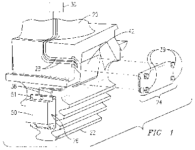
With reference to FIG. 1, embodiments of the present invention allow for
transmitting sensor data from a rotating component, such as a turbine engine
blade 20
having certain electronic components located on root 22 of the blade, which
operates in
an environment having a temperature exceeding 300 C. For purposes of the
disclosure herein, the term "high temperature" without additional
qualification will refer
to any operating environment, such as that within portions of a combustion
turbine,
having a maximum operating temperature exceeding 300 C.
Embodiments of the present invention provide components for use in a
combustion turbine instrumented with telemetry systems that may include one or
more
sensors, lead lines connecting sensors with at least one telemetry transmitter
circuit, at
least one transmitting antenna, a power source and at least one receiving
antenna.
CA 02878073 2014-12-23
WO 2014/004055 PCT/US2013/044888
6
FIG. 1 illustrates the turbine blade 20, a wireless telemetry transmitter
assembly 24 and
a rotating antenna assembly 26. Lead lines or connectors 28 may extend from
one or
more sensors, such as sensor 30, to telemetry transmitter assembly 24 when
mounted
proximate blade root 22. Lead lines 28 may route electronic data signals from
the
sensor 30 to telemetry transmitter assembly 24 where the signals are processed
by a
telemetry transmitter circuit formed on a circuit board contained within an
electronics
package 34 shown in FIG. 2. Lead lines or electrical connectors 36 may be
deposited
for routing electronic data signals from a telemetry transmitter circuit to
the rotating
antenna assembly 26.
FIG. 2 illustrates a high temperature electronics package 34 that may contain
a
high temperature circuit board and form part of telemetry transmitter assembly
24. The
main body of electronics package 34 may be fabricated from alloys with low
thermal
expansion coefficient such as Kovar brand alloy, an alloy of Fe-Ni-Co. The
thermal
expansion coefficient of Kovar alloy ranges from about 4.5-6.5x10⁻⁶ 1 C,
depending on
exact composition. The Ni-based alloys typically used for high temperature
turbine
components, such as turbine blade 20 have thermal expansion coefficients in
the range
of about 15.9-16.4x10⁻⁶ 1 C. Electronics package 34 may be affixed securely in
place
while allowing for relative movement between electronics package 34 and
turbine blade
20, as described below with respect to FIG. 2. This relative movement may
result from
their different thermal expansion rates, which occur over time during the high
number of
thermal cycles between ambient air temperature and the greater than 300 C
operating
temperature typically experienced proximate blade root 22.
The telemetry transmitter assembly 24, as best shown in FIG. 2, may include a
mounting bracket 37 and a lid or cover plate 38 with electronics package 34
positioned
there between. A plurality of connecting pins 40 enable connection between an
electronic circuit board contained within package 34, such as one having a
wireless
telemetry circuit fabricated thereon, and various external devices such as
lead lines
from sensors, induction coil assemblies or data transmission antennae.
Mounting
bracket 37, cover plate 38 and retention screws 39 connecting them together
(shown in
FIG. 1) may all be fabricated from the same material as is turbine blade 20.
This
ensures there is no difference in thermal expansion between turbine blade 20
and
CA 02878073 2014-12-23
WO 2014/004055 PCT/US2013/044888
7
mounting bracket 37. Consequently, no stresses are generated in mounting
bracket 37
or turbine blade 20 during thermal transients.
The thermal expansion coefficient of electronics package 34 may be different
than that of mounting bracket 37. When the operating system within which these
components reside is at a high temperature, electronics package 34, including
any
circuit board contained therein, that are formed of Kovar alloy would expand
less than
mounting bracket 37, which may lead to damage caused by vibrational energy in
the
system. In order to secure electronics package 34 within mounting bracket 37
to
accommodate the dimensional change differential between bracket 37 and
electronics
package 34, a layer of ceramic fiber woven fabric 41 may be placed between the
electronic package 34 and the inside surface of mounting bracket 37. Fabric 41
may be
fabricated from suitable ceramic fiber, including such fibers as silicon
carbide, silicon
nitride or aluminum oxide. For example, a quantity of Nextel TM aluminum oxide
based
fabric, manufactured by 3M, may be used for fabric 41.
With electronics package 34 and ceramic fiber woven fabric 41 assembled with
mounting bracket 37 and cover plate 38 to form telemetry transmitter assembly
24,
mounting bracket 37 may be attached to turbine blade 20 by a suitable means
for
attaching such as bolting, welding, brazing or via transient liquid phase
bonding. FIG. 1
illustrates a recess or flat pocket 42 that may be milled or otherwise formed
within
turbine blade 20 proximate blade root 22 for receiving assembly 24.
Cover plate 38 may be formed with a flange 44 oriented perpendicular to the
direction of G-forces, to add structural support to the cover plate, which
counters the g-
load forces occurring when rotating turbine blade 20 is operating at full
speed. This
relieves retention screws 39 from carrying the load applied to cover plate 38
via g-
forces, and allows them to be made sufficiently small so that the telemetry
transmitter
assembly 24 fits in the relatively small recess 42 with no interference with
any adjacent
components. If retention screws 39 were required to carry the load applied by
the G-
forces, their required size would be too large to fit in the available space.
FIG. 1 shows that the rotating antenna assembly 26 may be affixed to the end
face or neck of root 22. Assembly 26 may be an electronic assembly having
thermal
expansion coefficients different than those of the Ni-based alloys used for
turbine hot
gas path components such as turbine blade 20 including its root 22. One or
more
CA 02878073 2014-12-23
WO 2014/004055 PCT/US2013/044888
8
rotating antenna assemblies 26 may be protected from windage during rotation
of
turbine blade 20 at or near the speed of sound. In an embodiment, the windage
protection material is transparent to RF radiation frequencies in order to
enable
transmission of power and data through the material. Embodiments of rotatable
antenna assembly 26 may include a durable, protective, RF transparent cover 50
shown in FIG. 1, which is essentially a hollow fixture within which a data
antenna and
induction power components are contained. RF transparent cover 50 protects its
contents from the physical effects of windage during operation of the
combustion
turbine. Certain ceramics are suitable for protecting RF transmission
equipment from
the elements at elevated temperatures. However, many ceramics and ceramic
matrix
composites are prone to chipping and cracking under the vibrational impact and
G-
loading that a rotating turbine blade 20 experiences during operation of the
combustion
turbine. The inventors of the present invention have determined that RF
transparent
cover 50 may be fabricated from an RF transparent, high toughness, structural
ceramic
material. Ceramic matrix composites may be used to fabricate cover 50 as well
as
material selected from a family of materials known as toughened ceramics.
Materials
such as silicon carbide, silicon nitride, zirconia and alumina are available
with increased
toughness due to doping with additional elements or designed microstructures
resulting
from specific processing approaches.
One such material that is RF transparent, easy to form, and relatively
inexpensive is a material selected from a ceramic family generally referred to
as
zirconia-toughened alumina (ZTA). Ceramic material selected from this family
of
aluminum oxide materials is considerably higher in strength and toughness than
conventional pure aluminum oxide materials. This results from the stress-
induced
transformation toughening achieved by incorporating fine zirconium oxide
particles
uniformly throughout the aluminum oxide. Typical zirconium oxide content is
between
10% and 20%. As a result, ZTA offers increased component life and performance
relative to conventional pure aluminum oxide materials.
The designed microstructure of ZTA is fracture-resistant when the ceramic is
loaded in compression. However, if loaded sufficiently in tension, the ceramic
will fail
catastrophically, as with traditional ceramic materials. Consequently, RF
transparent
cover 50 is designed so that the tensile stresses in the ceramic material are
minimized
CA 02878073 2014-12-23
WO 2014/004055 PCT/US2013/044888
9
during operation of the combustion turbine. This is accomplished by designing
and
fabricating such that (1) all corners, edges and bends of the ZTA components
are
machined to eliminate sharp corners and edges, in order to reduce the stress
concentration factor at these locations, and (2) the orientation and fit of
the ZTA
component in a rotating antennae mounting bracket 51 is such that during
operation the
G-forces applied to the ZTA box do not generate significant bending stresses
in the
attachment flanges. This is accomplished by orienting the flanges parallel
with the G-
loading direction, rather than perpendicular to the G-loading direction, so
the ZTA flange
is loaded in compression and not in bending.
Mounting bracket 51 may be designed so that all the G-loading experienced by
rotating antenna assembly 26 during operation of the combustion turbine is
absorbed in
a direction extending toward the upper end of the bracket 51. No portion of
the
mounting bracket 51 extends far enough past an antenna contained therein to
attenuate
the RF transmission data signal. RF transparent cover 50 is secured in place
so its
internal stress field is primarily compressive and may be retained using
threaded pins
(not shown) through semicircular divots on its flanges.
Mounting bracket 51 may be attached to a face of the turbine blade 22 via
conventional means such as welding, brazing, bonding, bolting or screwing. An
embodiment of rotating antenna assembly 26 may be assembled by placing desired
antennae into the hollow body of cover 50 containing the antennae with a
ceramic
potting material. The potted RF transparent cover 50 containing the antennae
may then
be slid into mounting bracket 51, which may have been previously affixed to
turbine
blade root 22. Cover 50 may be secured to the mounting bracket 51 via pins
inserted in
the mounting bracket 51 and divots in the cover 50.
Referring now to FIG. 3 an exploded view showing the elements within the high
temperature electronics package 34 included within the housing 24 of FIG. 2,
is shown.
Package bottom cavity 34A includes electrical connecting pins 40 extending
from an
end thereof, which connectors enable communication between the electronics
inside
the package 34 and external sensors, sources and antennae. In order to
function at
high temperatures up to at least 450 C, the package must be designed and
sized to
contain the electronic circuit and its substrate, hereinafter PC board 42. The
package
must be able to withstand the temperature and centrifugal loading requirements
and
CA 02878073 2014-12-23
WO 2014/004055 PCT/US2013/044888
protect the circuitry on the substrate. Hence, the package 34 is made of gold-
plated
Kovar alloy and the electrical connecting pins 40 are made of gold. The gold
plating
on the package 34 prevents oxidation of the Kovar alloy, which can occur at
elevated
temperatures. The connectors 40 are insulated from the package by means of
individual insulating sleeves (not shown). A pair of the pins 40 is coupled to
electrical
connectors 28, which communicate with the sensor 30. A third pin is coupled to
ground
potential (electrical ground), while pins 4, 5, 6 and 7 are coupled to a
source of power
(two each for positive and negative ac). The last pin is used for coupling the
transmitter
output (data) signal to the antenna 26.
PC Boards
The PC board 42 or substrate is preferably fabricated from material capable of
operation at high temperatures, e.g., ceramic materials, such as alumina,
zirconia,
silicon carbide, silicon nitride, aluminum nitride, etc. The circuit runs (or
"printed
circuits") are preferably fabricated from metals that work at high
temperature, such as
silver, gold, platinum or palladium. The inventors chose a thick film process
using
alumina substrates for fabricating one embodiment of the PC board 42. The
alumina
substrates are metalized with a thick film gold paste. These substrates
performed very
well at high temperatures and were very compatible with the die attach process
(discussed below). Dupont QG150 brand gold paste was chosen as the
metallization.
This paste comprises a high-density gold powder with a glass oxide binder. The
PC
board may be formed of alumina of 10-100 mils thickness. The final substrates
comprise 96% alumina substrates measuring 20 mils thick. High density gold
paste
was used as the conductive layer, and also served as a surface capable of
being
soldered and wire bonded thereto. Printing capabilities allowed a line
resolution of 5
mils.
The PC board 42 is assembled by the following process as outlined hereinabove.
The substrates are prepared utilizing a thick film screen printing process. A
specialized
screen printer is used in conjunction with a patterned stainless steel fine
mesh screen.
The gold paste is printed onto an alumina (A1203) substrate. After printing,
the paste is
dried in an oven at 100 C to "bake out" the solvents in the paste. Next, the
substrates
are placed in a furnace and fired at 850 C. During this process, the
glass/oxide
binders in the paste form a strong bond between the sintered paste and the
alumina
CA 02878073 2014-12-23
WO 2014/004055 PCT/US2013/044888
11
substrate. Multiple prints require multiple firing steps. In accordance with
one
embodiment, two printing/firing cycles (top and bottom side metallization) are
employed.
Fired substrates are then cut out to the proper dimensions with a dicing saw.
The top print has the circuit pattern formed thereon, while the bottom print
is a metal
plane that has been "meshed" due to printability limitations. The back metal
plane will
allow metallurgical bonding processes to be performed thereon.
Once the PC board 42 is completed and components attached thereto
(described hereinafter), the PC board is then placed into the cavity 34A and a
12-carat
gold wire 44A, 44B is laser welded to the cavity for forming a retainer to
secure the PC
board in place via compression. Holding the substrate into the package
mechanically is
of utmost importance because of the high g-forces exerted on the package and
its
contents. The retainer may be formed of a material having a coefficient of
thermal
expansion within 20% of that of the package in order to minimize differential
thermal
growth there between. It is feasible to add a filler material into the package
34 and to
spread it over the PC board and the circuit components to help stabilize their
placement
during operation. However, any filler used must allow for any expansion or
contraction
of the components and their connecting wires during temperature cycles.
Finally, a lid
34B is secured to the top of the cavity 34A. In accordance with one
embodiment,
Kapton brand polyimide insulating tape was used to hold the lid 34B in place
until it
could be mechanically secured by compression. Another embodiment for securing
the
lid 34B is to weld it to the package cavity 34A.
As will be described in greater detail below, two different circuit layout
patterns
for the PC boards 42 may be used. A first pattern is designed for a circuit
that senses
changes of temperature of a selected component of the turbine, wherein the
sensor 30
is a thermocouple. The signal indicative of the component temperature is
amplified and
processed by the circuitry, then transmitted via an FM transmitter and
broadcast via an
antenna such as the antenna 26. This type of circuit may be used for sensors
other
than those measuring temperature, but that also produce a direct-current (D/C)
output
signal as a response, such as static strain, conductive trace, chemical
sensors or
pressure sensors. A second pattern is designed for a circuit that senses
dynamic strain
occurring on a selected component of the turbine, wherein the sensor 30 is a
strain
gauge. The signal indicative of the dynamic strain occurring on the selected
component
CA 02878073 2014-12-23
WO 2014/004055 PCT/US2013/044888
12
is amplified and processed by the circuitry, then transmitted via a separate
FM
transmitter and broadcast via an antenna such as antenna 26. This type of
circuit may
be used for sensors other than those measuring dynamic strain, but that also
produce
an alternating-current (NC) output signal as a response, such as
accelerometers or
electromagnetic wave emission detectors. An alternate embodiment uses a single
FM
transmitter that multiplexes multiple signals for transmission to a single FM
receiver
configured to decode the received signal into the two separate data signals.
The PC
board 42, as shown in FIG. 3, is partially complete in the illustration and is
generally
representative of the thermocouple circuit. Both circuits include an air core
inductor coil
L1, which is part of the tank circuit for the Colpitts oscillator of the FM
transmitter, which
will be explained further herein below. The quality factor Q of the coil L1
may be at
least 5 at the operating temperature and operating frequency of the circuit.
Sputtered
gold or silver material may be used to form the coil; however, such deposition
processes typically result in an inductor with a low Q value. The present
inventors have
successfully utilized gold or silver wire to form the inductor coil. The metal
wire air core
conductor may be potted along its length to prevent electrical shorts at high
frequencies. Insulating tape may be wrapped on the potted wire where it
crosses itself
so as to prevent electrical shorts. Alternatively, the metal wire may be
formed into a
bridge at cross over points thereof in order to prevent electrical shorts. In
order to
increase the mechanical strength and stability of such a coil, a potting
material may be
placed around the wire, although any such potting material will necessarily
affect the Q
factor of the coil. In one embodiment, gold wire potted with a ceramic alumina
paste
suspension (such as Ceramabond brand ceramic cement) provided a desired
degree
of structural stability at gas turbine operating temperatures and G forces and
provided a
Q factor of greater than 5. Such an alumina-based potting also acts as an
electrical
insulator for the coil, so no separate electrical insulation is required
around the wire
itself.
Die/Component Attachment
In order for the electronic package to function at elevated temperatures up to
at
least 450 C and to withstand centrifugal loading greater than 1000 g's,
special
requirements are to be met for attaching components to the PC board 42. All
bonds are
performed in a vacuum oven for assurance of proper reflow of the solder. The
inventors
CA 02878073 2014-12-23
WO 2014/004055 PCT/US2013/044888
13
have appreciated a major problem that may be encountered when the component
being
soldered has a trivial mass. If the mass of the component is very small, it
may be
unable to break the surface tension of the liquid alloy as it beads up, and
the
component part may be pushed off the solder and slide to another position, or
it may tilt
at an angle (called "tomb stoning").
To overcome this problem, the present inventors have developed an approach
utilizing a transfer plate and component alignment templates that fit in the
heated fixture
of the vacuum oven. A transfer plate 60 is shown in plan and elevation views
in FIG. 4A
and a pair of component alignment plates 61 and 62 are shown in FIG. 4B, also
in plan
view. FIG. 4A illustrates plan and end views of the transfer plate 60 used in
assembling
the PC board 42 shown in FIG. 3. The plate is made of graphite and is sized
and
shaped for receipt of the substrate (PC board) and the alignment plates 60, 61
for
aligning the components to be attached to the PC board during the assembly
operation.
The alignment plates 60, 61 must be capable of withstanding high-temperatures,
must
be inert and resistant to solder, and must be capable of defining highly
precise cutouts
for the components. Accordingly, alloy 316 stainless steel may be used to
fabricate
these plates. Due to the small size of the cutouts and the need for high
precision, laser
cutting may be used for fabrication.
The next concern is the formulation of the solder for attaching the components
to
the PC board 42. The material must be compatible with the die metallization
(Au thin
film) and the substrate metallization (Au thick film).
Brazing, which is a relatively straightforward process involving the melting
of a
high temperature filler metal in between two wetting surfaces, was found to be
less than
optimal for the present application due to three primary factors: (1) most
brazes have a
liquidus temperature over 700 C and require highly corrosive fluxes; (2) many
brazing
alloys are not eutectic and have a very large plastic region which may
complicate
processing; and, (3) most brazes are not compatible with gold surfaces.
The inventors also found Transient Liquid Phase (TLP) bonding to be less than
optimal. In this process, a low melting point alloy is liquefied between two
compatible
surfaces. As the alloy fills in the gaps between the faying surfaces, it acts
to "dissolve"
or "leach" away compatible metals. This action changes the composition of the
alloy,
thereby shifting the melting point of the filler, resulting in solidification
and an extremely
CA 02878073 2014-12-23
WO 2014/004055 PCT/US2013/044888
14
high quality bond. The primary requirement of this process is that the
surfaces being
bonded to are thick while the molten alloy layer is extremely thin. When this
process
was applied to plated thin film (20 microns thick) and thick film (25 microns
thick)
substrates, the inventors found a very large inconsistency in the results with
many not
passing acceptance requirements.
The inventors have discovered that a solid state diffusion process utilizing
pure
gold is useful for the present application. In this process, no liquid metal
is utilized.
Instead, the rapid self diffusion property of gold is used to create a very
high quality
bond between two pure gold surfaces. While solid state diffusion may be
performed
with no filler material, it typically requires very high pressures to compress
the facing
surfaces together to obtain suitable contact area. In lieu of such pressure,
the inventors
selected a gold filler material to fill in the gaps between the bonding
surfaces. Both gold
foil and powder were investigated, with powder proving to be the better
option, due to its
ability to both fill in the gaps and to form a solid, homogeneous layer under
heating due
to sintering. Sintering is a process utilizing diffusion to join two small
particles together
into a solid matrix. This is generally performed at elevated temperature to
increase the
rate of diffusion. While the solid state diffusion process may be performed
with a gold
powder, it was further discovered that a gold paste was easier to use in this
application.
A paste may be applied by a number of methods, including dispensing, stamping,
and
screen printing. The major difference between a gold paste and a gold powder
is that
the paste has both an organic vehicle (such as polymers, terpineol, or glycol
ethers)
which acts as a transfer medium so that the powder may be easily applied, and
surfactants that act to separate the powders until bonding is desired.
A number of gold thick film pastes were selected for use. While the paste has
other additives (oxide based binders and glass frits) which will provide no
adhesion to a
pure gold layer, they are compatible with alumina substrates and thick film
gold
metallization. Additionally, these pastes are readily available, contain small
high purity
gold powder, and are designed for easy application. While many gold pastes
have
proved compatible, the best performing option was found to be DuPont QG 150,
which
is the paste with the highest gold composition available. This is the same
paste used to
metalize the substrate, and thus is very compatible with the entire system. In
this
process, the die and components are placed upon the gold metalized substrate
with a
CA 02878073 2014-12-23
WO 2014/004055 PCT/US2013/044888
small amount of the QG 150 gold paste. The assembly is then placed in an oven
at 400
C for 12 hours. During this time, the gold-gold diffusion takes place between
neighboring gold particles and between the particles and the bonding surfaces.
The
resulting bond is very strong and capable of withstanding temperatures well
above 500
C. Additionally, the process is straightforward, fast, repeatable, and may be
performed
on very small components.
Referring now to FIGS. 5A, 5B and 5C, perspective views of the transfer plates
used for aligning and assembling the components on the circuit board are
shown. First,
the substrates or PC boards 42 are placed in the cavities of the transfer
plate 60. Next,
the alignment plates 61, 62 are placed over the substrates. The component
attachment
gold paste is then placed in the openings of the alignment plates and the
components
are then placed in the openings of the alignment plates 60, 61 for the
assembly
operation. The transfer plate 60 along with the substrates, alignment plates,
gold paste
and components are sandwiched between heated graphite plates 65, as shown in
FIG.
5C. The assembly is next placed in an oven at 400 C for 12 hours. During this
time,
gold to gold diffusion takes place, and the die and components remain attached
with a
high shear strength at temperatures greater than 500 C. The process is made
repeatable by a pick-and-place machine that properly aligns the die and
components.
Wire Bonding
Wire bonds are the standard method used in many electronic applications;
however, they are not known by the inventors to be employed in an environment
that
subjects them to such high sheer forces (i.e., g-loading) while at high
temperatures.
Referring now to FIGS. 6A and 6B, wire bonding techniques typically used in
the
semiconductor arts are shown. FIG. 6A illustrates the foot and heel of each
end of the
bonding wire, and FIG. 6B illustrates the terms "loop height" and "bond
length". FIG. 7
is a perspective view showing g-force analysis of a typical wire bonding,
wherein the g
forces are applied from four different directions. First, there are two
possible forces in
opposite directions across the wire bond (i.e. in directions parallel to the
wire) that are
labeled as the X and -X direction, and then there are two possible forces in
opposite
directions into the wire bond (i.e. in directions perpendicular to the wire)
that are labeled
as the Z and -Z direction. FIG. 8 illustrates diagrams of the wire bonding
showing
deformation of the wire under simulated g-force stress in these various
directions. The
CA 02878073 2014-12-23
WO 2014/004055 PCT/US2013/044888
16
interconnect technology used to connect integrated circuits to a PC board is a
critical
component to any electronic system.
Under high g-forces, it is normally expected that the wire bonds would deflect
to
a certain degree from their original position. The present inventors have
unexpectedly
discovered that it is possible to utilize gold wire bonds in the high
temperature and high
g environment of the present invention. It was found that loading of the wire
bond in the
X direction (Load Set 2 in FIG. 8) resulted in the least overall stresses in
the wire. Gold
wire bonds of both 0.7 and 1.0 mil diameter have been used. It has been shown
that
both diameters of wire bonds will be structurally stable if they are oriented
parallel to the
centrifugal loading, the maximum loop height is no greater than 17.4 mil, and
the
maximum bonding length (from bonding pad to bonding pad) is kept under 35 mil.
These results are acceptable for loadings of greater than 1,000 g's, and in
fact, were
tested to be acceptable to loadings over 10,000 g's. The wire properties, loop
height,
bonding length and temperature all affect the maximum sustainable G-load of
the wire
bond.
Electronics
Referring now to FIG. 9A, an exemplary schematic diagram is shown that
illustrates the unique circuit biasing for amplifier circuits used herein. The
function of
the bias circuit is to place the JFET's into the proper area of operation. For
a JFET, the
places of operation can be various points within the ohmic region, where the
JFET
behaves as a small resistor, or within the saturation region, where the JFET
behaves as
a voltage controlled current source. Different biasing points lead to
different JFET
behavior; even different points within the same region. Many of the JFET's
characteristics change when the JFET is operated over the temperature range of
25 C
to 500 C. Of specific interest herein is the fact that the device is going to
exhibit less
gain at high temperature than at low temperature. Another important change is
the
characteristics of the JFET performance over temperature, which is the
downward
(more negative) shift of the JFET threshold voltage over increasing
temperature, which
is demonstrated in the diagram of FIG. 96.
Structurally, the amplifier circuit shown in FIG. 9A includes a voltage
divider
network comprising RI3_1 and R6_2 serially coupled between a source of
positive
voltage V(+) and source of negative voltage V(-). A circuit node 1000
connecting RI3_1
CA 02878073 2014-12-23
WO 2014/004055 PCT/US2013/044888
17
to R6_2 is coupled to one side of an input capacitor C_1 and to the gate
terminal of a
JFET Ql. The other side of C_1 is coupled to the input terminal V(in). The
source
terminal of the JFET Q1 is coupled to ground potential, and the drain terminal
thereof is
coupled to one side of a load resistor RD. The other side of the resistor RD
is coupled
to the source of positive voltage V(+). The drain terminal of Q1 is also
coupled to the
output terminal V(out) through another capacitor C_2.
FIG. 96 illustrates the changing level of AC output voltage versus bias
voltage of
the amplifier of FIG. 9A under varying temperatures. That is, the level of
voltage on the
node 1000 is plotted on the horizontal axis of FIG. 96, and the resulting
output voltage
V(out) is plotted on the vertical axis. Curve 1001 represents the output
voltage at a
temperature of 25 C; curve 1002 represents the output voltage at 100 C;
curve 1003
represents the output voltage at a temperature of 200 C; curve 1004
represents the
output voltage at a temperature of 300 C; curve 1005 represents the output
voltage at
a temperature of 400 C; and, curve 1006 represents the output voltage at a
temperature of 500 C.
In a JFET common source ac amplifier (e.g., FIG. 9A), there is a narrow range
of
bias voltage that results in the highest ac voltage gain. Accordingly, as may
be seen
from this figure, there is a decreased gain over temperature that results in a
lower
maximum ac output voltage. Also, it is shown that the bias point where the
maximum
peak-to-peak output voltage occurs shifts to the left (more negative dc gate
bias voltage
with increased temperature). The ideal biasing circuit will track the peak
thereby
providing optimal performance. Hence, it is desirable to adapt the biasing dc
voltage
with temperature changes.
The resistors RI3_1 and R6_2 set the dc operating point of the gate to source
voltage (Vgs) of the common source amplifier (FIG.9A), which is the same
voltage as
that depicted on the horizontal axis of FIG. 96. For example, the bias point
for the
peak ac voltage output at 25 C is where Vgs = -1.7v. The resistor RD is the
JFET
drain resistor, which helps determine the voltage gain of the amplifier. Two
characteristics that must be accounted for when biasing the circuit over the
temperature
excursion (of 25 C to 450 C) are the bias point set by resistors RI3_1 and
RI3_2, which
should track the voltage results in the peak output voltage; and, the gain of
the circuit
should be increased with increasing temperature. If the above two measures are
taken,
CA 02878073 2014-12-23
WO 2014/004055 PCT/US2013/044888
18
the output characteristics of the device will remain essentially constant over
the
temperature range of interest. This can be accomplished by designing the
resistor
RB _1 to have a positive temperature coefficient (PTC) of resistance, while
the resistor
RB _2 has a zero temperature coefficient (ZTC) of resistance. A second
approach is to
give the resistor RD a PTC as well, so as to increase the amplifier gain as
the
temperature increases (resulting in a gain at high temperature equal to that
at low
temperature).
Temperature coefficients of resistance can be implemented in several ways.
They can potentially be applied using surface mount thermistors or they can be
fabricated with different materials affixed to the circuit board. There are
many thick film
pastes available that possess various temperature coefficient of resistance
(TCR). In
accordance with one embodiment, the resistors RB_1 and RD are formed of TaN
Thick
Film, while the resistor RB_2 is formed of Platinum Thick Film.
Referring now to FIG. 10, a block diagram of the strain gauge circuit is
shown. A
signal indicative of the amount of strain placed on a measured turbine
component is
produced by a strain gauge 101. This signal is then sensed by a differential
amplifier
102 and coupled to an AC amplifier 103 for further amplification. The
amplified strain
gauge signal is then applied to the input of a voltage controlled oscillator
104, which
produces an oscillatory signal the frequency of which is representative of the
strain
placed on the measured turbine component. This oscillatory signal is then
buffered by
a buffer 105 and passed on to the antenna 26 for transmission to a
conventional tuner
(not shown) tuned to the carrier frequency.
Referring now to FIG. 11, a block diagram of the thermocouple circuit is
shown.
A signal indicative of the temperature of a measured turbine component is
detected by
a thermocouple 110, which signal is passed on to a differential amplifier 111.
The
output of the differential amplifier 111 is passed on to a dc amplifier 112.
The output of
the amplifier 112 and the output of a square wave oscillator 113 (or square
wave
generator) are coupled to inputs of a "chopper" 114. The output of the chopper
114 is
coupled to the input of a voltage controlled oscillator 115, which produces an
oscillatory
signal the frequency and amplitude of which is representative of the
temperature
sensed on the measured turbine component. This oscillatory signal is then
buffered by
a buffer 116 and passed on to the antenna 26 for transmission to a
conventional tuner
CA 02878073 2014-12-23
WO 2014/004055 PCT/US2013/044888
19
(not shown) tuned to the carrier frequency. Where both types of circuits are
used on
the same turbine, the carrier frequencies would be different in order to avoid
confusion
between the two signals.
Referring now to FIG. 12, a schematic diagram of the circuits 101, 102, and
103
for amplifying a strain gauge output signal is shown. Modification of the
traditional
wireless telemetry circuit design was required in order to accomplish the
required tasks
electrically with a more limited selection of available electrical devices
usable at
temperatures in excess of 450 C. A strain Gauge signal conditioning
(excitation and
amplification) circuit was designed using only one type of transistor, a JFET
with high
temperature metallization. The connection of the metal bonding pads (i.e.,
gold) cannot
be made directly to the semiconductor material, but must utilize an adhesion
layer, such
as Tungsten, and perhaps adding a diffusion barrier as well. These metals
comprise
the "metal stack" of the die, i.e., high temperature metallization.
Structurally, there is a voltage divider network comprising resistor R7 and a
Strain Gauge coupled between a source of positive voltage Vdc(+) and ground
potential. Circuit node 1100 is the connection point between resistor R7 and
the Strain
Gauge, and is also coupled through a capacitor C4 to the gate terminal of a
JFET
transistor J1. The transistor J1 is biased by a pair of resistors RI3_1 and
R6_2, which
are joined at the gate terminal of this transistor, in the same manner as
described above
with reference to FIG. 9A. Transistor J1 is half of a differential amplifier
that includes
transistor J2. The drain terminal of the transistor J1 is coupled to the
positive voltage
Vdc(+) through a resistor R1 and the drain terminal of the transistor J2 is
coupled to the
same Vdc(+) through a resistor R2. The source terminals of the transistors J1
and J2
are coupled together and to the drain terminal of another transistor J3, which
includes a
gate terminal coupled to ground potential and the source terminal thereof
coupled also
to ground potential through another resistor R3. The gate terminal of the
transistor J2 is
also coupled to ground potential. Therefore, any change on the gate terminal
of the
transistor J1 will be amplified at the drain terminal thereof and coupled
through a
capacitor C1 to the gate terminal of yet another transistor J4, which is the
first of three
more stages of amplification (ac amplifier 103) including transistors J5 and
J6, with the
output of the amplifier provided at a terminal Vout.
CA 02878073 2014-12-23
WO 2014/004055 PCT/US2013/044888
A change in the strain placed on the component being measured, which
component includes the Strain Gauge, changes the resistance of the Strain
Gauge
resistor, thereby changing the voltage at the gate terminal of the transistor
J1. This
changes the output of the transistor J1 across a resistor R1, which is coupled
to
succeeding stages of amplification by the transistors J4, J5 and J6. All of
the resistors
shown in FIG. 13, with the exception of the resistor RI3_1 (which has a PTC),
have a
very low (close to zero, slightly positive) temperature coefficient of
resistance. Also, all
of the JFET transistors are made with high temperature metallization, as
described
hereinabove.
Referring now to FIG. 13, a schematic diagram of the circuits 110, 111 and 112
for amplifying a thermocouple output and embedding the local temperature of
the
thermocouple circuitry into the amplified output signal is shown. In this
manner, the
thermal gradient across the thermocouple, rather than just the thermocouple
output, can
be transmitted, thus giving an accurate temperature measurement. FIG. 16
illustrates
the thermocouple 110 coupled to the circuitry shown in the block diagram of
FIG. 11
(i.e., the thermocouple circuitry 201). The thermocouple 110 output is shown
as
representing AT C. As will be shown and described further hereinafter it is
the sum of
AT C and the local temperature of the thermocouple circuitry 201 that
represents the
true measured temperature of the turbine.
Referring again to FIG. 13, the negative leg of the thermocouple is grounded,
and the positive leg is connected to the gate terminal of a transistor J7,
which along with
transistor J8, forms the differential amplifier 111. This differential
amplifier is biased by
the voltage divider comprising RI3_1 and R6_2 coupled together at the gate
terminal of
transistor J7 plus a current source formed with a transistor J9. As described
hereinabove, the resistors RI3_1 has a PTC and the resistor R6_2 has a ZTC in
order
to compensate for the high temperature environment (see FIG. 9A and
accompanying
description).
Since the thermocouple signal is dc, or very low frequency ac, successive
amplification stages cannot be capacitively coupled. Instead, a transistor J10
is used in
the source follower configuration to shift the output of the differential
amplifier down to
the level at which the common source transistor J11 must be biased. It will be
appreciated that the source follower lowers the output impedance of the
differential
CA 02878073 2014-12-23
WO 2014/004055 PCT/US2013/044888
21
amplifier. The transistor J11 serves to further amplify the signal.
Transistors J12 and
J14 form another level shifting and amplification stage (dc amplifier 112). At
this point,
the output of the thermocouple has been amplified to an appropriate level. Now
the
local temperature of the thermocouple circuitry must be embedded into the
amplified
signal.
Transistors J14 and J15 form a differential pair amplifier, biased by a
current
source formed by a transistor J16. Capacitors C6 and C7, along with resistors
R18,
R19 and R20 form a -90 to +90 phase shift network. This phase shift network
is
connected at one end of the amplifier input at the transistor J15, and the
other end is
coupled to the output of the amplifier (the drain terminal of the transistor
J14), which
comprises an RC feedback network. This configuration forms a relaxation type
RC
oscillator (square wave oscillator 113). Capacitors C6 and C7 are NPO type
capacitors,
and their capacitance does not change appreciably over the temperature
excursion of
25 C to 450 C. An NPO capacitor dielectric has a negative-positive¨zero
temperature
coefficient of capacitance, wherein the positive and negative temperature
coefficients
cancel one another out. Capacitor C8 is coupled in series between the RC
feedback
network and the output of the differential amplifier at the drain terminal of
transistor J14.
This capacitor is made with an X7R dielectric, and thus its capacitance
changes
predictably with temperature changes. X7R is a capacitor dielectric that has a
higher
dielectric constant than does the NPO dielectric, but has a large capacitance
dependence on temperature (which is predictable). The output of this
oscillator is a
square wave with a frequency determined by the temperature dependent capacitor
C8;
thus, the local temperature of the thermocouple circuitry may be encoded into
the
square wave signal. (See the oscillator 113 output waveform 210 shown in FIG.
17 at
room temperature; and the same oscillator output waveform 212 at an elevated
temperature, shown in FIG. 18). A transistor J27 serves as a chopper
transistor (i.e.,
chopper 114). The amplified thermocouple output from the transistor J13
(waveform
214 in FIG. 19) is coupled to the drain terminal of the transistor J27, while
the square
wave oscillator output is coupled to the gate terminal of the same transistor
J27. The
source of the transistor J27 provides a square wave output, whose amplitude is
proportional to the temperature of the thermocouple 110 and whose frequency is
proportional to the temperature of the thermocouple circuitry (see waveform
216 shown
CA 02878073 2014-12-23
WO 2014/004055 PCT/US2013/044888
22
in FIG. 20).. Thus, the signal contains the thermocouple output plus the
temperature of
the thermocouple circuitry, which signal is applied to the voltage controlled
oscillator
115.
By way of example of operation of the thermocouple 110 and its circuitry 113,
assume that the temperature of the circuitry 113 is at 25 C and the
corresponding
output of the oscillator 113 is at a frequency of 1.62 kHz (waveform 210, FIG.
17). Also,
assume for the particular thermocouple 110 being used that a 12 my output
voltage
(waveform 214, FIG. 19) corresponds to a AT of 320 C. Now, assume that the
temperature of the circuitry 113 is 325 C and the output of the oscillator
113 is 5.44
kHz (waveform 212, FIG. 18). By combining the waveforms 212 and 214 with the
transistor J27, the resultant output of the transistor J27 (i.e., output of
the circuit) is
illustrated by the waveform 216. Thus, the resulting temperature measured is
645 C at
the hot end of the thermocouple. The frequency of the waveform 216 represents
the
temperature of the local circuitry 113 and the amplitude represents AT.
Accordingly,
one skilled in the art can construct circuitry associated with the FM receiver
(not shown)
to perform signal decoding and addition operations.
Referring now to FIG. 14, a schematic diagram of the power conditioning
circuitry
is shown. A power conditioning circuit capable of rectifying an RF input
voltage, filtering
and rectified voltage, and regulating that voltage had to be designed using
only one
type of transistor and available diodes. The circuit rectifies RF induction
power
provided by the rotating turbine and delivers a positive and negative
regulated dc
voltage. Structurally, diodes D5 through D8, as well as diodes D9 through D11,
serve
as a bridge rectifier. An ac voltage on terminals Vac1 and Vac2 or Vac3 or
Vac4 is full-
wave rectified into a dc voltage with a large ripple. Capacitors C9 through
C12 serve as
filter capacitors in order to reduce the ripple to a sufficiently low level.
Transistors J17
and J21 serve as constant current sources, delivering a constant current into
resistors
R26 and R30, respectively. This constant current going through a constant
resistance
produces a constant voltage, which is coupled to transistors J19 and J23. This
constant
voltage biases transistors J19 and J23 such that, after a threshold determined
by the
R25/R26 resistor pair or R29/R30 resistor pair, any increasing voltage at the
inputs to
the transistors does not contribute to an increasing voltage at the transistor
outputs.
The increasing voltage input is dissipated as heat in the transistors J19 and
J23. Thus,
CA 02878073 2014-12-23
WO 2014/004055 PCT/US2013/044888
23
the transistors J17 and J19, as well as transistors J21 and J23 comprise low-
dropout
(LDO) voltage regulators. These regulators are repeated with the transistors
J18 and
J20, as well as the transistors J22 and J24 to improve the net voltage
regulation. The
voltages are then supplied as either positive or negative regulated voltages
Vdc(+) or
Vdc(-), respectively.
In accordance with one embodiment the resistors R26, R28, R30 and R32 have
a PTC, whereas the resistors R25, R27, R29 and R31 have a ZTC. As discussed
hereinabove, this arrangement of resistors compensates for changes in bias
voltages at
elevated temperatures. In this way the circuit self compensates for
temperature
variations and keeps the voltage drop across the transistors J19, J20, J23 and
J24
constant. As described hereinabove, PTC resistors may be made of platinum and
ZTC
resistors may be made of tantalum nitride. It is pointed out that the circuit
would also
function the same where the resistors R26, R28, R30 and R32 were made with ZTC
and the resistors R25, R27, R29 and R31 were made with a negative temperature
coefficient (NTC) by the use of a silicon resistor, such as silicon carbide.
Referring now to FIG. 15, a schematic diagram of the FM transmitter (i.e., VCO
104 and Buffer 105) is shown. In order to create a frequency modulated (FM)
signal, a
variable impedance device is commonly used to encode (i.e., modulate)
information
onto an RF carrier wave. A common way to do this task in low-temperature
circuitry is
to use a device whose capacitance has a dependence on applied voltage. Almost
all
pn junction diodes exhibit this characteristic when reverse biased; that is, a
varying
voltage applied to a reversed biased diode affects change in the capacitance
across the
diode. For low-temperature radio applications, a special diode, called a
varactor, is
used for this purpose. The varactor is a pn junction diode, with a "hyper-
abrupt"
junction (i.e., a junction that is heavily doped to promote a large tuning
angle) and is
fabricated from silicon or gallium arsenide.
The circuit shown in FIG. 15 includes a Colplitts oscillator comprising an
inductor
L1 and serially coupled capacitors 013 and 014, both of which are coupled in
parallel
with the inductor L1. A transistor J25 serves as the active device in the
Colplitts
oscillator. The carrier frequency of the oscillator is determined by the value
of the
inductor L1 and the capacitors 013 and 014. A diode D13, which is coupled in
parallel
with the capacitor 014, serves as a voltage variable capacitor, or varactor,
which
CA 02878073 2014-12-23
WO 2014/004055 PCT/US2013/044888
24
modulates (i.e., encodes) an ac voltage onto the carrier wave. The carrier
wave is then
capacitively coupled into a transistor J26, which serves as both a buffer
transistor as
well as a power amplifier. The cathode of the diode D13 is coupled to a
circuit node
1400 and the anode thereof is coupled to the ground potential. The circuit
junction
between the capacitors 013 and 014 is coupled to the node 1400, which also
comprises the input terminal V(in) to the circuit. The output of the circuit
is then
capacitively coupled into the transmit antenna (not shown).
In high-temperature applications, typical varactors cannot be used and are not
useful in the FM transmitter of interest herein because the capacitance of
such
varactors may not be consistently repeatable or predictable due to hysteresis
effects
non-linear over a range of applied bias voltages at elevated temperatures.
Hence,
correct information could not be recovered from the transmitted signal
(identical
frequency deviations would not correspond to distinct tuning voltages). It was
discovered that the problem was intrinsic to SiC itself, and thus no SiC
device would
achieve the desired result. GaN devices, which can function at high
temperatures (i.e.,
have a linear capacitance over the same range of applied bias voltages at the
same
elevated temperatures), were explored for use as the varactor diode D13.
Gallium
Nitride (i.e., GaN) is also a wide band gap semiconductor, with a wide band
gap energy
of 3.4 eV @ 300 K(whereas SiC is 2.86 eV), meaning that it can function at
high
temperature (in excess of 600 C). The only commercially available GaN diode
currently available is in the form of a blue or ultraviolet LED, which
produced
satisfactory results across the temperature excursion of interest herein.
The description below will provide details of circuitry embodying aspects of
the
present invention, which in one example application may be used in strain
gauge
circuitry, as exemplarily illustrated in FIG. 21. It will be appreciated that
such example
application should not be construed in a limiting sense being that circuitry
embodying
aspects of the present invention may be used in other applications.
FIG. 22 is a schematic representation of one example embodiment of circuitry
120 embodying aspects of the present invention. Circuitry 120 includes a
differential
amplifier 122 having an input terminal 124, which may be coupled to a sensing
element
(e.g., strain gauge 101 FIG. 21) to receive a voltage indicative of a sensed
parameter
(e.g., voltage indicative of strain). Differential amplifier 122 may include a
first pair of
CA 02878073 2014-12-23
WO 2014/004055 PCT/US2013/044888
semiconductor switches 126, 128 (e.g., differential pair of semiconductor
switches).
Biasing of the differential pair of semiconductor switches 126, 128 may be
controlled by
a respective bridge circuit (gate bias network) made up of resistors R5, R6,
R7 and R8,
which may optionally use the temperature-compensated biasing techniques
described
above in the context of FIGs. 9A and 9B. For example, as the temperature
increases, a
respective bias voltage at the respective gate terminals of the semiconductor
switches
126, 128 decreases. Circuitry 120 further includes a hybrid load circuitry
125, which in
accordance with example aspects of the present invention may be AC-coupled
(alternating current-coupled) to differential amplifier 122, as elaborated in
greater detail
below.
Hybrid load circuitry 125 may include a second pair of semiconductor switches
130,132 (e.g., active-load pair of semiconductor switches). Each of such pairs
of
semiconductor switches has a respective drain terminal (D), a respective
source
terminal (S) and a respective gating terminal (G). In one example embodiment,
the first
pair of semiconductor switches 126, 128 and the second pair of semiconductor
switches
130, 132 involve circuitry without complementary pairs of semiconductor
switches. In
one example embodiment, the first pair of semiconductor switches 126, 128 and
the
second pair of semiconductor switches 130,132 may be n-channel junction gate
field-
effect transistor (JFET) switches and may comprise a respective high-
temperature, wide
bandgap material, such as SiC, AIN, GaN, AlGaN, GaAs, GaP, InP, AlGaAs, AlGaP,
AlInGaP, and GaAsAIN.
As will be appreciated by one skilled in the art, p-channel SiC JFETs are
presently believed to be impractical due to their relatively low-channel
mobility, and
consequently, known active load topologies for differential amplifiers have
not been
utilized in high-temperature applications since such topologies would involve
p-channel
SiC JFETs. Hybrid load circuitry embodying aspects of the present invention,
advantageously eliminates a need of p-channel JFETs, and thus such a circuitry
can
reach the theoretical temperature limits of high-temperature, wide bandgap
material
JFETs (e.g., above 500 C) and effectively provide a high-gain differential
amplifier,
which, in one example application, may be utilized to appropriately amplify in
a high-
temperature environment the relatively low-voltage (e.g., a few millivolts)
electrical
CA 02878073 2014-12-23
WO 2014/004055 PCT/US2013/044888
26
signals, which may be generated by sensors, such as thermocouples and strain
gauges.
In one example embodiment, hybrid load circuitry 125 may further comprise a
resistor-capacitor circuit 134 (e.g., a resistor 142 and a capacitor 140)
arranged to
provide a path (e.g., relatively high-impedance path) to an AC signal
component with
respect to the drain terminal of the switch of the differential pair of
semiconductor
switches, which receives the voltage indicative of the sensed parameter (e.g.,
switch
126). Circuit 134 is connected to a node 136 coupled in parallel circuit to
the respective
gate terminals of the second pair of semiconductor switches 130,132. It will
be
appreciated that node 136, which is connected to an electrical ground 135 by
way of
resistor 142 is effective to maintain an appropriate biasing for semiconductor
switches
130, 132.
In one example embodiment, the value of resistor 142 may be chosen to be
sufficiently low relative to the value of the input impedance at the
respective gate
terminals of switches 130, 132 so that, for example, an AC signal component at
the
drain terminal of differential switch 126, would be AC-coupled by way of
capacitor 140
to the path provided by resistor 142, in lieu of the gate terminals of
switches 130, 132.
For example, presuming an input impedance in the order of 20 MO at the
respective
gate terminal of switch pair 130,132 relative to a resistance value in the
order of 2 MO
for resistor 142, it would be appreciated that resistor-capacitor circuit 134
would effect a
high-impedance path to such AC signal component (e.g., at the drain of
differential
switch 126), and this effectively increases the AC gain of the differential
amplifier.
For biasing purposes, hybrid load circuitry 125 may include a first resistor
144
coupled from a source terminal of one of the switches of the second pair of
semiconductor switches (e.g., switch 130) to a drain terminal of one of the
switches of
the first pair of semiconductor switches (e.g., differential switch 126).
Hybrid load
circuitry 125 may further include a second resistor 146 coupled from a source
terminal
of the other one of the switches (e.g., switch 132) of the second pair of
semiconductor
switches to a drain terminal of the other one of the switches of the first
pair of
semiconductor switches (e.g, differential switch 128). First and second
resistors 144
and 146 each may comprise a positive temperature coefficient of resistance so
that as
temperature varies the gain of the amplifier remains substantially constant.
That is,
CA 02878073 2014-12-23
WO 2014/004055 PCT/US2013/044888
27
constant other than applicable tolerances and deviations, as would be
understood by
one skilled in the art in the context of a practical, real-world device. A
node 148
connected to the source terminal of switch 132 provides the amplified
differential
amplifier output. Preliminary experimental results have demonstrated
feasibility of
differential gains of at least approximately 47.8 dB, 51.4 dB and 57.8 dB at
temperatures of 450 C, 300 C and 25 C, respectively.
FIG. 21 illustrates a block diagram of an example power source circuitry 239,
which may be used in a turbine component (e.g., turbine blade 20 (FIG. 1))
instrumented with a telemetry system. In one example embodiment, one or more
loads
may be electrically powered by power source circuitry 239. By way of example,
loads
may be electronic circuitry, such as sensing (e.g., strain gauge 101), signal
conditioning
(e.g., differential amplifier 102), and/or telemetry circuitry (e.g., voltage
controlled
oscillator 104, buffer 105), which may be part of the telemetry system.
Power source circuitry 239 may acquire electrical power by way of one or more
power-harvesting modalities, such as induced RF (radio frequency) energy
and/or by
harvesting thermal or vibrational power within the turbine engine. For
example,
thermopiles may be used to generate electricity from thermal energy, or
piezoelectric
materials may generate electricity from vibration of the turbine engine. For
readers
desirous of general background information regarding examples forms of power
harvesting modalities, reference is made to US patent No. 7,368,827, titled
"Electrical
Assembly For Monitoring Conditions In A Combustion Turbine Operating
Environment",
the entire disclosure of which is incorporated herein by reference.
Regardless of the specific power-harvesting modality, in one example
embodiment AC (alternating current) power 241 may be supplied to a rectifier
242,
which converts the AC input to a DC (direct current) output, which is coupled
to a
voltage regulator 244, which may be configured to maintain a relatively
constant DC
voltage output 245, even in the presence of variation of the harvested AC
input voltage.
It will be appreciated that a constant voltage output may be desired to
achieve a
required measurement accuracy and/or stability for any given engine parameter
being
measured.
FIGs. 23-24 and related description below will provide details of a voltage
regulator 250 embodying aspects of the present invention, which in one example
CA 02878073 2014-12-23
WO 2014/004055 PCT/US2013/044888
28
application, may be used in a power source circuitry, as exemplarily
illustrated in FIG.
21. It will be appreciated that such example application should not be
construed in a
limiting sense being that circuitry embodying aspects of the present invention
may be
used in other applications.
In one example embodiment, voltage regulator 250 may be adapted to operate in
a high-temperature environment of a turbine engine. Voltage regulator 250 may
include
a constant current source 252, such as may include a first semiconductor
switch 254
and a first resistor 256 connected between a gate terminal (G) and a source
terminal
(S) of first semiconductor switch 254.
In one example embodiment, a second resistor 258 may have a first lead 260
connected to the gate terminal (G) of first semiconductor switch 254 and a
second lead
262 connected through node 263 to an electrical ground 64. Constant current
source
252 may be coupled to generate a voltage reference (Vr) across second resistor
258. A
source follower output stage 266 may include a second semiconductor switch 268
and
a third resistor 270 connected between electrical ground 264 and a source
terminal (S)
of second semiconductor switch 268. As can be appreciate in FIG. 23, first
lead 260 of
second resistor 258 is connected to apply the generated voltage reference (Vr)
to a
gating terminal (G) of second semiconductor switch 268. It can be further
appreciated
that the source terminal (S) of second semiconductor switch 268 supplies a
regulated
output voltage (e.g., voltage V1 in FIG. 22) of voltage regulator 250. It will
be
appreciated that node 263 need not be electrically grounded and in one example
embodiment node 263 may constitute an output node arranged to provide a second
source of regulated voltage (e.g., voltage V2 in FIG. 22, which may have a
polarity
opposite to the polarity of voltage V1).
In one example embodiment, current source 252 may further include an input
stage 272, which may include a third semiconductor switch 274 having a drain
terminal
(D) connected to receive an input voltage (Vin) (e.g., output from rectifier
242 in FIG.
21) to be regulated by voltage regulator 250. A voltage divider network 276
may provide
a voltage divider node 278 connected to a gate terminal (G) of third
semiconductor
switch 274. Voltage divider network 276 may include a first resistor 280
connected
between voltage divider node 278 and the drain (D) of third semiconductor
switch 274,
CA 02878073 2014-12-23
WO 2014/004055 PCT/US2013/044888
29
and may further include a second resistor 282 connected between voltage
divider node
278 and the source (S) of second semiconductor switch 268.
In an alternate embodiment illustrated in FIG. 24, in a voltage regulator
250',
input stage 272 of current source 252 may further include a fourth
semiconductor
switch 284 connected in series circuit between first semiconductor switch 254
and third
semiconductor switch 274. In this alternate embodiment, fourth semiconductor
switch
284 may have a drain terminal (D) connected to the source terminal (S) of
third
semiconductor switch 274, a source terminal (S) connected to the drain
terminal (D) of
first semiconductor switch 254, and a gate terminal (G) connected to the
source
terminal (S) of first semiconductor switch 254. It will be appreciated that
the cascaded
arrangement of semiconductor switches 274 and 284 is conducive to a relatively
more
stable current regulation by current source 252, which in turn is conducive to
a relative
more stable voltage reference Vr, which constitutes a DC bias for third
semiconductor
switch 268 and consequently a relatively more stable regulated output voltage,
Vout.
In one example embodiment, semiconductor switches 254, 268, 274 and 284
may be n-channel junction gate field-effect transistor (JFET) switches and may
comprise a respective high-temperature, wide bandgap material, such as SiC,
AIN,
GaN, AlGaN, GaAs, GaP, InP, AlGaAs, AlGaP, AlInGaP, and GaAsAIN.
As will be appreciated by one skilled in the art, high-temperature voltage
regulation, as would involve zener diodes made of a high-temperature, wide
bandgap
material is presently not feasible, since zener diodes involving high-
temperature
materials are not believed to be commercially available. Moreover, p-channel
SiC
JFETs are presently believed to be impractical in high-temperature
applications due to
their relatively low-channel mobility. Accordingly, circuitry embodying
aspects of the
present invention, advantageously overcomes the present unavailability of
zener diodes
made of high-temperature, wide bandgap materials with n-channel JFETs, and
thus
such a circuitry may operate within the theoretical temperature limits of high-
temperature, wide bandgap material JFETs (e.g., above 500 C) and effectively
provide
a substantially stable voltage regulator. In one example application, a
voltage regulator
in accordance with aspects of the present invention may be utilized to
appropriately
regulate a power source in a high-temperature environment for powering load
circuitry
involving relatively low-voltage information signals. For example, prior to
the present
CA 02878073 2014-12-23
WO 2014/004055 PCT/US2013/044888
invention, such load circuitry would have been susceptible to measurement
uncertainties resulting from power source instabilities in view of the
relatively low-
magnitude (e.g., a few millivolts) of the information signals, which may be
generated by
sensors, such as thermocouples and strain gauges.
In one example embodiment, the magnitude of the regulated output voltage Vout
may be adjustable by adjusting a ratio of the respective resistance values of
first and
second resistors 256 and 258. Typically, the output voltage of known voltage
regulators
is not adjustable, and, if so desired, for known voltage regulators an
operational
amplifier would be involved. However, for high-temperature applications,
operational
amplifiers made of high-temperature, wide bandgap materials are not believed
to be
available. Accordingly, a voltage regulator embodying aspects of the present
invention
in a simplified manner (e.g., with lesser active components) may be
conveniently
configured to adjust the magnitude of the regulated output voltage Vout, as
may involve
operation in a high-temperature environment. If optionally desired, a
resistive
temperature detector (RTD) or similar may be combined with the first and
second
resistors 256 and 258 to control the regulated output voltage Vout in
accordance with
temperature changes. It is contemplated that because of the improved stability
and
repeatability, which can be achieved with a voltage regulator embodying
aspects of the
present invention, any voltage regulation variation, which may be experienced
by the
voltage regulator under temperature changes would be consistently repeatable,
which
means any such voltage regulation variation resulting from temperature changes
can be
appropriately compensated using techniques well-understood by those skilled in
the art.
While various embodiments of the present invention have been shown and
described herein, it will be obvious that such embodiments are provided by way
of
example only. Numerous variations, changes and substitutions may be made
without
departing from the invention herein. Accordingly, it is intended that the
invention be
limited only by the spirit and scope of the appended claims.