Note: Descriptions are shown in the official language in which they were submitted.
CA 02878338 2016-06-27
COMPOSITE SUBSTRATE FOR LAYERED HEATERS
FIELD
[0001/0002] The present disclosure relates to layered heaters, and more
specifically to layered heaters bonded to a semiconductor processing apparatus
with
improved reliability at elevated temperatures.
BACKGROUND
[0003] The statements in this section merely provide background
information
related to the present disclosure and may not constitute prior art.
[0004] A layer heater typically includes a plurality of functional
layers applied
on a substrate by layered processes. The plurality of functional layers may
include a
dielectric layer on the substrate, a resistive heating layer on the dielectric
layer, and a
protective layer on the resistive heating layer. The materials for the
different functional
layers and the substrate are carefully chosen to have compatible coefficient
of thermal
expansion (CTE) to reduce shear stress generated at the joining interfaces at
elevated
temperatures. The shear stress may cause generation of cracks or delamination
at the
joining interfaces, resulting in heater failure.
[0005] Only a limited number of materials can be used to form the
different
functional layers by a specific layered process, thereby limiting the
selection of materials
for the substrate, which should have a CTE matching the CTE of the dielectric
layer
applied on the substrate or matching the CTE of the heating layer. For
example, when
alumina ceramic is used to form the dielectric layer, alumina nitride or
molybdenum is
generally used to form the substrate due to its chemical and CTE compatibility
with the
alumina ceramic.
[0006] The layered heater may need to be joined to a heating target in
some
applications. For example, the layered heater may be joined to an
electrostatic chuck to
form a heated electrostatic chuck. However, the limited selection of materials
for the
substrate makes joining the layered heater to the electrostatic chuck
difficult. When the
substrate of the layered heater has a CTE that does not match the CTE of the
chuck
body, the heated electrostatic chuck is likely to fail due to generation of
cracks or
delamination at the joining interface at elevated temperatures.
SUMMARY
[0007] In one form, a method of forming a heater assembly for use in
semiconductor processing includes thermally securing a heater substrate to an
application substrate; and applying a layered heater to the heater substrate
after the
heater substrate is secured to the application substrate. The application of
the layered
1
CA 2878338 2017-03-03
heater includes applying a first dielectric layer onto the heater substrate,
applying a
resistive heating layer onto the first dielectric layer, and applying a second
dielectric layer
onto the resistive heating layer. The heater substrate defines a material
having a
coefficient of thermal expansion that is matched to a coefficient of thermal
expansion of
the first dielectric layer.
[0007a] In another form, a method of forming a heater assembly for use
in
semiconductor processing comprises thermally securing a heater substrate to an
application substrate; applying a layered heater to the heater substrate after
the heater
substrate is secured to the application substrate, the application of the
layered heater
comprising: applying a first dielectric layer onto the heater substrate;
applying a resistive
heating layer onto the first dielectric layer; and applying a second
dielectric layer onto the
resistive heating layer, wherein the heater substrate defines a material
having a
coefficient of thermal expansion that is matched to a coefficient of thermal
expansion of at
least one of the first dielectric layer and a coefficient of thermal expansion
of the resistive
heating layer, wherein the material of the heater substrate depends on a
material of the
first dielectric layer regardless of a material of the application substrate.
[0007b] In another form, a method of forming a heater assembly for use
in
semiconductor processing comprises brazing a heater substrate to an
application
substrate; applying a layered heater to the heater substrate after the heater
substrate is
secured to the application substrate, the application of the layered heater
comprising:
applying a bond coat layer by a thermal spray process onto the heater
substrate; applying
a first dielectric layer by a thermal spray process onto the bond coat layer;
applying a
resistive heating layer by a thermal spray process onto the first dielectric
layer; and
applying a second dielectric layer by a thermal spray process onto the
resistive heating
layer, wherein the heater substrate defines a material having a coefficient of
thermal
expansion that is matched to a coefficient of thermal expansion of at least
one of the first
dielectric layer and a coefficient of thermal expansion of the resistive
heating layer,
wherein the material of the heater substrate depends on a material of the bond
coat layer
regardless of a material of the application substrate.
[0007c] In another form, a method of forming a heater assembly for use
in
semiconductor processing comprises thermally securing a heater substrate to an
application substrate at an elevated temperature; applying at least one
functional layer to
the heater substrate after the heater substrate is secured to the application
substrate,
wherein the heater substrate defines a material having a coefficient of
thermal expansion
that is matched to a coefficient of thermal expansion of a material of the
functional layer,
the material of the functional layer not being capable of withstanding the
elevated
temperature of the thermal securing step, wherein the material of the heater
substrate
depends on a material of the at least one functional layer regardless of a
material of the
2
CA 2878338 2017-03-03
application substrate.
[0007d] In another
form, a heater assembly for use in semiconductor
processing comprises an application substrate having a first surface; a heater
substrate
having a second surface facing the first surface, the second surface being
secured to the
entire first surface of the application substrate by a thermal bonding
process; and a
functional layer disposed onto the heater substrate by a layered process,
wherein the
heater substrate defines a material having a coefficient of thermal expansion
that is
matched to a coefficient of thermal expansion of the functional layer, wherein
the material
of the heater substrate depends on a material of the functional layer
regardless of a
material of the application substrate.
[0008] Further areas
of applicability will become apparent from the
description provided herein. It should be understood that the description and
specific
examples are intended for purposes of illustration only and are not intended
to limit the
scope of the present disclosure.
DRAWINGS
[0009] The drawings
described herein are for illustration purposes only and
are not intended to limit the scope of the present disclosure in any way.
[0010] In order that
the invention may be well understood, there will now be
described an embodiment thereof, given by way of example, reference being made
to the
accompanying drawing, in which:
[0011] FIG. 1 is an
exploded view of a layered heater constructed in
accordance with the teachings of the present disclosure;
[0012] FIG. 2 is a
cross-sectional view of a heater assembly including a
layered heater and a heating target and constructed in accordance with the
teachings of
the present disclosure;
[0013] FIG. 3 is a
cross-sectional view of a variant of a heater assembly
including a layered heater and a heating target and constructed in accordance
with the
teachings of the present disclosure;
[0014] FIG. 4 is a
flow diagram of a method of forming a heater assembly for
use in semiconductor processing; and
2a
CA 02878338 2015-01-02
WO 2014/008241 PCT/US2013/049038
[0015] FIG. 5 is a flow diagram of a method of forming another heater
assembly
for use in semiconductor processing.
[0016] Corresponding reference numerals indicate corresponding parts
throughout the several views of the drawings.
DETAILED DESCRIPTION
[0017] The following description is merely exemplary in nature and is
not
intended to limit the present disclosure, application, or uses.
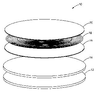
[0018] Referring to FIG. 1, a layered heater 10 constructed in
accordance with
the teachings of the present disclosure includes an application substrate 12,
a heater
substrate 14, a first dielectric layer 16 formed on the heater substrate 14, a
resistive
heating layer 18 formed on the first dielectric layer 16, and a second
dielectric layer 20
formed on the resistive heating layer 18. The first dielectric layer 16, the
resistive heating
layer 18 and the second dielectric layer 20 are formed by a layered process,
such as thick
film, thin film, thermal spray and sol gel.
[0019] Referring to FIG. 2, the layered heater 10 is joined to a heating
target 22
to form a heater assembly 25. For example, the heating target 22 may be a
chuck top of a
heated electrostatic chuck for semiconductor processing. The application
substrate 12
and the heater substrate 14 are made of different materials and are joined by
brazing to
form a composite chuck.
[0020] A brazing layer 24 is formed between the application substrate 12
and the
heater substrate 14. The brazing material may be a sliver brazing material.
Other joining
processes, such as welding, soldering, diffusion bonding, epoxying,
vulcanizing, may be
used to join the application substrate 12 and the heater substrate 14 without
departing
from the scope of the present disclosure. Similarly, the application substrate
12 may be
joined to the heating target 22 by any conventional joining method, such as
brazing,
welding, soldering, diffusion boding, epoxying, vulcanizing.
[0021] The application substrate 12 includes a material having a
coefficient of
thermal expansion (CTE) that matches the CTE of the heating target 22.
Alternatively, the
application substrate 12 may be an integral part of the heating target to
which the heat
from the layered heater is transferred. The heater substrate 14 includes a
material having
a CTE that matches the CTE of the first dielectric layer 16. In other words,
the material of
the application substrate 12 depends on the materials of the heating target
22, whereas
the material of the heater substrate 14 depends on the materials of the first
dielectric layer
16.
CA 02878338 2016-06-27
[0022] For example, when the first dielectric layer 16 includes alumina
ceramic, the heater substrate 14 may be made of alumina nitride or molybdenum.
The
application substrate 12 may include a material having a CTE that can easily
match the
CTE of most suitable materials for the heating target 22, regardless of the
materials of the
first dielectric layer 16 and the heater substrate 14. The application
substrate 12 may
include austenitic stainless steel, which has a CTE matching a wider selection
of
materials. Therefore, the layered heater 10 can be relatively easily joined to
the heating
target 22.
[0023] The layered heater 10 may be a layered heater formed by thick
film,
thin film, thermal-spray, and sol-gel process. The resistive heating layer 18
may be
formed by applying a resistive layer throughout the first dielectric layer 14,
followed by a
laser removal process to form a circuit pattern.
[0024] In still another form, the resistive heating layer 18 is formed
of a
material having sufficient temperature coefficient of resistance such that the
heating layer
18 functions as both a heater and a temperature sensor, commonly referred to
as "two-
wire control." Such heaters and their materials are disclosed, for example, in
U.S. Patent
No. 7,196,295 and U.S. patent application serial no. 11/475,534.
[0025] Referring to FIG. 3, a heater assembly 30 has a structure similar
to
that of the heater assembly 10 of FIG. 2 except that the layered heater
further includes a
bond coat layer 32 and a topcoat 34. The bond coat layer 32 is applied on the
heater
substrate 14. The topcoat 34 is applied on the second dielectric layer 20.
[0026] While two substrates are described in the present disclosure to
form a
composite substrate, more than two substrates may be used to form a composite
substrate, which provides a gradual transition over multiple substrates in
terms of
coefficient of thermal expansion.
[0027] Referring to FIG. 4, a method 40 of forming a heater assembly 25
for
use in semiconductor processing includes bonding an application substrate 12
to a
heating target 22 in step 42. When the application substrate 12 is an integral
part of the
heating target 22, this step is eliminated. The heater substrate 14 is then
thermally
secured to the application substrate 12 in step 44. Thermally securing may
include
brazing, welding, soldering, diffusion bonding, epoxying, vulcanizing at a
first
temperature. A layered heater is then applied to the heater substrate 14 after
the
application substrate 12 is joined to the heating target 22
4
CA 02878338 2015-01-02
WO 2014/008241 PCT/US2013/049038
[0028] The application of the layered heater on the heater substrate 14
includes
applying a first dielectric layer 16 on the heater substrate 14 in step 46. A
resistive heating
layer 18 is then applied on the first dielectric layer 16 in step 48. The
resistive heating
layer 18 may be applied to form a circuit pattern when applied on the first
dielectric layer
16. Alternatively, the resistive heating layer 18 may be applied by forming a
continuous
layer on the entire surface of the first dielectric layer 16, followed by a
laser removal
process to form the desired circuit pattern. Finally, a second dielectric
layer 20 is applied
on the resistive heating layer 18 in step 50. The method 40 ends in step 52.
[0029] Referring to FIG. 5, a method 60 of forming a heater assembly 30
for use
in semiconductor processing is similar to the method 40 of FIG. 4 except for
the steps of
applying a bond coat layer and a topcoat. More specifically, the method 60
includes
bonding the application substrate 12 to the heating target 22 in step 62. The
heater
substrate 14 is then thermally secured to the application substrate 12 in step
64.
Thermally securing may include brazing, welding, soldering, diffusion bonding,
epoxying,
vulcanizing at a first temperature. Thereafter, a layered heater is applied to
the heater
substrate 14 after the heater substrate 14 is joined to the application
substrate 12.
[0030] The application of the layered heater to the heater substrate 14
includes
applying a bond coat layer 32 on the heater substrate 14 in step 66. A first
dielectric layer
16 is then applied on the bond coat layer 32 in step 68. A resistive heating
layer 18 is
applied on the first dielectric layer 16 in step 70. A second dielectric layer
20 is applied on
the resistive heating layer 18 in step 72. A topcoat 34 is applied over the
second dielectric
layer 20 in step 74. Finally, portions of the topcoat 34 are removed to
achieve a
predetermined surface flatness in step 76. The method 60 ends in step 78.
[0031] In the methods 40 and 60 of the present disclosure, brazing is
used to
effectively and reliably join the heater substrate 14 to the application
substrate 12. The
application substrate 12 is made of a material having a CTE that matches the
CTE of the
material of the heating target 22. The heater substrate 14 is made of a
material having a
CTE that matches the CTE of the material of the first dielectric layer 16. The
composite
substrate enables the layer heater to be applied to a heating target 22 having
a CTE that
does not match (i.e., is significantly different from) the CTE of the heater
substrate 14.
[0032] Moreover, the brazing process, which requires a relatively high
temperature, is performed before the various functional layers of the layered
heater are
applied to the heater substrate 14. Therefore, the layered heater is not
subjected to the
undesirable high temperature during the brazing process and thus can maintain
its
integrity.
CA 02878338 2016-06-27
[0033] The present
method enables better matching of the CTE of the
layered heater to any heating target 22 by using an application substrate. The
present
method also ensures the integrity of the layered heater by brazing the heater
substrate to
the application substrate before the different functional layers of the
layered heater are
formed on the heater substrate. Therefore, the
present method can improve
physical/material characteristics of the heater assembly such as
machinability, surface
roughness, surface hardness, chemical compatibility, thermal conductivity,
electrical
conductivity, emissivity, appearance, cost, etc.
[0034] The scope of
the claims should not be limited by the preferred
embodiments set forth above, but should be given the broadest interpretation
consistent
with the description as a whole.
6