Note: Descriptions are shown in the official language in which they were submitted.
CA 02879618 2015-01-23
SYSTEM AND METHOD FOR REDUCTION OF SIGNAL DISTORTION
FIELD OF THE INVENTION
moil This invention relates to the suppression of distortion in electrical
signals. In
particular, this invention relates to a system and method for reducing
harmonic
distortion in complex signals containing multiple sine signals of various
frequencies or
for monochromatic signals with variable frequency.
BACKGROUND OF THE INVENTION
100021 Figure 1 illustrates a prior art signal-processing device 10, in the
example shown
a sound signal amplifier as a main distortion generator in the circuit. The
input 12
accepts a signal, for example a line level signal, from an audio source such
as a CD
player, musical DAC device or the like. The device 10 amplifies the input
signal and via
output 14 transmits the amplified signal to a transducer, for example
conventional
electromagnetically-driven speaker, to generate sound waves corresponding to
the
output electrical signal.
100031 The processing of any electrical signal, for example modulation-
demodulation,
analog-to-digital (ADC) and digital-to-analog (DAC) conversions or
amplification as in
the embodiment illustrated, can distort the signal waveform. According to
Fourier's
theorem, the damaged original sine signal (as with every periodical signal)
can be
represented as the sum of sine signals of divisible frequencies (harmonics),
the lowest
harmonic frequency (1st harmonic) being the fundamental frequency of the
original
signal. A coefficient of divisibility provides the number of each harmonic.
Under the
principle of superposition, all harmonics above the fundamental are additive
to the
original signal sine waveform and therefore cause signal distortion. Thus, in
order to
restore the original signal waveform, it is sufficient to suppress all
harmonics except the
1st harmonic (fundamental).
100041 If the original signal has a sine form of stable frequency, the
distorted signal can
typically be corrected by a high-quality resonance pass filter having the same
frequency
as the original elementary signal. Such a filter will pass only the original
signal
CA 02879618 2015-01-23
frequency, and thus eliminate higher harmonics to restore the original signal
waveform.
However, when the original signal contains two or more elementary (sine)
signals of
random frequencies, this method cannot be used to restore the original signal
waveform
from a processed signal.
100051 It would accordingly be beneficial to provide a system and method for
the
reduction of signal distortion in a processed signal consisting of multiple
frequency sine
cornponents.
BRIEF DESCRIPTION OF THE DRAWINGS
100061 In drawings which illustrate by way of example only a preferred
embodiment of
the invention,
100071 Figure 1 is a schematic diagram of a prior art signal-processing device
with
signal distortion generation.
100081 Figure 2 is a schematic diagram of the signal-processing device of
Figure 1 with
signal distortion suppression according to the invention.
100091 Figure 3 is a schematic diagram of a simplified example of an
embodiment of the
invention using based on operational amplifiers.
loom Figure 4 is a graph showing the frequency characteristics of the pre-
processor
and post-processor illustrated in Figure 3.
100111 Figure 5 is a graph showing the frequency characteristics of pre-
processor and
post-processor in an embodiment of the invention wherein the post-processor
does not
have active elements.
100121 Figure 6 is a schematic diagram of a simplified example of an
embodiment of the
invention using a passive post-processor.
100131 Figure 7 is a graph showing the frequency characteristics of the pre-
processor in
an embodiment of the invention wherein pre-processing is effected in a
plurality of steps
to minimize the distortion generated by active elements of the pre-processor.
CA 02879618 2015-01-23
100141 Figure 8 is a schematic diagram of a simplified example of an
embodiment of the
invention using a two-step pre-processor and a passive post-processor to
produce the
graph of Figure 7.
DETAILED DESCRIPTION OF THE INVENTION
100151 The invention provides frequency-dependent signal processing for an
electrical
signal containing multiple frequency sine components, whereby harmonics
generated
by the elementary sine signals of various frequencies can be suppressed
relative to
their respective elementary signals. The invention will be described in the
context of an
audio signal distorted as a result of processing through an audio amplifier
10, however
the principles of the invention apply to any electrical signal distorted as a
result of some
type of processing, including without limitation modulation-demodulation,
conversion
between analog and digital, amplification, pre-amplification, equalization
etc.
100161 The post-processor 40 is designed such that within a given frequency
range (or
ranges) the amplitude of a signal passing through the post-processor 40 is
reduced as
the frequency increases (i.e. for any two signals within the given frequency
range or
within each range of two or more given ranges, the signal with higher
frequency has a
lower transfer coefficient than the signal with the lower frequency), referred
to herein as
a "negative frequency gradient." Thus, because harmonics have higher
frequencies
than their respective elementary signals, in the post-processing stage
harmonics
generated within the main processing device will be suppressed more (or
amplified less)
than the corresponding fundamental signals from which the harmonics were
generated.
100171 However, this differential frequency suppression has a negative effect:
higher
frequency components of the original signal will have a lower transfer
coefficient than
lower frequency components, creating "frequency distortion."
100181 To compensate for frequency distortion created by the post-processor
40, a pre-
processor 20 is provided upstream of the input of the main processing device
(amplifier
10), as shown in Figure 2. The pre-processor 20 provides frequency-dependent
signal
processing having a generally opposite effect to that of the post-processor
40, i.e. within
a given frequency range (ranges) the amplitude of signal passing through the
pre-
.
CA 02879618 2015-01-23
processor 20 increases as the frequency increases (i.e. for any two signals
within the
given range or within each range of two or more given ranges, the signal with
lower
frequency has a lower transfer coefficient than the signal with the higher
frequency),
referred to herein as a "positive frequency gradient." In effect, the pre-
processor 20
boosts the higher frequency components of the input signal before they are
processed
by the main processing device, e.g. audio amplifier 10, and before the higher-
frequency
harmonics are generated. Accordingly, in the post-processing stage 40, as
harmonics
generated by the amplifier 10 are suppressed the higher frequency elementary
signals
that were boosted in the pre-processing stage are reduced generally to their
original
levels (proportionate to other elementary frequencies), reducing or
substantially
eliminating frequency distortion caused by the amplifier 10.
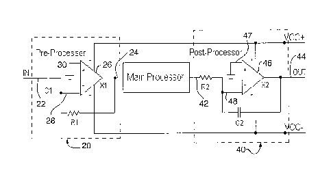
100191 Figure 3 illustrates a basic "ideal" embodiment of the invention, in
which the pre-
processor 20 comprises a differentiator and the post-processor 40 comprises an
integrator. In this embodiment both processors 20, 40 are based on operational
amplifiers. The pre-processor 20 illustrated has an input 22 connected to the
output of a
signal source (not shown), for example in the case of the audio amplifier 10
illustrated a
line-level output from a CD player, digital audio device or other sine signal
source.
100201 The source signal is passed to the inverting input 28 of op amp 26
through
capacitor C1 having a capacitance Cl F. The non-inverting input 30 of op amp
26 is
grounded. A feedback resistor R1 having a resistance R10 bridges the non-
inverting
input 28 and the op amp output 24.
100211 The pre-processed signal, inverted and intentionally frequency pre-
distorted by
the pre-processor 20, is fed to the input 12 of the main processing device, in
the
embodiment shown an audio amplifier 10, which produces a processed signal at
its
output 14. The processed signal, in addition to being pre-distorted by the
differentially
amplified frequencies produced by the pre-processor 20, is also distorted by
harmonics
generated during signal processing by the main processing device 10. The
processed
signal is passed to the input 42 of the integrator 40, through resistor R2
having a
resistance R20 to the inverting input 48 of op amp 46. The non-inverting input
47 of op
CA 02879618 2015-01-23
amp 46 is grounded. A feedback capacitor 02 having a capacitance C2F bridges
the
non-inverting input 48 and the op amp output 44.
100221 Figure 4 illustrates the frequency characteristics for pre-processor 20
and post-
processor 40 of Figure 3. The transfer coefficient K1 of pre-processor 20
depends on
signal frequency F' according to the formula:
K1 = 2 * Tr * F' * R1 Q * C1 F
This provides a positive frequency gradient +6 dB/octave. K1 = 1 for signal
frequency
F_dif, where:
F_dif = 1 / (2 * Tr * R1 0 * CIF)
100231 The transfer coefficient K2 of post-processor 40 depends on signal
frequency F"
according to the formula:
K2= 1 / (2 * Tr * F" * R20 * C2F)
This provides a negative frequency gradient -6 dB/octave. K2 = 1 for signal
frequency
F_int, where:
F_int = 1 1(2 * Tr * R20 * C2F)
100241 To achieve opposite signal processing for the pre-processor 20
(differentiator)
and post-processor 40 (integrator) and a substantially zero-effect on the
original signal
with simultaneous depression of harmonic distortion, the following ratio is
required:
F dif = F_int = F (the cross-point of the two plots on Figure 4). The
condition of this ratio
is: R1Q * C1F = R2Q * 02F. This produces the plots F' and F" for the pre-
processor 20
and post-processor 40, respectively, in Figure 4.
100251 Essentially, by amplifying high frequency components of the input
signal more
than the low frequency components of the input signal, the pre-processor 20
neutralizes
the frequency distortion that will be created by the post-processor 40 in the
course of
suppressing harmonics in the post-processing stage. Characteristics of the pre-
CA 02879618 2015-01-23
processor 20 and post-processor 40 should therefore be generally opposite in
order to
achieve a zero-sum effect at the output of the post-processor 40, as
illustrated in Figure
4 (wherein the signal level and frequency are illustrated in exponential
scales).
100261 Figure 5 illustrates frequency plots for the pre-processor 20 and post-
processor
40 in the situation where the post-processor 40 is composed only of passive
elements
such as resistors, capacitors and inductors. Such a passive device does not
generate
its own harmonic distortion, which can be necessary in some special
situations. The
processing range is between the frequencies Fl and F2. The post-processor 40
does
not amplify signals, but merely depresses them beginning from the frequency
Fl.
Between frequency plots Fl and F2 post-processor 40 has a negative frequency
gradient. Out of this range, its characteristic is linear. To compensate for
the frequency
distortion generated by the post-processor 40, the pre-processor 20 has a
positive
frequency gradient within the same range (between Fl and F2 plots). It
additionally
amplifies input signals, the highest amplification being at and above F2
frequencies.
100271 Figure 6 illustrates a simplified sample electrical scheme for the
device of the
invention utilizing a passive post-processor 50 comprising an inductor L1
having an
inductance L1H and resistor R4 having a resistance R40 connected in parallel,
which
transmits the signal from the output of the main processor 10 to a speaker 52
having an
impedance Z1 Feedback resistor R3 having a resistance R3c1 is coupled directly
between the output 24 of the pre-processor op amp 26 and inverting input 28.
Based on
an impedance Z1, frequencies Fl and F2 and, for example, a capacitance of C1,
in
order to achieve a zero-sum effect the values for the other electronic
components can
be calculated according to following formulas:
L1 H = Z1 / (2 * -rr * F1);
R4C1 = 2 * -rr * F2 * L1 H;
R20 = R30 = 1 / (2 * -rr * Fl * CIF)
R1 = 1 / (2 * * F2 * C1 F).
CA 02879618 2015-01-23
100281 This scheme has additional bonus. The impedance of inductor L1 depends
on
the frequency F of the signal. It is equal to Z1 (the impedance of the speaker
52) on Fl
and increases proportionally to frequency to F2 when it is limited by resistor
R4. For
frequencies above Fl, the "voltage output" amplifier 10 (Main Processor)
operates with
speaker 52 as a "current output" device. Speakers generally have an impedance
that
depends on frequency because of their interior inductance (for electro-
magnetic
devices) and capacitance (for piezoelectric devices), resonance features, etc.
The
output audio signal of speaker 52 depends on the current through its coil or
crystal, and
unstable impedance leads to instability of the audio signal in the case of a
"voltage
output" amplifier. Thus, the high output impedance of a "current output"
amplifier
stabilizes the speaker current and improves the linearity of its output.
100291 This scheme leaves the "voltage output" amplifier with its original low
output
impedance for frequencies under Fl. It may thus be necessary when operating
the
device of the invention with bass acoustic systems that have strong low
frequency
resonances to dampen the acoustic system by the low-impedance output of
"voltage
output" audio amplifier through the post-processor 50.
100301 Figure 7 illustrates transfer coefficient as a function of frequency in
the situation
where the frequency range F1--F2 of the signal being pre-processed is too wide
and
the amplification required by the pre-processor is high enough to generate
noticeable
distortion inside the pre-processor itself. In this case, pre-processing can
be done in two
(or more) steps with lower amplification in each step. The embodiment of
Figure 6
essentially divides the frequency range F1¨>F2 into two frequency ranges F1¨F3
and
F3¨>F2, and pre-processing is effected by two sub-processors within the pre-
processor
20, connected in-line (i.e. operating one after another). The first sub-
processor
produces plot Al --4k2¨>A3 and the second sub-processor has characteristic
B1¨>B2-433 superposed onto the upper limit of the first sub-processor. The
resulting
amplitude vs. frequency characteristic is A1¨>A2¨>B2.1¨>B3.1.
100311 Figure 8 illustrates an embodiment of the invention using an active pre-
processor
and a passive post-processor 50 as in Figure 6, however in the embodiment of
Figure 8
CA 02879618 2015-01-23
the pre-processor 60 comprises two sub-processors 20a, 20b, which combine to
produce the plots shown in the graph of Figure 7. Sub-processor 20a processes
the
input signal within the frequency range F1--F3 and sub-processor 20b processes
the
output of sub-processor 20a within the frequency range F3¨>F2 of Figure 7. The
operation of the embodiment of Figure 8 is otherwise similar to that of the
embodiment
of Figure 6.
100321 It will be appreciated that some harmonics have so little effect on the
amplified
source signal, particularly the highest harmonic frequencies, that it will not
always be
necessary to target all harmonics for suppression. It will also be appreciated
that some
frequencies may not require processing, depending upon the application; for
example in
the case of an audio signal it may be unnecessary to process frequencies above
the
upper or below the lower limits of human hearing, respectively, even though
the source
signal may comprises elementary frequencies having values beyond these
thresholds.
100331 It will also be appreciated that the system and method of the invention
can be
used for the depression of signal distortion generated as a result of non-
electronic
processes within a complex system such as radio transmitting/receiving,
transmission of
information signals through optical waveguides, acoustic delay elements etc.
100341 Embodiments of the present invention having been described in detail by
way of
example, it will be apparent to those skilled in the art that variations and
modifications
may be made without departing from the invention. For example, without
limitation, it will
be appreciated that the principles of the invention can be applied to any sine
signal as a
source signal, audio signals being heretofore described by way of non-limiting
example
only. The invention includes all such variations and modifications as fall
within the scope
of the claims.