Note: Descriptions are shown in the official language in which they were submitted.
AGILE IMAGING SYSTEM
FIELD OF THE INVENTION
[001] The present invention relates to the field of Optical Coherence
Tomography (OCT) imaging.
BACKGROUND
[002] Optical Coherence Tomography (OCT) is a non-invasive, interferometric
optical imaging technique that can generate micron resolution 2D and 3D images
of tissue
and other scattering or reflective materials. OCT is often used for biomedical
imaging or
materials inspection. First demonstrated for imaging the human eye and
coronary arteries
in 1991, OCT has since been established as a clinical standard for diagnosing
and
monitoring treatment of eye disease. OCT is also used for intravascular
imaging of
plaque to assess heart disease, cancer biopsy imaging, developmental biology
research, art
preservation, industrial inspection, metrology, and quality assurance.
[003] In general, OCT is useful for applications that benefit from
subsurface
imaging, surface profiling, motion characterization, fluid flow
characterization, index of
refraction measurement, birefringence characterization, scattering
characterization, or
distance measurement.
[004] Optical Coherence Tomography uses the interference pattern obtained
by
combining light backscattered or backreflected from a sample with light from a
reference
arm to determine spatially dependent properties of the sample, as illustrated
in Fig. 1A.
Time Domain OCT (TD-OCT) imaging principles were used in the first
demonstrations
and commercial products for OCT. However, TD-OCT is known to be a slow
technology
for acquiring OCT data. Fourier Domain OCT (FD-OCT) enables orders of
magnitude
- 1 -
CA 2880038 2019-08-15
CA 02880038 2015-01-23
WO 2014/018950
PCT/US2013/052425
faster imaging speeds than TD-OCT and has become the current research and
commercial
standard. Fourier Domain OCT can be implemented with a broadband light source,
interferometer, spectrometer, and linescan camera, called Spectral Domain OCT
(SD-
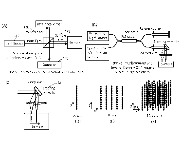
OCT), as illustrated in Fig. 1B. Scanning the light across a sample (Fig. 1C)
allows the
collection of a complete reflectivity vs. depth profile, called an A-scan
(Fig. 1D), for each
point of interrogation. Scanning and assembling sequentially acquired A-scans
allows
2D images to be formed, called B-scans (Fig. 1E). 3D volumes are also formed
by
scanning across the sample in two directions (Fig. 1F). Fourier Domain OCT can
also be
implemented with a wavelength swept light source, interferometer, detector,
and analog
to digital converter (AID), called Swept Source OCT (SS-OCT) or optical
frequency
domain imaging (OFDI), as illustrated in Figs. 2A and 2B. For the purposes of
this
disclosure, Swept Source OCT and OFDI are equivalent. The two variations of
Fourier
Domain OCT, being Spectral Domain OCT and Swept Source OCT, represent the
state of
the art in OCT imaging technologies.
[005] Spectral Domain OCT suffers from an inherent and problematic loss of
OCT sensitivity with increasing imaging depth, often called sensitivity roll-
off,
sensitivity fall-off, or sensitivity drop. The loss of OCT sensitivity with
increasing depth
is caused by a reduction in the interferometric fringe visibility due to
limits in the
spectrometer resolution, integration of multiple wavelengths over a pixel
width, and
inter-pixel crosstalk, as described in the papers, "Analytical model of
spectrometer-based
two-beam spectral interferometry," Hu, Pan, and Rollins, Applied Optics, Vol.
46, No.
35, pp. 8499-8505, 2007 and "Improved spectral optical coherence tomography
using
optical frequency comb," Bajraszewski et al. Optics Express, Vol. 16, No. 6,
pp. 4163-
4176, 2008.
[006] A paper, "Fourier domain optical coherence tomography with a linear-
in-
wavenumber spectrometer, "Hu and Rollins, Optics Letters, Vol. 32, No. 24, pp.
3525-
3527, 2007, teaches linearizing the spectral dispersion of the spectrometer in
wavenumber using a specifically designed prism. The spectral linearity in
wavenumber
- 2 -
CA 02880038 2015-01-23
WO 2014/018950
PCT/US2013/052425
results in improvement of the fall-off of signal with imaging range inherent
to spectral
domain optical coherence tomography imaging. Although there is improvement,
the loss
of sensitivity with imaging depth is still significant, especially when used
with wide
spectral bandwidth sources for achieving a fine OCT axial resolution.
[007] A paper, "Improved spectral optical coherence tomography using
optical
frequency comb," Bajraszewski et al. Optics Express, Vol. 16, No. 6, pp. 4163-
4176,
2008, teaches using a Fabry-Perot optical frequency comb in a Spectral Domain
OCT
system to reduce the depth dependent drop of sensitivity. The approach has
several
significant disadvantages. Insertion of the frequency comb reduces optical
power levels,
which compromises baseline OCT sensitivity. The approach also requires that
the optical
frequency comb be actively tuned and multiple spectrometer measurements
performed
for every A-scan in order to fill gaps in spectral data content that are
filtered out by the
Fabry-Perot filter. In practice, four camera exposures were shown to enable
OCT
imaging, which results in a significant reduction in OCT imaging speed.
[008] Various so called "full range" or "complex conjugate" approaches have
been proposed to extend the imaging range and help mitigate the problem of
sensitivity
roll-off associated with Spectral Domain OCT. These approaches do not fully
suppress
complex conjugate artifacts in the images, require considerable computation,
and often
require multiple acquisitions to construct each A-scan, so are not suitable
for high
dynamic range and high speed OCT acquisition. Further, maximum imaging speeds
with
Spectral Domain OCT are limited to several hundred kilohertz A-scan rate due
to limits
in linescan camera speeds. These inherent characteristics and deficiencies
combined
suggest that Spectral Domain OCT is not the technology of choice for long
range, high
speed, and high dynamic range imaging.
[009] Swept Source OCT uses a wavelength swept laser as the light source
and a
detector with high speed AID converter to sample the interferometric OCT
signal.
Sensitivity roll-off performance in Swept Source OCT is generally
significantly better
- 3 -
CA 02880038 2015-01-23
WO 2014/018950
PCT/US2013/052425
than Spectral Domain OCT. Swept Source OCT has also achieved higher imaging
speeds
and longer imaging range than Spectral Domain OCT.
[010] Many different swept laser configurations and wavelength tuning
mechanisms have been implemented for Swept Source OCT that either include a
wavelength selective intracavity filter or wavelength selective laser cavity
end minor.
Examples include: galvo-grating wavelength selective end mirror designs
(Chinn,
Swanson, and Fujimoto, Optics Letters, Vol. 22, No. 5, pp. 340-342, 1997),
rotating
polygon minor-grating filter designs (Yun et al., Optics Letters, Vol. 28, No.
20, pp.
1981-1983, 2003), fiber ring lasers with intracavity wavelength selective
filter (Huber et
al., Optics Express Vol. 13, No. 9, pp. 3513-3528, 2005), and short cavity
microelectromechanical systems (MEMS) filter based tunable lasers (WO
2010/111795
Al ). In all of these swept laser designs, lasing builds from amplified
spontaneous
emission (ASE) as the filter is tuned such that the photon round trip time is
significant,
and along with cavity efficiency and filter width, define a maximum sweep
speed at
which the laser can be swept while still maintaining full saturation of the
optical gain
medium. Sweep repetition rates in the tens of kilohertz to low hundreds of
kilohertz are
generally possible with these technologies, but the sweep speed is still
fundamentally
limited due to the relatively long photon round trip time.
[011] U.S. Patent Application No. 2006/0187537 Al teaches a different swept
source laser technology, called a Fourier Domain Mode Locked (FDML) laser. An
FDML laser operates with a principle that enables higher sweep speeds. In an
FDML
laser, a long fiber loop is used to store the wavelength sweep and a filter is
tuned in
synchronization with the returning sweep wavelength, either before or after
optical
amplification. The FDML approach reduces the need to build up lasing from ASE
to
achieve high fundamental sweep repetition rates up to about 500 kHz axial scan
rate.
Through replicating, delaying, and multiplexing the sweep, buffered speeds up
to about 5
MHz axial scan rate can be achieved for a single imaging spot (Wieser et al.,
Optics
Express, Vol. 18, No. 14, 2010). A significant drawback of a typical FDML
laser is a
- 4 -
CA 02880038 2015-01-23
WO 2014/018950
PCT/US2013/052425
short a coherence length of about 4-10 mm, which significantly limits OCT
imaging
range.
[012] In Swept Source OCT, sensitivity roll-off is limited by the coherence
length of the wavelength tunable laser source, which is determined by the
instantaneous
linewidth of the laser. In all of the swept lasers describe thus far, the
filter in the laser is
designed to tune multiple laser longitudinal modes. As taught by International
Patent
Application Publication No. WO 2010/111795 Al and Huber et al., Optics Express
Vol.
13, No. 9, pp. 3513-3528, 2005, the wavelength selective filter in a
traditional swept laser
design spans multiple longitudinal laser modes in order to achieve high sweep
rates and
prevent laser power drop off and laser noise due to mode-hopping. In the case
of the
FDML laser, the reason for designing a relatively wide spectral filter width
is related to
dispersion in the fiber loop that causes a wavelength dependent round trip
time, requiring
the filter to be wide enough to transmit the full range of slow to fast
wavelengths in the
fiber loop. Regardless of the reason for needing to use a wide filter that
spans multiple
laser longitudinal modes, the result is a laser with a relatively wide
instantaneous
linewidth with compromised coherence length, OCT imaging range, and OCT
sensitivity
roll-off.
[013] A paper, "Extended coherence length Fourier domain mode locked lasers
at 1310 nm", Adler et al., Optics Express, Vol. 19, No. 21, pp. 20931-20939,
2011
teaches a method to improve the coherence length of an FDML laser by adding a
chirped
fiber Bragg grating dispersion compensation module to improve the dispersion
characteristics of the fiber loop. Improved laser coherence length to about
21mm and the
ability to use both the forwards and backwards sweeps were obtained.
[014] In nearly all implementations to date, Spectral Domain OCT systems
and
Swept Source OCT systems have been designed to operate at a fixed imaging
speed,
fixed imaging range, and fixed OCT axial resolution. Generally, the entire OCT
imaging
system is optimized for a specific application.
- 5 -
CA 02880038 2015-01-23
WO 2014/018950
PCT/US2013/052425
[015] With the introduction of high speed CMOS lincscan camera technology
with programmable speed and programmable active pixel count, it became
possible to
trade off pixel count to gain imaging speed in Spectral Domain OCT.
[016] A paper, "Ultrahigh speed Spectral / Fourier domain OCT ophthalmic
imaging at 70,000 to 312,500 axial scans per second," Potsaid et al., Optics
Express, Vol.
16, No. 19, pp. 15149-15169, 2008, teaches operating a Spectral Domain OCT
system
using a CMOS camera with adjustable active pixel count in different
configurations to
achieve: long imaging range with fine axial resolution and moderate OCT
imaging speed,
short imaging range with fine axial resolution at faster imaging speeds, and
short imaging
range with compromised axial resolution at ultrafast imaging speeds. Each
configuration
was optimized for sensitivity and imaging performance. A significant drawback
of the
approach is that the light source must be interchanged and the spectrometer
rebuilt with
different components for the multiple configurations and operating modes.
[017] A paper, "High-Speed High-Resolution Optical Coherence Tomography at
800 and 1060 nm", Povazay et al., Proceedings of SPIE, vol. 7139, pp. 71390R-1-
7,
2008, teaches an OCT imaging system using a programmable CMOS camera with a
fixed
light source in which the number of pixels used in the camera is reduced in
order to
achieve higher imaging speeds by truncating the spectrum. A significant
disadvantage of
this method is that the spectrometer is not reoptimized to the light source
bandwidth for
the different operating modes, so light falls on unused pixels for the higher
speed imaging
configurations and there is an associated loss of OCT sensitivity.
[018] A paper, "Ultra high-speed swept source OCT imaging of the anterior
segment of human eye at 200 kHz with adjustable imaging range," Gora et al,
Optics
Express, Vol. 17, No. 17, pp. 14880-14894, 2009, teaches a Swept Source OCT
imaging
systems using an FDML laser that trades off OCT axial resolution to gain
imaging range.
A disadvantage of this approach is that the FDML laser must be run at a
harmonic of the
sweep frequency, so the sweep repetition rate of the OCT imaging system cannot
be
changed without significant reconfiguration.
- 6 -
CA 02880038 2015-01-23
WO 2014/018950
PCT/US2013/052425
[019] A new swept light source for use with Swept Source OCT has been
developed that overcomes many of the above mentioned limitations associated
with
previous OCT technologies.
[020] U.S. Patent No. 7468997 B2 teaches a swept source optical coherence
tomography system (SS-OCT) comprising a vertical cavity surface-emitting laser
(VCSEL) with an integrated MEMs tunable mirror movable by electro-static
deflection.
A paper, "OCT Imaging up to 760 kHz Axial Scan Rate Using Single-Mode 1310 nm
MEMS-Tunable VCSELs with >100nm Tuning Range," Jayaraman et al., Optical
Society of America, CLEO Conference, pp. PDPB1-PDPB2, 2011, experimentally
demonstrates the first widely tunable, single-mode 1310 nm MEMS VCSELs with
>100
nm tuning range, and the first application of these VCSELs to ultra-high-speed
swept
source OCT imaging at axial scan rates up to 760 kHz. Unlike other swept laser
sources,
which use a short cavity and intra-cavity filter, VCSELs operate with a true
single-
longitudinal mode instead of a set of modes. The true single-longitudinal mode
operation
results in a long coherence length for the VCSEL technology. Further, forward
and
backward scans show comparable performance, in contrast to other swept
sources,
enabling use of both the forwards and backwards sweeps for OCT imaging.
[021] The limited imaging speed, limited imaging range, loss of sensitivity
with
increasing imaging depth, and operation at a predominately fixed imaging mode
of
previous OCT technologies result in a compromise of OCT imaging performance
and
limit application of OCT technology.
SUMMARY
[022] An embodiment of the present invention is an optical coherence
tomography imaging system using a vertical cavity laser (VCL) source and
methods for
its operation. Unique and advantageous capabilities and functionalities of
embodiments
of the present invention are enabled by the incorporation of a new tunable VCL
source
technology in a novel imaging system architecture. An embodiment of the
present
invention offers speed, imaging range, and size improvements over existing
approaches.
- 7 -
CA 02880038 2015-01-23
WO 2014/018950
PCT/US2013/052425
Further, an embodiment of the present invention enables switching between
different
imaging modes defined by imaging speed, imaging range, and imaging resolution,
making the present invention more agile and flexible during use when compared
to
existing approaches. One embodiment offers enhanced dynamic range imaging
capability for accommodating bright reflections. One embodiment offers
multiscale
imaging capability for measurement over orders of magnitude dimensional
scales. The
imaging system and methods for generating the waveforms to drive the tunable
laser in
flexible and agile modes of operation are also described. The possible areas
of use
include medical imaging, biological imaging, industrial inspection, material
inspection,
subsurface imaging, surface profiling, distance ranging and measurement, fluid
flow
characterization and analysis, and investigation and characterization of
material
polarization properties.
[023] One
embodiment provides an optical imaging system, including: a tunable
source including a wavelength tunable vertical cavity laser (VCL) and
intracavity tuning
element generating a single longitudinal mode output that is tunable over an
emission
wavelength range for generating wavelength sweeps; a tuning driver, the tuning
driver
being capable of generating one or more wavelength tuning waveforms to affect
the
tuning element which determines the sweep trajectory, sweep speed, sweep
repetition
rate, sweep linearity, and emission wavelength range; a current driver that
supplies
current to a gain material within the tunable source to adjust output optical
radiation
power; a monitoring detector to measure attributes of the tuning response and
provide
feedback to correct for disturbances to the tunable source or to generate
wavelength
tuning waveforms; an optical interferometer with a reference arm and a sample
arm
illuminated by said tunable source; one or more optical detectors that convert
optical
interference fringe signals from the optical interferometer into electric
analog signals; a
data acquisition device to convert the electric analog signals output from the
one or more
detectors into digital data.
- 8 -
CA 02880038 2015-01-23
WO 2014/018950
PCT/US2013/052425
[024] Another embodiment provides an optical coherence tomography imaging
system including: a VCL source that has the characteristics of being able to
image over
adjustable depth ranges, axial resolutions, and at continuously adjustable
speeds, the
optical coherence tomography system being able to image over an extended
imaging
range enabled by the long coherence length of the VCL source.
[025] Another embodiment provides a method for generating a tuning waveform
of the above optical imaging system, the method including: expressing the
tuning
waveform as a function of adjustable input parameter values to create a tuning
waveform
expression; applying the tuning waveform to the tuning element or a
mathematical model
of the tunable source dynamics to generate at least one experimental
measurement or
simulated wavelength sweep; calculating a value of a performance metric or an
objective
function based on the experimental measurement or the simulated wavelength
sweep;
adjusting the value of the input parameters to optimize the value of the
performance
metric or objective function.
BRIEF DESCRIPTION OF THE DRAWINGS
[026] Figure 1 is a set of drawings illustrating OCT system layouts and OCT
scanning.
[027] Figure 2 is a set of drawings illustrating Swept Source OCT system
layouts.
[028] Figure 3 is a set of drawings and plots illustrating Swept Source OCT
fringe formation.
[029] Figure 4 is a set of plots illustrating sweep trajectory and fringe
envelope
effects on OCT acquisition and point spread function formation.
[030] Figure 5 is a block diagram of an imaging system.
[031] Figure 6 is set of drawings, photographs, and plots illustrating a
MEMS-
tunable Vertical Cavity Surface Emitting Laser (MEMS-VCSEL).
[032] Figure 7 is a set of plots illustrating wavelength sweep ranges of
MEMS-
tunable VCSELs.
- 9 -
CA 02880038 2015-01-23
WO 2014/018950
PCT/US2013/052425
[033] Figure 8 is a set of drawings and plots illustrating multimode and
single
mode tuning principles and coherence length of OCT imaging technologies.
[034] Figure 9 is a set of plots and photographs illustrating the effect of
MEMS
actuator geometry on the dynamic response of the MEMS actuator.
[035] Figure 10 is a collection of oscilloscope screen images showing a
single
tunable source being driven at different sweep repetition rates from 100 kHz
to 400 kHz.
[036] Figure 11 a plot showing the spectral response of a single tunable
source
being driven at different sweep repetition rates from 100 kHz to 400 kHz.
[037] Figure 12 is a plot showing variable wavelength range tuning of a
single
tunable source.
[038] Figure 13 is a set of block diagrams illustrating embodiments of the
tunable source of the present invention.
[039] Figure 14 is a set of block diagrams illustrating embodiments of the
tunable source of the present invention comprising optical amplifiers.
[040] Figure 15 is a set of block diagrams of a wavelength tuning
subsystems.
[041] Figure 16 is a set of oscilloscope screen images showing the tuning
response of a VCSEL driven at 100 kHz with a linearized sweep driven by a
custom
waveform.
[042] Figure 17 is a collection of plots showing linearized sweep
performance.
[043] Figure 18 is a plot showing the optical spectrum of a VCSEL driven at
100
kHz driven by a custom waveform.
[044] Figure 19 is an oscilloscope screen capture showing bidirectional and
linearized sweep trajectories.
[045] Figure 20 is a plot and image showing the tuning response of a
tunable
source and the associated image of a human finger obtained at 500 kHz sweep
repetition
rate.
[046] Figure 21 is a collection of images showing imaging at two different
imaging ranges.
- 10 -
CA 02880038 2015-01-23
WO 2014/018950
PCT/US2013/052425
[047] Figure 22 is a block diagram of closed loop method of waveform
generation.
[048] Figure 23 is a flow chart illustrating a method for tuning driver
waveform
synthesis.
[049] Figure 24 is a block diagram of a closed loop wavelength tuning
subsystem.
[050] Figure 25 is a block diagram of a closed loop wavelength tuning
subsystem with optical amplifier.
[051] Figure 26 is a block diagram of a closed loop wavelength tuning
subsystem with optical amplifier and current driver.
[052] Figure 27 is a set of drawings and plots illustrating a method of
sweep
measurement based on an interferometric fringe.
[053] Figure 28 is a set of drawings and plots illustrating a method of
sweep
measurement based on detection of split power levels.
[054] Figure 29 is a flow chart illustrating a method of current driver
waveform
synthesis.
[055] Figure 30 is a set of drawings illustrating wavelength sweep
measurement
with feedback for wavelength sweep and envelope control.
[056] Figure 31 is a block diagram of an OCT imaging system showing optical
and electrical interconnections.
[057] Figure 32 is a block diagram of an OCT imaging system showing details
of an imaging system that uses an optical path delayed reference arm, optical
clocking,
and an optical wavelength trigger.
[058] Figure 33 is a block diagram of an OCT imaging system showing details
of an imaging system that use circulators, an optical wavelength trigger, and
optical
clocking.
[059] Figure 34 is a block diagram of a tunable source with adjustable
optical
clocking module.
-11-
CA 02880038 2015-01-23
WO 2014/018950
PCT/US2013/052425
[060] Figure 35 is a set of drawings illustrating an adjustable path length
interferometer and dispersion compensation.
[061] Figure 36 is a set of drawings illustrating adjustable path length
interferometers with a retroreflector and with circulators.
[062] Figure 37 is a set of drawings illustrating methods for selecting an
optical
path in one arm of the interferometer.
[063] Figure 38 is a set of drawings illustrating methods for selecting an
optical
path in one arm of the interferometer or for using dispersion compensation in
the
interferometer.
[064] Figure 39 is a set of electronic schematics showing counting logic.
[065] Figure 40 is a drawing showing the combination of selecting the path
length in an interferometer arm combined with frequency division and frequency
multiplication.
[066] Figure 41 is a set of OCT cross sectional images illustrating
expanded
dynamic range imaging.
[067] Figure 42 is a set of block diagrams illustrating sweep data
initiation using
an input to the trigger of the acquisition system.
[068] Figure 43 is a set of block diagrams illustrating sweep phase
stabilization
using multiple channels of AID conversion to perform the synchronization.
[069] Figure 44 is a block diagram illustrating a tunable optical trigger
generator.
[070] Figure 45 is a block diagram and a plot showing sweep phase
stabilization
using a Fabry-Perot filter.
[071] Figure 46 is a block diagram and plot illustrating sweep phase
stabilization
using a Fabry-Perot filter with a fast and slow AID converter.
[072] Figure 47 is a collection of plots showing phase stabilization using
time
delay estimation applied to different OCT system operating modes.
- 12 -
CA 02880038 2015-01-23
WO 2014/018950
PCT/US2013/052425
[073] Figure 48 is a block diagram of an imaging system with data
processing,
data storage, and data display capability.
[074] Figure 49 is a block diagram of a data stream showing compression of
the
data and storage of the data on a RAID array.
[075] Figure 50 is a block diagram of a sweep repetition rate multiplier
using
multiple VCL sources.
[076] Figure 51 is a block diagram of a sweep repetition rate multiplier
using a
single VCL source.
[077] Figure 52 is a block diagram of a closed loop wavelength tuning
subsystem and optical amplifier with tunable filter to suppress sidemodes and
amplified
spontaneous emission.
[078] Figure 53 is a block diagram of a closed loop wavelength tuning
subsystem with multiple optical amplifiers and a tunable filter positioned
between the
amplifiers to suppress sidemodes and amplified spontaneous emission.
[079] Figure 54 is a block diagram of a closed loop wavelength tuning
subsystem with temperature controlled gain material and a noise cater to
reduce laser
noise.
DETAILED DESCRIPTION
[080] The description of illustrative embodiments according to principles
of the
present invention is intended to be read in connection with the accompanying
drawings,
which are to be considered part of the entire written description. In the
description of
embodiments of the invention disclosed herein, any reference to direction or
orientation
is merely intended for convenience of description and is not intended in any
way to limit
the scope of the present invention. Relative terms such as "lower," "upper,"
"horizontal,"
"vertical," "above," "below," "up," "down," "top" and "bottom" as well as
derivative
thereof (e.g., "horizontally," "downwardly," "upwardly," etc.) should be
construed to
refer to the orientation as then described or as shown in the drawing under
discussion.
These relative terms are for convenience of description only and do not
require that the
- 13 -
CA 02880038 2015-01-23
WO 2014/018950
PCT/US2013/052425
apparatus be constructed or operated in a particular orientation unless
explicitly indicated
as such. Terms such as "attached," "affixed," "connected," "coupled,"
"interconnected,"
and similar refer to a relationship wherein structures are secured or attached
to one
another either directly or indirectly through intervening structures, as well
as both
movable or rigid attachments or relationships, unless expressly described
otherwise.
Moreover, the features and benefits of the invention are illustrated by
reference to the
exemplified embodiments. Accordingly, the invention expressly should not be
limited to
such exemplary embodiments illustrating some possible non-limiting combination
of
features that may exist alone or in other combinations of features; the scope
of the
invention being defined by the claims appended hereto.
[081] This disclosure describes the best mode or modes of practicing the
invention as presently contemplated. This description is not intended to be
understood in
a limiting sense, but provides an example of the invention presented solely
for illustrative
purposes by reference to the accompanying drawings to advise one of ordinary
skill in the
art of the advantages and construction of the invention. In the various views
of the
drawings, like reference characters designate like or similar parts.
[082] This detailed description describes embodiments of the present
invention
and is broken into sections related to the different aspects of the present
invention for
clarity.
[083] OCT Imaging Applications of the Preferred Embodiment
[084] The preferred embodiment of the present invention offers traditional
OCT
imaging performance superior to previously demonstrated OCT technologies when
used
in many existing OCT applications, such as the applications described in the
Background
section of this disclosure and including ophthalmic imaging, intravascular
imaging,
cancer biopsy imaging, developmental biology research, medical diagnostics,
surgery
guidance, art preservation, industrial inspection, metrology, and quality
assurance. More
generally the present invention can be practiced for applications that benefit
from
subsurface imaging, surface profiling, motion characterization, fluid flow
- 14 -
CA 02880038 2015-01-23
WO 2014/018950
PCT/US2013/052425
characterization, index of refraction measurement, birefringence
characterization,
scattering characterization, or distance measurement. The preferred embodiment
can be
practiced in all fields in which OCT imaging would be considered.
[085] The preferred embodiment offers OCT imaging capability previously not
available, including: extremely long imaging range, high fundamental imaging
speeds,
and ability to change imaging speed, imaging sweep trajectory, imaging
resolution, and
imaging range on the fly to support multiple modes of OCT imaging. The
preferred
embodiment also offers new enhanced dynamic range imaging capability for
accommodating bright reflections and multiscale imaging capability for
measurement
over orders of magnitude dimensional scales. The new capabilities of the
preferred
embodiment make the present invention enabling for new applications of OCT.
For
example, the present invention enables imaging, profiling, and measurement of
large
objects and samples in a manufacturing, diagnostic, medical, or research
environment.
Examples of new applications include placing a sample delivery optic or
scanner on the
end of a robot arm or gantry for inspection of manufactured goods by surface
profiling
and distance measurement, measuring part placement during assembly, inspecting
parts
for wear or damage, investigating stress levels in materials, and other
applications. The
different imaging modes of the OCT system can be selected by a user as
required by the
imaging application at hand, can be preprogrammed to switch according to a
schedule or
plan, as would be useful in a manufacturing environment, or can be adapted by
an
algorithm based on OCT measurements performed in realtime.
[086] From an original equipment manufacturer (OEM) perspective, the
flexible
operation of the preferred embodiment of the present invention allows a single
core OCT
module or engine to be used in multiple products or in a single product for
multiple
applications, thereby simplifying system design, stocking, and inventory
control in
addition to offering higher value to the customer.
[087] OCT Detection Methods And Principles
- 15 -
CA 02880038 2015-01-23
WO 2014/018950
PCT/US2013/052425
[088] The preferred embodiment uses OCT detection methods which operate by
interferometrically detecting backscattered and reflected light from a sample.
All OCT
systems comprise at a minimum a light source 110, interferometer with sample
arm 120
and reference arm 130, and a detector 140 to acquire the interferometric
signal, as
illustrated in Fig. 1A.
[089] The preferred embodiment uses a scanner for scanning the sample light
across the sample. The scanner in one embodiment is a rotating mirror as is
common in
ophthalmic OCT, a side viewing rotating probed as is common in intravascular
OCT, a
forwards looking probe with lateral scanning capability, or any other method
for scanning
light across the sample. The scanner in one embodiment is a moving stage or
conveyor
belt, allowing the OCT optics to remain stationary and unactuated. The scanner
in
another embodiment is a mobile robot, robotic arm, gantry, or other actuated
motion
generating platform, with either an unactuated sample arm optic or a sample
arm optic
with integrated scanning capability. Using the example of a galvanometer and
mirror
based scanner 150 that is common in OCT and shown in Fig. IC, OCT data
acquisition is
described next. OCT systems generally focus a light spot on a sample and
collect a
reflectivity vs. depth profile at a single transverse location on the sample,
called an A-
scan (Fig. 1D). The light spot on the sample can be scanned across the sample
and
multiple depth interrogations performed, each depth interrogation being an A-
scan.
Assembling the sequential A-scans obtained as the beam is scanned across the
sample
generates a 2D image of the sample, called a B-scan (Fig. 1E) or sometimes
called an
OCT cross sectional image. Multiple B-scans can be acquired using a raster
scanning
pattern to collect a 3D volumetric data set (Fig. 1F). Other scan patterns are
possible,
such as circles, concentric circles, spirals, or parking the scanners in one
location to get
multiple A-scans from the same location, called M-mode imaging. M-mode imaging
is
useful for imaging dynamic processes and can achieve a high temporal sample
rate to
capture fast dynamics. However, M-mode imaging is limited to obtaining
information
localized to a line in the sample corresponding to the A-scan location because
there is no
- 16 -
CA 02880038 2015-01-23
WO 2014/018950
PCT/US2013/052425
scanning performed. Acquiring multiple 3D data sets from the same location on
the
sample can generate 4D OCT data to form a volumetric time dependent movie of
the
sample, but at a reduced frame rate compared to M-mode imaging. Lower order
time
dependent acquisitions can be acquired, such as repeating a B-scan at the same
location,
to create a 2D movie. Repeating B-scans is also used to detect small changes
in the
sample over time, indicative of action or motion within the sample. Repeating
B-scans as
part of the collection of a 3D volume can generate 3D volumes that
characterize motion
on a time scale faster than allowed by repeating the full 3D volume. The scan
patterns
described so far generally relate to point sampling or point scanning OCT
methods. It is
also possible to perform parallel detection by implementing line scan OCT or
full field
OCT, using a 1D array camera or 2D array, respectively, or imaging with
multiple spots,
which are also included in some embodiments of the current invention.
1090] The preferred embodiment of the present invention implements swept
source OCT. Many optical designs can be used to construct the OCT
interferometer with
the preferred design being application and cost specific. Two possible
interferometer
designs are shown in Figs. 2A and 2B. These figures show different sample arm
light
delivery optics, one design for compatibility with the optics in the human eye
(Fig. 2A)
and one for imaging a more standard sample without integrated optics (Fig.
2B). Sample
arm delivery optics and interferometer designs can be interchanged as
appropriate to the
imaging application. Interferometer designs and sample optics different than
those
shown are possible and included in an embodiment of the present invention. In
general,
the interferometer and sample arm optics will be optimized for a specific
application or
class of applications. Fiber optic components used in the interferometer can
simplify
alignment and improve stability, although bulk optics interferometers can also
be used.
One embodiment of the present invention uses an interferometer comprising bulk
optics.
Another embodiment of the present invention uses an interferometer comprising
fiber
optic components. OCT systems can be built with bulk optics interferometers or
fiber
interferometers or a combination of both. The interferometer design
illustrated in Fig. 2A
- 17 -
CA 02880038 2015-01-23
WO 2014/018950
PCT/US2013/052425
works for OCT imaging at all wavelengths, but a portion of the light collected
by the
sample is redirected to the source through the first fiber coupler 210 and
never reaches
the detector, resulting in a loss of interferometer efficiency. The design
illustrated in
Fig. 2B includes circulators 220, 230. High efficiency circulators are
available at 1310
nm and other wavelengths, whereas circulators at 850 nm and 1050 nm
wavelengths are
less efficient. One embodiment of the present invention uses circulators to
improve
interferometer efficiency.
[091] Swept Source OCT systems operate by sweeping an emission wavelength
in time, using the emission as an input to an OCT interferometer, detecting
the
interferometric signal from the interferometer, and digitizing the signal for
analysis, as
illustrated in Fig. 3A. For illustrative purposes, the example fringe 310
shown in Fig. 3A
is roughly the fringe pattern that would be expected from a single mirror
reflection as
recorded by a Swept Source OCT system. To understand Swept Source OCT imaging
principles and system limitations, it is helpful to consider the OCT signal
from a mirror
reflection under different imaging configurations. Refer to Eq. 1 below, where
km is the
wavenumber at sample point in , I[km] is the instantaneous photocurrent at
sample point
, p[lc] is the detector responsively at sample point in, S[km] is the
instantaneous
power on the sample at sample point in, R, is the reflectivity of the
reference mirror,
Rs is the reflectivity of the sample mirror, Zr is the depth of the reference
mirror, and zs
is the depth of the sample arm mirror. Equation 1 was adapted from J.A. Izatt
and M.A.
Choma, Section 2.7, W. Drexler and J.G. Fujimoto Ed., "Optical Coherence
Tomography: Technology and Applications", 2008. In practice, the photocurrent,
I, is
generally transformed into a voltage by a transimpedance amplifier before AID
digitization.
I[km]=P[kmi S[km](R, + Rs +211R,R, cos(2k. (z, ¨z,)) [092] Eq. 1
2
- 18 -
CA 02880038 2015-01-23
WO 2014/018950
PCT/US2013/052425
[093] The term inside the cosine function represents the phase of the OCT
fringe. As the phase increases (or decreases), the OCT fringe oscillates with
a full period
of oscillation occurring every 2*m radians. A wavelength sweep has a starting
wavenumber, k,tõrt , and an ending wavenumber, ken,/. The number of
oscillations in
the OCT fringe is proportional to the magnitude of the total phase difference,
AO , over
the sweep, which is given by
[094] = 2(kõd ¨ k
start)(1r rs) = Eq. 2
[095] Equation 2 shows that the fringe frequency increases with increasing
imaging depth (i.e., there is a larger number of oscillations over the sweep)
because the
(Zr ¨zs) multiplier term inside the cosine function increases total fringe
phase, as
illustrated in Fig. 3B. All other sweep characteristics being equal, the
fringe frequency
increases with increasing sweep repetition rate for a given mirror position,
as illustrated
in Fig. 3C, because the same number of fringe oscillations occur over a
shorter time.
Similarly, with all other sweep characteristics being equal, the fringe
frequency increases
with increasing wavelength sweep range for a given mirror position, as
illustrated in Fig.
3D, because the total phase difference increases due to the larger (kõd ¨
kstart) term.
Fig. 4A shows an additional effect on fringe frequency in that the fringe
frequency is also
determined by the sweep trajectory. A sweep that has slow and fast portions,
such as that
produced with a sine wave trajectory 410 for example, has a peak fringe
frequency where
rate of change in wavenumber (k) vs. time is greatest. To the designer of an
OCT
imaging system, the consequences of these effects on fringe frequency are
significant
because of limitations and challenges associated with detecting and digitizing
the fringe.
In order to prevent aliasing of the fringe signal, the analog to digital
converter (AID) 320
must sample at least two times as fast as the fringe frequency, according to
Nyquist
sampling criteria. It is therefore preferential to linearize the sweep
frequency so that the
sweep is linear 420 in k-space (wavenumber) vs. time, as shown in Fig. 4A
bottom, or to
more generally minimize the peak fringe frequency to maximize OCT imaging
range for
- 19 -
CA 02880038 2015-01-23
WO 2014/018950
PCT/US2013/052425
a given maximum digitization rate. As the sampling rate of A/D converters
increases,
the cost of the A/D itself increases along with the cost, complexity, and
timing
requirements of the associated support electronics, data streaming mechanisms,
and data
storage. It is therefore often not feasible to simply choose a fast A/D
converter rate and a
compromise must be made in maximum obtainable data bandwidth (analog detection
bandwidth, AID rate, data streaming, and storage) according to what the market
will
support for the intended imaging application.
[096] For a given maximum acquisition bandwidth and AID conversion rate,
tradeoffs must be made in the OCT system design between instrument imaging
range,
sweep repetition rate (with associated OCT instrument sensitivity), and axial
resolution.
A further consideration affecting the OCT axial point spread function and
resolution is
the shape of the fringe envelope. A fringe with wide spectral envelope (Fig.
4D-1)
generates an OCT axial point spread function with fine axial resolution, but
large
sidelobes (Fig. 4E-1). The sidelobes create ghost images in the OCT data. For
the same
total sweep range, shaping the spectral envelope to more approximate a
Guassian profile
(Fig. 4D-2) reduces the sidelobes, but slightly compromises OCT axial
resolution.
Shaping the spectral envelope further (Fig. 4D-3) produces improved sidelobe
performance, but at a cost of OCT axial resolution (Fig. 4E-3). A comparison
of OCT
axial point spread functions for cases 1-3 is shown in Fig. 4F. Typically,
Swept Source
OCT systems are designed for a single operating mode that is optimized for a
specific
application while considering acquisition bandwidth limitations and associated
tradeoffs
in imaging performance. The design of the OCT instrument is further
complicated and
constrained by limitations in the swept source technology itself, including
bounds in
operational speed and sweep bandwidth, which are significantly limited in many
swept
source laser technologies. In many OCT imaging systems developed to date, the
short
coherence length of the swept source technology is also a significant
consideration which
fundamentally precludes long OCT imaging range when using previous swept
source
technologies. The preferred embodiment of the present invention addresses
these design
- 20 -
CA 02880038 2015-01-23
WO 2014/018950
PCT/US2013/052425
considerations affecting OCT imaging capability and performance and overcomes
many
of the shortcomings of previous technologies.
[097] Agile Imaging System
[098] The preferred embodiment uses SS-OCT detection methods in an OCT
imaging system and exploits the advantages of new Vertical Cavity Laser (VCL)
based
tunable source technology. The VCL tunable source technology achieves a
combination
of ultrahigh sweep speeds, wide spectral tuning range, adjustability in sweep
trajectory
and extremely long coherence length, which cannot be simultaneously achieved
with any
other previously demonstrated OCT light source technology.
[099] For the purposes of introducing an embodiment of the invention, Fig.
5
provides an overview of the Agile Imaging System. In the preferred embodiment
of the
present invention, a light source in the OCT imaging system comprises a
tunable source
500 comprising a wavelength tunable VCL source 510 and intracavity tuning
element
520 generating a single longitudinal mode output that is tunable over an
emission
wavelength range for generating wavelength sweeps. The single longitudinal
mode
output emission allows the coherence length of the VCL source 510 to be
significantly
longer than other tunable sources of previous OCT technologies. The long
coherence
length of the source enables the extended imaging range of an embodiment of
the present
invention. The wavelength or frequency of the light emission is determined by
the
intracavity tuning element. The preferred embodiment of the present invention
also
comprises a tuning driver 540, the tuning driver being capable of generating
one or more
wavelength tuning waveforms to affect the tuning element 520 in the laser
which
determines the sweep trajectory, sweep speed, sweep repetition rate, sweep
linearity, and
emission wavelength range. An input signal to the tuning element 520 provided
by the
tuning driver 540 affects the tuning of the tuning element 520. Different
input signals
applied to the tuning element 520 generate different wavelength tuning
responses as a
function of time. The dynamics of the tuning mechanism define an input-output
relationship for the tuning element. The output wavelength tuning will be a
function of
-21-
CA 02880038 2015-01-23
WO 2014/018950
PCT/US2013/052425
time and follow a sweep trajectory that is often repeated. This trajectory
will have
associated sweep speed, sweep repetition rate, sweep linearity, and emission
wavelength
range. By using different drive waveforms applied to the tuning element
through a
tuning driver, different tuning responses can be realized. The tuning response
is the
wavelength of emission as a function of time. The preferred embodiment
comprises at
least one current driver 550 that supplies current to a gain material 530
within the tunable
source to adjust output optical radiation power. The gain material 530 may be
internal to
the VCL 510, for example in the case of an electrically pumped VCL. The gain
material
530 may be external to the VCL 510, for example in the case of an optical
amplifier. The
gain material 530 may be external to the VCL 510, for example in a pump laser,
as is the
case when using an optically pumped VCL. For illustrative purposes, the gain
material
510 is shown as a component in the block diagram, although the actual design
and
fabrication of the tunable source 500 define the relative geometry and precise
location of
the gain material. In cases where it is desirable to shape the gain or output
spectrum, the
current to the gain material can be changed as a function of time. The
preferred
embodiment of the present invention comprises a monitoring detector (monitor)
560 to
measure attributes of the tuning response and provide feedback to correct for
disturbances
to the tunable source or to generate tuning waveforms to support multiple
modes of OCT
imaging. In Fig. 5, the line connecting the monitor 560 to the tuning driver
540 and
current driver 550 represents feedback of information. The details of the
feedback
mechanisms and embodiments for using the information are described later. The
preferred embodiment also comprises an optical interferometer 570 with
reference arm
and sample arm illuminated by the tunable source, one or more optical
detectors 580 that
convert the optical interference fringe signals from the optical
interferometer into electric
analog signals, and a data acquisition device 590 to convert the electric
analog signals
output from the one or more detectors into digital data. The embodiment of the
present
invention applies to all forms of OCT that use a wavelength swept tunable
source.
[0100] Tunable Source
- 22 -
CA 02880038 2015-01-23
WO 2014/018950
PCT/US2013/052425
[0101] The tunable source generates light that is directed to the input of
the
monitoring detector and OCT interferometer. in the preferred embodiment, the
tunable
source comprises a VCL. In one preferred embodiment, the VCL is a Vertical-
Cavity
Surface-Emitting Laser (VCSEL), or alternately called MEMS-tunable VCSEL, as
illustrated in Fig. 6A. The VCSEL is manufactured using wafer fabrication
techniques,
as shown in Fig. 6B. A magnified image shows a single VCSEL device from the
wafer
in Fig. 6C. The gain material 610 in this preferred embodiment is optically
pumped with
light from an external pump laser of suitable wavelength for stimulating the
gain
material. The VCSEL laser cavity is formed by locating the gain material
between two
mirrors. A bottom mirror is stationary 620. A top mirror 630 acts as the
output coupler
and is suspended by a flexible structure. The mirrors form a Fabry-Perot
filter such that
the wavelength of tuned emission is proportional to the separation distance of
the mirrors.
Applying voltage across actuator contact pads creates an electrostatic
attractive force at
the MEMS actuator which pulls the top mirror down, thereby reducing the cavity
length
and tuning a shorter wavelength of emission. Fig. 6D shows static wavelength
tuning of
a VCSEL device obtained by applying a DC voltage across the actuator. The
attractive
force, Fa, is nonlinear in voltage, V, and deflection, 8, where g is the
undeflected
actuator gap distance, E is the permittivity, and A is the area, as shown in
Eq. 3.
[0102] Fa¨ 172EA
(g s) Eq. 3
[0103] The restoring force of the actuator, F,, is generally linearly
proportional
to deflection, following the equation for a spring, 1 ,=k58 , where k, is the
spring
constant of the actuator. At a particular critical DC voltage and
corresponding deflection,
the electrostatic attractive force exceeds the restoring force of the MEMS
flexible
structure and the actuator becomes unstable. A rapid acceleration of the
actuator causes
the top half of the actuator to collide with the bottom part of the actuator,
an event
referred to as "pull-in" or "snap-down" in the MEMS electrostatic actuator
community.
-23 -
CA 02880038 2015-01-23
WO 2014/018950
PCT/US2013/052425
For many MEMS actuator geometries, snap-down occurs at a deflection
approximately
one third of the total gap distance for static tuning. For the device
characterized in Fig.
6D, snapdown would occur when the deflection vs. voltage curve becomes
vertical,
which would be slightly above 52 volts. The DC snapdown voltage and static
tuning
response curve are specific to different MEMS actuator designs and depend on
the
material selection and geometry. The deflection during dynamic tuning of the
MEMS
device can exceed the static snap-down deflection because the voltage can be
reduced at
higher deflections and the dynamics of the MEMS actuator used to carry the
actuator
through the snap-down position using the momentum of the actuator. A
wavelength
sweep suitable for OCT imaging can be obtained by applying a time varying
voltage
waveform to the actuator, as illustrated in Fig. 6E. In general, the VCL will
generate
wavelength sweeps at a sweep repetition rate. Faster sweep repetition rates
allow faster
imaging speeds. Details of preferred tuning waveforms and methods for their
synthesis
will be described later in this document.
101041 Fig. 7A
shows static wavelength tuning of a VCSEL centered around 1310
nm and Fig. 7B shows dynamic tuning of a VCSEL centered around 1060 nm.
Different
applications of OCT require different wavelengths for optimal performance. It
is known
that longer wavelengths exhibit less scattering in tissue and other materials
than shorter
wavelengths. Scattering is not the only consideration when choosing the
appropriate
wavelength for OCT imaging. Water absorption can attenuate the light signal in
the
sample and regulatory safety standards limit the maximum exposure allowed on
the
sample for in vivo imaging. The water absorption windows around 850 nm and
1065 nm
are often selected for OCT imaging of the human retina where the light beam
must
traverse a round trip through approximately 20-25 mm of water in the vitreous.
Wavelengths longer than around 1100 nm are not commonly used for retinal
imaging
because the water absorbs too much light power. Traditionally, wavelengths
shorter than
750 nm have been rarely used for ophthalmic OCT imaging because ANSI standards
limit the light exposure allowed on the eye to small power levels at these
wavelengths,
- 24 -
CA 02880038 2015-01-23
WO 2014/018950
PCT/US2013/052425
light is highly scattered at these wavelengths, and the OCT beam is visible to
the patient
such that the patient often tracks the beam as he or she is being scanned,
introducing
motion artifacts into the image data. Nevertheless, visible wavelength OCT has
been
performed and is of interest for medical diagnostics because of the different
contrast
obtained at these shorter wavelengths. Thus, OCT systems operating in the
visible
spectrum are of interest. One preferred embodiment of the present invention
uses a
center wavelength of the emission wavelength range between 380 nm and 750 nm.
Infrared light beyond the visible is particularly useful for OCT imaging
because of
reduced scattering at longer wavelengths. Infrared light is also less visible
or not visible
to the patient, so the patient is less likely to unintentionally follow or
track an infrared
beam projected on the eye or retina. Because water absorption starts to
increase around
900 nm and peaks around 970 nm, the low absorbing windows of infrared light
approaching this absorption peak is particularly useful for OCT imaging. One
preferred
embodiment of the present invention operates with the center wavelength of the
emission
wavelength range between 750 nm and 970 nm. Nearly all commercial retinal OCT
imaging instruments operated with wavelengths in the 800 nm range. A second
water
absorption window exists around 1065 nm. OCT imaging at 1065 nm has been
demonstrated to achieve increased penetration into the choroid and optic nerve
head of
the retina and be less susceptible to cataracts when imaging older patients.
Regulatory
standards allow larger power into the eye at 1065 nm wavelengths than at 800
nm
wavelengths. When imaging skin samples and retinal samples, different contrast
has
been observed between 1065 nm and 800 nm wavelengths. An OCT imaging system
using wavelengths centered around 1065 nm and spanning the width of the water
absorption window is useful for OCT imaging. One preferred embodiment of the
present
invention operates with the center wavelength of the emission wavelength range
between
970 nm and 1100 nm. OCT imaging of skin and other scattering tissue and
material
samples is commonly performed using 1310 nm wavelengths. OCT has also been
performed at 1550 nm wavelengths. One preferred embodiment of the present
invention
-25 -
CA 02880038 2015-01-23
WO 2014/018950
PCT/US2013/052425
operates with the center wavelength of the emission wavelength range between
1200 nm
and 1600 nm. Recent research results have indicated that OCT at longer
wavelengths is
of interest for OCT. One preferred embodiment of the present invention
operates with
the center wavelength of the emission wavelength range between 1800 nm and
2100 nm.
As the wavelength increases, a larger wavelength sweep is required to achieve
comparable OCT axial resolution. Thus, shorter wavelengths are often used and
preferred for fine resolution OCT imaging and longer wavelengths are often
used and
preferred for deep penetration OCT imaging through scattering tissue and
materials.
VCLs can be designed to operate at all of these wavelengths.
[0105] One
significant advantage of the tunable VCL technology in the preferred
embodiment is a long coherence length. The long coherence length of the source
enables
the generation of clean interferometric fringe cycles at long optical path
length delays,
much longer than previous technologies. Fig. 8A illustrates tuning of previous
light
sources technologies demonstrated for Swept Source OCT. The relatively long
centimeter to meter cavity length of previous technologies generates multiple
longitudinal
laser modes within the cavity. A tuning mechanism, consisting of either an
intracavity
filter or a tunable wavelength selective end mirror, filters out a cluster of
the longitudinal
tuning modes to form the laser output emission, as illustrated in Fig. 8A. The
VCL used
in the preferred embodiment operates in a different regime in which a few-
microns-long
Fabry-Perot cavity comprises the entire laser cavity, pushing the free
spectral range
(FSR) beyond the tuning range of the laser and enabling mode-hop-free single
mode
tuning over the entire FSR, as illustrated in Fig. 8B. Fig. 8C shows the OCT
sensitivity
loss vs. single pass interferometer delay for previous OCT technologies using
Spectral
Domain and Swept Source OCT. Notice that there is a drop of at least 10 dB for
the
Swept Source technology at 24 mm (FDML) and 10 mm (MEMS tunable short cavity
laser), and much more than 20 dB drop for the Spectral Domain OCT over only 4-
12 mm
of optical path delay. In significant contrast, Fig. 8D shows the OCT
sensitivity drop of
the VCSEL used in the preferred embodiment to drop less than 2 dB over 100 mm
of
- 26 -
CA 02880038 2015-01-23
WO 2014/018950
PCT/US2013/052425
interferometer optical delay, at least an order of magnitude better
performance than any
previous OCT imaging technology. The long coherence length of the VCL enables
the
long imaging image of an embodiment of the present invention. The long
coherence
length also simplifies fringe calibration and optical clocking, which will be
described
later in this document.
[0106] In the preferred embodiment of the current invention, the VCL laser
operates over a wide range of imaging speeds and is capable of generating
wavelength
tuning profiles that are preferential for OCT imaging. The design of the
actuator in the
VCL is important for achieving a wide range of tuning profiles, sweep
repetition rates,
and wavelength sweep ranges. Fig. 9 illustrates the effect of varying the
actuator
geometry in a VCSEL on the frequency response of the tuning mechanism. For a
small
plate diameter of approximately 30 um, the device shows a lightly damped (high
Q
factor) resonant peak around 290 kHz. This device has a strong preference for
operating
near 290 kHz with a sine wave sweep trajectory and has a dynamic response
consistent
with a second order spring-mass-damper system, MAO + Si(t)+ kx(t) = F (t) ,
where M
is the lumped mass of the actuator, B is the lumped viscous damping, k, is the
lumped
spring constant, and F(t) the force as a function of time, t. Increasing the
plate diameter
increases the damping coefficient, B, but it also starts to add squeeze film
damping
effects. The dynamic real stable pole and real stable zero associated with
squeeze film
damping become apparent in the dynamic response. Consequently, the strong
resonant
peak observed in the VCSEL with 30 [tm plate diameter is greatly broadened, as
seen in
the frequency response curves for the 87ium and 103 [.tm designs. At the same
time, the
larger 87 [tm and 103 um designs have a higher resonant frequency of
approximately 400
kHz-500 kHz because of actuator stiffening associated with shorter flexure
arms. The
higher resonant frequency and broader resonant peak (lower Q factor) of the
larger
actuator plate devices makes them preferable for use over a wide range of scan
repetition
rates and for shaping the sweep trajectory for multi-operating mode
capability. One
-27 -
CA 02880038 2015-01-23
WO 2014/018950
PCT/US2013/052425
preferred embodiment of the present invention uses an actuator design with a
wide
resonant peak with low Q factor and high natural resonant frequency. The wide
range of
sweep repetition rates and sweep ranges obtainable with the VCL source enable
multiscale imaging capability for measurement over orders of magnitude
dimensional
scales using a single device. For applications where a very long imaging range
is
required, the mass of the actuator can be made large and the stiffness small
to achieve a
stable sweep at low repetition rates of several kHz. One preferred embodiment
of the
present invention uses a large mass actuator and low stiffness to achieve
stable sweeping
performance at <20 kHz sweep repetition rate.
[0107] Experimental data showing a single VCSEL device being operated over
a
range of sweep repetition frequencies from 100 kHz to 400 kHz is shown in Fig.
10. The
input drive waveform is a sine wave drive waveform as indicated in the figure.
The laser
cavity intensity shows the sweep trajectory, also indicated in the figure. The
corresponding spectra from the 100 kHz to 400 kHz operating points are shown
in Fig.
11. The spectra are almost identical with a slight variation originating from
the different
sweep profiles spending different amounts of time near the long wavelengths,
indicating
the ability of a single VCSEL to operate over a wide range of sweep repetition
rates, an
important characteristic of the swept light source used in the preferred
embodiment to
achieve variable operating speed.
[0108] Experimental data showing a single VCSEL device being operated over
different sweep ranges is shown in Fig. 12. The spectra show even power
distribution
over many different sweep ranges, indicating the ability of a single VCSEL to
operate
over a wide range of sweep ranges, an important characteristic of the swept
light source
used in the preferred embodiment to achieve variable sweep range and
resolution
imaging.
[0109] The tunable source of the preferred embodiment contains at least one
gain
material inside the cavity of the laser. This gain material can be optically
or electrically
pumped. In the case of optical pumping, the light from a pump laser stimulates
the gain
-28-
CA 02880038 2015-01-23
WO 2014/018950
PCT/US2013/052425
material. One preferred embodiment of the present invention uses optical
pumping of the
gain material in the VCL. Fig. 13A shows an example of an optically pumped VCL
1370
in an Agile Imaging System. The optical pump laser 1310 itself has its own
gain material
1320 that is stimulated by a current driver 1330. In the case of electrical
pumping,
electrical current stimulates the gain material 1360 directly. An optically
pumped VCL is
easier to fabricate, but requires an external pump laser and supporting optics
and
electronics. The choice of pump wavelength affects the spectral gain response
of the gain
material in the cavity. A pump wavelength of 980 nm is suitable for a VCL
centered
around 1310 nm and using indium phosphide gain material. A pump wavelength of
780
nm ¨ 850 nm is suitable for a VCL centered around 1065 nm and using indium
gallium
arsenide gain material. The design and fabrication of an electrically pumped
VCL is
more challenging than an optically pumped VCL, but ultimately there is a
potential cost
savings and size advantage achieved by eliminating the pump laser and
associated optics
and electronics. One preferred embodiment of the present invention uses
electrical
pumping of the gain material 1360 inside the VCL. Fig. 13B shows an example of
an
electrically pumped VCL 1340 where the gain material 1360 is electrically
pumped by a
current driver 1350 in an Agile Imaging System.
101101 The signal to noise and sensitivity of an OCT system depends on
several
factors, including the efficiency of the collection of light from the sample
directed to the
detector and the power of emission illuminating the sample. In the case when
the power
incident on the sample is upper bounded, high light collecting efficiency
interferometer
designs use a splitting ratio that directs a high percentage of light from the
sample to the
detector, but require higher light source power to achieve suitable power
levels of sample
illumination because the splitting ratio works to decrease light on the sample
from the
light source. The output power of the VCL alone may or may not be sufficiently
high for
the OCT imaging application. To increase output emission power, the tunable
source in
one preferred embodiment comprises one or more optical amplifiers. In one
preferred
embodiment, the tunable source comprises at least one optical amplifier for
higher output
- 29 -
CA 02880038 2015-01-23
WO 2014/018950
PCT/US2013/052425
power to increase power on the sample to achieve high OCT sensitivity. In one
preferred
embodiment, the tunable source comprises at least one optical amplifier for
higher output
power to allow high light collecting efficiency interferometer designs for
improved
system sensitivity performance. Examples of optical amplifiers are Booster
Optical
Amplifiers (BOA), Semiconductor Optical Amplifiers (SOA), Vertical Cavity
Semiconductor Optical Amplifiers (VCSOA) and doped fiber, however, any optical
amplifier can be used to increase the emission power output of the tunable
source. In one
preferred embodiment, the tunable source comprises a pump laser, optically
pumped
VCL, and one or more optical amplifiers. Fig. 14A shows an example system
comprising
an optically pumped VCL 1410 and an optical amplifier 1420. In one preferred
embodiment, the tunable source can also comprise an electrically pumped VCL
and one
or more optical amplifiers. Fig. 14B shows an example system comprising an
electrically
pumped VCL 1430 and an optical amplifier 1440.
[0111] The optical amplifier amplifies the light injected into its input
port.
However if the gain material is not saturated, then spontaneous emission from
the gain
material itself will also be amplified. This amplified spontaneous emission
(ASE)
contribution of light counts as exposure on the sample, but does not
contribute to the
useful OCT fringe formation. The untuned light can therefore decrease the
sensitivity of
the instrument when regulatory exposure limits on the sample apply. This
untuned
contribution of light can also add noise to the measurement. Therefore one
preferred
embodiment uses a tunable source that comprises at least one amplifier that is
used in a
predominately saturated operating regime.
[0112] When there is no input to the optical amplifier, it will generate
light that is
solely amplified spontaneous emission (ASE). This ASE can be measured, for
example,
by removing input to the amplifier and using an optical spectrum analyzer to
measure the
ASE spectrum. The ASE spectrum is often used to characterize an optical
amplifier and
is often shown in the data sheet for commercial amplifiers. However, the ASE
spectrum
does not necessarily represent the gain profile of the amplifier. For this
reason, it can be
- 30 -
CA 02880038 2015-01-23
WO 2014/018950
PCT/US2013/052425
beneficial that the center wavelength of ASE be shifted from the center
wavelength of
tuning. To obtain a balanced output spectrum from a BOA, for example, it can
be
desirable that the center wavelength of ASE be short wavelength shifted
relative to the
center wavelength of the VCL. An embodiment of the present invention includes
the
case where the optical amplifier center wavelength of the ASE is offset from
the center of
the tuning wavelengths for improved gain response over the wavelengths of
tuning. In
one preferred embodiment, the center wavelength of ASE is short wavelength
shifted
relative to the center wavelength of the VCL source. Large tuning ranges
require large
bandwidth gain response. Large bandwidth gain response can be obtained with
multi-
quantum state amplifiers. One preferred embodiment uses one or more optical
amplifiers
that incorporate a quantum well gain region with at least two confined quantum
states.
[0113] In the preferred embodiment, a current driver supplies current to a
gain
material within the tunable source and the current can be adjusted to change
the output
optical radiation power. Details of adjusting the current to a gain material
and methods
for synthesizing preferred waveforms are described later in this document.
[0114] The preferred embodiment of the present invention uses a VCL source
that
is tunable in the wavelength of output emission. As the optical path length of
the optical
cavity in the VCL source changes, the source tunes different wavelengths. In
one
preferred embodiment, optical path length is changed by changing the physical
distance
between the two laser mirrors defining the cavity. Fig. 15A shows an example
VCL with
adjustable path length achieved by changing the physical distance between two
laser
mirrors 1510, 1520. In another preferred embodiment, the optical path length
is changed
by changing the index of refraction, n, of any one or more materials between
the two
laser mirrors defining the optical cavity. Fig. 15B shows an example VCL with
adjustable path length achieved by changing the index of refraction of any one
or more
materials 1530 between the two laser mirrors defining the optical cavity.
There are many
implementations that can achieve a change in optical path length of the
optical cavity of
the VCL. One preferred embodiment comprises a tuning element that is an
-31-
CA 02880038 2015-01-23
WO 2014/018950
PCT/US2013/052425
electrostatically actuated MEMS structure or mechanism moving at least one
laser mirror
defining the optical cavity length of the VCL source. Another preferred
embodiment
comprises a tuning element that is a piezo-electric transducer actuated
structure or
mechanism moving at least one laser mirror defining the optical cavity length
of the VCL
source. Another preferred embodiment comprises a tuning element that is a
transducer
actuated structure or mechanism moving at least one laser mirror defining the
optical
cavity length of the VCL source, the transducer being capable of micron level
motion.
The tuning element may physically adjust the spacing between the two mirrors
defining
the laser cavity, as previously described, or the tuning element may change
the index of
refraction between the two mirrors defining the optical cavity in the laser
while leaving
the physical spacing between the two mirrors the same. One preferred
embodiment
comprises a tuning element that is a liquid crystal device capable of
adjusting the optical
path length of the optical cavity of the VCL source. Another preferred
embodiment
comprises a tuning element that is a semiconductor material capable of
adjusting the
optical path length of the optical cavity of the VCL source. Another preferred
embodiment of the present invention comprises a tuning element that is a
device or
material capable of adjusting the optical path length of the optical cavity of
the VCL
source by a change in index of refraction. In one preferred embodiment,
multiple
mechanisms are combined for adjusting the optical cavity length of the laser.
For
example, one preferred embodiment comprises a piezo-electric transducer
combined with
an electrostatically actuated MEMS structure to adjust the spacing between the
mirrors
and could further be combined with a material that undergoes a change in index
of
refraction. It is understood that all combinations of devices and materials
that affect the
optical path length of the cavity of the laser of the VCL are incorporated
under the
present invention.
101151 A significant advantage of the VCL source over previous tunable
source
technologies is that the micron scale cavity length of the VCL source enables
very many
round trips through the optical gain material to take place in a short time.
Most
-32 -
CA 02880038 2015-01-23
WO 2014/018950
PCT/US2013/052425
traditional bulk optics and short cavity laser designs shown in the past have
been limited
in speed because of the relatively long time for ASE to build up to tuned
laser emissions.
Whereas longer cavity lasers are limited in their maximum sweep, the VCL
source is able
to achieve gain material saturation quickly to enable sweeping at much faster
rates. One
preferred embodiment of the present invention can operate at all speeds
allowed by the
dynamics of the tuning element. The fast photon dynamics of the VCL source
also
enable high quality bidirectional wavelength tuning. One embodiment of the
present
invention performs OCT imaging using both directions of wavelength sweep. In
certain
applications, such as long range imaging or Doppler OCT, it is preferable to
image with
only one direction of sweep. One embodiment of the present invention performs
OCT
imaging using either the forwards or backwards direction of wavelength sweep.
The
forwards sweep is the sweep from short to long wavelength and the backwards
sweep is
the sweep from long to short wavelength. It is possible that the Agile Imaging
System of
an embodiment of the present invention be capable of imaging with both
directions of
wavelength sweep or one direction of wavelength sweep, possibly mixing modes
during
operating, the choice of operating mode being made based on the requirements
of the
imaging application at hand.
101161 The design of the tunable source also affects the performance of the
imaging system. The sidemode separation is determined by which mode the laser
cavity
is operated in. The preferred embodiment of the present invention operates the
laser
cavity near m = 1 such that the sidemodes are separated from the primary laser
line to
facilitate suppression or removal of the unwanted sidemodes. In general, it is
desirable to
suppress the sidemodes to reduce imaging artifacts. One preferred embodiment
of the
present invention has a side mode suppression ratio higher than 20 dB when the
laser
output frequency is statically tuned by a tuning control signal. The VCL laser
is able to
tune a single longitudinal mode, which enables a very long coherence length.
The
preferred embodiment has a tunable source with a coherence length longer than
30 mm
-33 -
CA 02880038 2015-01-23
WO 2014/018950
PCT/US2013/052425
when the laser output frequency is continuously tuned by a tuning control
signal. Longer
coherence length is possible and desirable for many imaging applications.
[0117] Tuning Trajectories and Drive Waveform Synthesis
[0118] The OCT imaging performance in an embodiment of the present
invention
can be improved if the tuning waveform alters the tuning response of the
tuning element
from the tuning element's natural dynamics. In Swept Source OCT, the maximal
peak
OCT fringe frequency defines the maximum imaging range of the instrument
because of
the requirements of Nyquist sampling and because of upper limits on the AID
data
acquisition sampling rate and bandwidth. The preferred embodiment executes a
sweep
trajectory that acts to minimize peak OCT fringe frequency. Peak fringe
frequency can
be reduced by extending the time over which the wavelength sweep occurs. Thus,
a high
duty cycle of imaging sweep time to non-sweep time is beneficial for OCT. Peak
fringe
frequency can also be reduced by minimizing the peak wavenumber rate of change
over a
trajectory that connects a starting and ending wavelength, the optimal
solution of which is
a straight line (ramp) in wavenumber position and a constant in wavenumber
velocity.
The ideal sweep trajectory would be both high duty cycle and linear in k-space
(wavenumber). In practice, the dynamics of the actuator place limits on the
acceleration
that can be obtained and there are multiple resonant modes that can be
excited.
Therefore, the optimal sweep trajectory that considers actuator dynamics may
not be
perfectly linear in order to minimize peak fringe frequency. The preferred
embodiment
of the present invention acts to generate sweep trajectories that minimize or
reduce peak
fringe frequency within actuator dynamics. It is sometimes desirable to
emphasize a
linear sweep and compromise the peak fringe frequency goal. For example,
certain AID
converters work best at constant clock frequency when optically clocked by an
OCT
system. One preferred embodiment generates sweep trajectories that act to
linearize the
sweep at a potential cost of compromised peak fringe frequency. An
experimental
example of a fringe of an embodiment of the current invention is shown in
Figs. 16 and
17, which has been driven with a waveform that acts to linearize the sweep
trajectory
-34 -
CA 02880038 2015-01-23
WO 2014/018950
PCT/US2013/052425
with respect to wavenumber in order to reduce peak fringe frequencies and keep
the
fringe frequency constant during the sweep. Figs. 16A and 16B show the drive
waveform and fringe response over multiple periods and a zoom over one period,
respectively. The sweep is predominately linear in k and the duty cycle is
high with a
long imaging sweep and a short fly-back sweep to perform unidirectional sweep
imaging.
Fig. 17A shows a detailed zoom over one fringe, Fig. 17B shows the fringe
phase
evolution in time, Fig. 17C shows the experimental fringe spacing compared to
the
optimal fringe spacing, and Fig. 18 shows the corresponding amplified
spectrum. In this
example, the tunable source has the output frequencies linearized in time with
linearization ratio better than about 1.2. This waveform improves the OCT
imaging range
for a given AID converter rate over the natural sine wave response of the
actuator. One
preferred embodiment of the present invention uses tuning waveforms to improve
sweep
linearity to enable a longer OCT imaging range for a given maximum AID
sampling
clock rate.
[0119] High speed applications of OCT generally benefit from using a
bidirectional sweep because the tuning element does not have to execute a
complete fly-
back and return to the starting wavelength, thereby improving duty cycle. Fig.
19 shows
experimental OCT fringe data from a Mach-Zehnder interferometer of a
linearized, high
duty cycle, bidirectional sweep. One preferred embodiment of the present
invention
acquires data using both the forwards and backwards sweeps. Approaching the
resonant
frequency of the actuator, it is not always possible to linearize the sweep.
Fig. 20A
shows the drive waveform and sweep trajectory for a VCSEL device operated at
500
kHz, near resonance, while Fig. 20B shows the corresponding OCT image of a
human
finger pad acquired at 1 MHz axial scan rate using both sweep directions of
this
bidirectional sweep. However, long imaging range OCT applications can benefit
from
uni-directional scanning that reduces the rate of wavelength tuning with time
for a given
VCL repetition rate. Figs. 21A and 21B show long range OCT images of a roll of
tape.
Certain OCT imaging modalities, such as Doppler OCT, can also benefit from a
-35 -
CA 02880038 2015-01-23
WO 2014/018950
PCT/US2013/052425
unidirectional sweep because such methods rely on a precise and fixed time
difference
between wavelengths that cannot be obtained using adjacent bidirectional
sweeps. One
preferred embodiment uses only the forwards or backwards sweep for OCT
imaging. Yet
another preferred embodiment of the present invention can switch between using
both the
forwards and backwards sweeps for bidirectional imaging and only the forwards
or
backwards sweep for unidirectional imaging, as required by the OCT imaging
application.
[0120] In OCT, the length of the wavelength sweep, the trajectory of the
wavelength sweep, and the sweep repetition rate all contribute to the peak
fringe
frequency, which determines the maximum imaging range for a given AID
acquisition
rate. Thus there is an inherent tradeoff between sweep range (associated with
OCT axial
resolution), sweep repetition rate, and imaging range in Swept Source OCT
imaging.
There is also an inherent tradeoff between OCT system sensitivity and axial
scan rate.
For these reasons, it is desirable to be able to change the sweep repetition
rate of the laser
to accommodate and optimize for different imaging applications.
[0121] In the case of one preferred embodiment where the VCL uses an
electrostatic MEMS tuning element, it is possible to change the trajectory
within
approximately one sweep period when the sweep repetition rate is in the l's,
10's, or
100's of kHz range. The waveform to the drive element can be changed between
acquisition of data sets, but also during a data acquisition. One embodiment
of the
present invention allows the acquisition of a mixture of operating modes
within a single
data set. For example, a volumetric 3D acquisition could repeat B-scans and
alternate
between long imaging range, relaxed axial resolution and short imaging range,
fine
resolution acquisition to obtain additional information about the sample. By
trading
either sweep speed or sweep range, the imaging range can be adjusted while
staying
within the acquisition bandwidth. Mixing imaging modes with respect to
changing
sweep range and sweep repetition rate together during acquisition illustrates
the high
degree of flexibility and agility of the present invention. However, one
preferred
- 36 -
CA 02880038 2015-01-23
WO 2014/018950
PCT/US2013/052425
embodiment operates the current invention such that the tuning waveform sweeps
the
VCL source at a predominately fixed repetition rate. Another preferred
embodiment
operates the current invention such that the tuning waveform sweeps the VCL
source
over a predominately fixed wavelength tuning range, preserving axial
resolution. One
preferred embodiment operates the current invention at a fixed repetition
rate, fixed
wavelength sweep, and fixed trajectory. This mode of operation can be
beneficial for an
OEM supplier that reuses a standard OCT engine in multiple products. In the
more
general case, one embodiment comprises a tunable source that is driven with
variable
drive waveforms to achieve different operating modes with respect to sweep
repetition
rate. Also in the more general case, one embodiment comprises a tunable source
that is
driven with variable drive waveforms to achieve different operating modes with
respect
to sweep range.
101221 The waveform driving the tuning element can be synthesized from an
analog source or a digital source. The key feature of the electronics that
generate the
waveform is ability to adjust the shape of the waveform by changing input
parameters. A
preferred embodiment of the current invention uses a D/A converter to generate
the
waveform from a digital stream of data that can be read from a stored
representation of
the data or synthesized on the fly. A microprocessor, microcontroller, FPGA,
DSP,
circuit with memory and counting (addressing) capability, or similar digital
processing
unit can be connected to the D/A to control data flow and load waveform data.
The drive
waveform can be expressed as a mathematical function or it can be a sequence
of
arbitrary waveform values. A sequence of individually controllable arbitrary
waveform
values, such as would be represented as a memory array within which each value
could
be adjusted individually, can be expressed as a series of delta functions.
Another
preferred embodiment of the present invention uses a bank of analog
oscillators, the
amplitude and phase of which can be adjusted, and generates the waveform by
summing
the output of the oscillators with a DC offset voltage. Proper drive
electronics are
included to interface the waveform signal to the tuning transducer or tuning
material.
-37 -
CA 02880038 2015-01-23
WO 2014/018950
PCT/US2013/052425
The preferred embodiment of the present invention uses a tuning waveform that
alters the
tuning response of the tuning element from the tuning elements natural
dynamics to
achieve a tuning response that is preferable for imaging by improving at least
one of the
following: sweep repetition rate, sweep speed, sweep acceleration, sweep
range, sweep
linearity, and sweep duty cycle. In the most general case, the preferred
embodiment
determines a tuning response to improve OCT imaging performance.
[0123] Very many different drive waveforms can be used to drive the tunable
source of the present invention. In one preferred embodiment, a tuning
trajectory of a
mathematical model can be optimized and the resulting drive waveform of the
optimized
model applied to the experimental apparatus. This approach works well for
certain
tuning element dynamics and when the model closely matches the experimental
dynamics. It is also possible to optimize the waveform experimentally with the
tunable
source in the optimization loop. In either case, a waveform is parameterized
and applied
to the model or the experimental hardware. It is possible to adjust the
parameters of the
waveform by hand. However, in the preferred embodiment, the parameters of the
waveform are adjusted by an optimization algorithm.
[0124] One embodiment of the present invention automates waveform synthesis
by measuring optical properties of the output emission from the VCL with a
monitor
2230 and adjusting the trajectory to the tuning driver 2220 that drives the
VLC 2240, as
illustrated in Fig. 22. The adjustment can be made by a controller 2210 that
takes the
monitor signal as input and uses the information in the monitor signal to
adjust the
waveform. The controller can be a processor, FPGA, microcontroller, analog
circuit or
other electronic circuit that can compute a proper correction. The controller
can be
embedded in the tuning driver or can be an external computational unit. The
controller
can also be a computer connected to or otherwise communicating with the OCT
imaging
system. Fig. 23 shows a flow chart of one method to synthesize a waveform
given the
feedback arrangement of Fig 22. One embodiment of the present invention uses a
method for synthesizing drive waveforms that comprises expressing the tuning
waveform
- 38 -
CA 02880038 2015-01-23
WO 2014/018950
PCT/US2013/052425
as a function of adjustable input parameter values to create a tuning waveform
expression
2310, applying the tuning waveform to the tuning element or a mathematical
model of
the tunable source dynamics to generate at least one experimental measurement
or
simulated wavelength sweep 2320, calculating a value of a performance metric
or an
objective function based on the experimental measurement or the simulated
wavelength
sweep 2330, adjusting the value of the input parameters to optimize the value
of the
performance metric or objective function 2340. In general, the method repeats
the steps
multiple times as part of an optimization process with an adjustment or
correction applied
to the input parameters for each iteration until a termination criterion is
met 2350. In the
preferred embodiment, the design goals are most generally formulated into an
objective
function or performance metric to be optimized. Constraints can also be
applied on the
inputs and outputs to the system and included in the objective function or as
constraints
to the optimization process. Further, it is possible to combine multiple
performance
metrics and to form a multi-objective metric of performance.
[0125] The waveform can be expressed using mathematical formulas or simply
be an array of data with every data point adjustable, or groups of data points
adjustable.
One embodiment uses a tuning waveform comprising a combination of basis
functions,
the tuning waveform altering the tuning response of the tuning element from
the tuning
element's natural dynamics. Equation 4 shows a generic representation of a
voltage
waveform, V, expressed as a function of time, t, that is a combination of n
basis
functions, bi(t), where each a, is the basis coefficient for the ith basis
function and acts
as the adjustable input parameter that define the drive waveform.
[0126] VW= aibi(t)+ 6121)20+ a3b3(t) + = = = + anbn(t) Eq. 4
[0127] The method for synthesizing a drive waveform may comprise an
expression including a DC offset value as an adjustable input parameter. The
method for
synthesizing a drive waveform may comprise an expression comprising a
summation of
sinusoidal functions with different frequencies, the sinusoidal functions
having adjustable
- 39 -
CA 02880038 2015-01-23
WO 2014/018950
PCT/US2013/052425
amplitude and phase as adjustable input parameters, or equivalently comprising
both sine
and cosine functions with fixed phase to provide phase adjustability by
balancing sine
and cosine relative contribution. The method for synthesizing a drive waveform
may
comprise an expression comprising a chirped cosine function with adjustable
input
parameters. The method for synthesizing a drive waveform may comprise an
expression
comprising spline functions with control points as adjustable input
parameters. In the
more general case, the method for synthesizing a drive waveform may comprise
an
expression comprising mathematical functions with input values as adjustable
input
parameters, including, but not limited to the selection of one or more of:
square root
functions, Nth degree root functions where N is an integer, decimal, or
fractional value,
exponential functions, logarithmic functions, squared functions, Nth power
functions
where N is an integer, decimal, or fractional value, trigonometric functions,
step
functions, impulse functions, gamma functions, Gaussian functions, linear
functions,
triangular functions, piecewise functions, and other functions known in the
art of signal
representation. In the most general case, the method for synthesizing a drive
waveform
may comprise an expression comprising mathematical functions with input values
as
adjustable input parameters. There are many possible mathematical functions
that can be
implemented. What follows are a few practical examples. Equation 5 shows a DC
value
combined with a sum of sinusoidal functions. The frequency of the sinusoidal
functions
are the fundamental of the sweep repetition rate, a), and the haimonics:
V(t)= a1+ a2 sin(a)t + a3 )+ a4 sin(2a)t + a5 )
[0128] Eq. 5
+ a6 sin(3a)t + a7 )+...+ an_i sin((n /2 ¨ l)a)t + an)
[0129] To compensate for the voltage squared term in the actuation force
(see Eq.
3), it can be beneficial to calculate the voltage as the square root of a
mathematical
function, as shown in Eq. 6 in order to improve rates of convergence.
[0130] v(t)=al + a2 sin(ak + a3)+ a4 sin(2ot + a5)
Eq. 6
+ a6 sin(3a)t + a7 )+ + sin((n/2 ¨1)ak + an)
- 40 -
CA 02880038 2015-01-23
WO 2014/018950
PCT/US2013/052425
[0131] Another useful waveform contains piecewise concatenation of chirped
cosine functions, as shown in Eq. 7 and used to generate the drive signals
shown in Figs
16A, 16B, 19, and 20. Each of the m segments of the waveform is defined by a
chirped
cosine function and the parameters A, s,, Pn, Ln,Dn and En chosen such that
the
functions are smooth in position and higher order derivatives at the
boundaries, where An
is the relative amplitude of the nth composition waveform, sn is a phase
shifting factor
within the power term for the nth composition waveform, L, is a scaling factor
on the
duration of the nth composition waveform, Dõ is the relative phase delay
factor of the nth
composition waveform, Pn is the power factor of the nth composition waveform,
En is
the relative offset of the nth composition waveform, tn the piecewise
switching time for
each of the m chirped cosine functions, and t is the time:
101321 VO= VDc + VAc .v(t) Eq. 7
[0133] where
Al COS - SiF1 = L1 +D1 Ei if t 0 and t
7
[0134] k()= A2 cos ¨ s2)P2 .L2+ D2 +E2 if t and t < t2
,
Am cos (t ¨ sm)Pm =Lm + Dm +Em if ttni_i and t <tm
[0135] In the above method described by Eq. 7, tm is generally equal to the
period
of the drive waveform and t is reset to zero to repeat the waveform when t
. V Dc is
a DC offset term and VAC is a scaling factor on the repetitive waveform
component,
V p . As shown in Figs. 16 and 19, small perturbations to the waveforms can
be
included to counteract resonances in the MEMS actuator to achieve a preferred
sweep
behavior.
[0136] It is possible to identify a mathematical model of the dynamics of
the
tuning element such that the mathematical model and the experiment behave
substantially
-41 -
CA 02880038 2015-01-23
WO 2014/018950
PCT/US2013/052425
the same. The mathematical model may be derived from first principles with
modeling
parameters adjusted to match experimental data. The mathematical model may
also be
obtained by using system identification methods. One useful modeling approach
identifies linear approximating models at different deflection positions using
subspace
identification methods from the field of motion control and interpolates the
linear models
as a function of tuning position. As part of the methods for synthesizing a
waveform, the
waveform may be applied to the experimental apparatus or to the model to
determine or
predict the wavelength tuning response.
[0137] In the
preferred embodiment of the present invention, performance metrics
are associated with a wavelength tuning response. For example, in OCT, it is
desirable to
minimize the maximal peak fringe frequency to achieve long range imaging for a
given
constraint on acquisition system bandwidth. In one preferred embodiment, the
experimental measurement from the monitor is an interferometric fringe from
the tunable
source emission as the tuning element sweeps. The zero crossings of the fringe
indicate
locations of equal wavenumber spacing. One preferred embodiment defines the
performance metric as the minimal optical fringe zero-crossing spacing in time
or
equivalence thereto, which is maximized to reduce fringe velocity. The fringe
velocity
can also be determined from a Hilbert transform applied to the fringe data.
Similarly,
one preferred embodiment of the present invention uses the maximum peak fringe
frequency as a performance metric to be minimized. Given a vector of estimated
fringe
frequencies, f , where the estimate is calculated from an experimental measure
of the
experimental apparatus or from a simulation model over the imaging portion of
the
sweep, and a vector of adjustable input parameters, a, the performance metric,
G , to be
minimized is given by G(ä) = max(i(a)). Minimizing the fringe frequency itself
is not
sufficient for defining the optimization goals because the optimizer would
drive the
wavelength sweep range down to zero to minimize the fringe frequency. It is
therefore
necessary to require the optimizer to minimally span the desired sweep range
during the
- 42 -
CA 02880038 2015-01-23
WO 2014/018950
PCT/US2013/052425
optimization. Desired starting (short) and ending (long) wavelengths can be
defined as
wd3tea:red and, waeetred respectively and included in the optimization as
constraints. For
example, the exterior penalty method of constraining a numerical optimization
could be
used where pstart (a) = waastarti (a)_ wasirred
: 0 and Pend (a) wdenesaired wee entua ei(-\ -
a )s 0, and
where wasr 1(a) and, waecnd 1(1
a are determined from an experimental measurement or
estimation of the starting and ending wavelengths, respectively. Combining the
performance metric with the penalty functions and an adjustable penalty
parameter, c,
the objective function becomes
101381 0(e)= G(a)+ c[max(0, n
start (0)2 max(0, Pend (0)2 .
[0139] As the adjustable penalty parameter, c, is increased in value, the
effect
of the exterior penalty function becomes more prominent. There is a balance
between
minimizing peak fringe frequency and achieving the desired sweep range as
formulated.
Typically, one would progressively increase the value of c until sufficient
wavelength
tuning range was achieved. In practice, it is desirable to set wdstea:red and,
waeensairea a little
beyond the desired tuning range wavelengths so that moderate values of c can
be used
while still reaching the tuning range goals. A traditional formulation of an
exterior
penalty function method has been described. Other methods of optimization,
including
other formulations of exterior penalty methods, interior penalty methods, and
other
methods for achieving the design goals are also included in the present
invention.
[0140] Alternatively, a predefined trajectory can be determined and the
tracking
error of the model or experiment minimized as the performance metric. One
preferred
embodiment of the present invention defines a desired response trajectory and
acts to
minimize the tracking error between an experimental response trajectory and
the desired
response trajectory. The trajectory can be defined with respect to wavelength
or
wavenumber. Since a MEMS tunable VCSEL tunes wavelength proportional to
actuator
displacement, for convenience, wavelength is used for this example, although
an
-43 -
CA 02880038 2015-01-23
WO 2014/018950
PCT/US2013/052425
equivalent formulation exists with respect to wavenumber and the two methods
can be
used interchangeably. The desired trajectory should account for limitations in
the
actuator dynamics with respect to maximum velocity, maximum acceleration, and
maximum slew rate of the drive electronics. The desired trajectory should also
be
smooth (continuous derivative) with respect to position. To avoid exciting
resonances in
the MEMS actuator, the desired trajectory should also be smooth in higher
order
derivatives of positions, such as velocity and acceleration. Very many methods
have
been developed in the field of motion control for generating efficient
trajectories to
achieve rapid convergence to position or velocity goals in the presence of
flexible
actuated systems. The trajectories achieve smoothness goals by piecewise
concatenation
of trajectory segments with consideration of maintaining smoothness at the
points of
transition and abiding by velocity and acceleration constraints, for example,
trapezoidal
profiles, S-curves, cycloids, half cosine, polynomial, and other parameterized
curves. An
example desired trajectory for unidirectional scanning would join a starting
and ending
wavelength with a segment of constant velocity in wavenumber to achieve a
linear
portion of the sweep. At the end of the sweep, the trajectory reverses
direction without
exceeding actuator acceleration limits. A fly-back portion of the sweep
returns the
MEMS tuning element to a position slightly beyond the starting wavelength
position so
that the MEMS tuning element can again reverse direction and accelerate to the
required
velocity and position of the start of the next constant velocity wavenumber
sweep.
Given an experimental wavelength trajectory, /5,(i), and a desired wavelength
trajectory, fides , a tracking error vector, fierõ,.(a), can be formed as
error(a) 13exp (a) fides = An optimization performance metric that is a
measure of the size
of the tracking error vector is defined. One possible metric is the sum of
squared
differences (SSD), which is the squared form of the L2 norm. The optimization
metric
for applying an SSD measure to the error vector would be:
- 44 -
CA 02880038 2015-01-23
WO 2014/018950
PCT/US2013/052425
[0141] G(a) ¨ 0w
/3 (a`112
en 112
[0142] Higher powered norms, including the infinity norm, can also be used
to
increase the tracking penalty associated with regions of high tracking error.
Any measure
of closeness to the desired trajectory can be used as the metric, including,
but not limited
to the maximum tracking error, sum of squared differences of tracking error,
and any
norm on the tracking error. It is also possible to apply different weighting
to different
portions of the sweep. For example, using a weighting coefficient or weighting
function
one could weight the regions of the imaging portion of the sweep higher than
the regions
of the turnaround and fly-back in order to emphasize the tracking quality of
the imaging
portion of the sweep.
101431 If the analytical expression of the waveform generates voltages
that
exceed the capability of the drive electronics, then the sensitivity of the
expression to
small perturbations, such as the finite difference perturbations associated
with many
optimization algorithms, is diminished, which can reduce effectiveness of the
optimization process. During the optimization, it can be advantageous to
constrain the
output voltages generated by the drive waveform expression to avoid saturation
of the
voltage amplifier and to avoid generating negative voltages. Given a maximum
and
minimum voltage, Vmax and Vmiõ , respectively, and a vector of voltages in the
waveform, V, an additional constraint can be included in the optimization
objective
function. A maximum and minimum constraint function,
v max (a) ¨ Vmax ¨ max(J) and
Pv min (a) ¨ min()_ Vmin can be defined and included in the objective function
as:
[0144] 0(a)= G(a) voila ge [max(0,
v max (42 + max(0, pv mifi (0)2 ] .
[0145] Calculation of the performance metric requires an estimate of the
sweep
trajectory, or a measurement of a characteristic of the sweep trajectory. The
measurement will generally be associated with the wavelength vs. time response
from the
tunable source emission or simulated output as the tuning element sweeps. A
monitor is
-45 -
CA 02880038 2015-01-23
WO 2014/018950
PCT/US2013/052425
included in the present invention to measure the sweep response. Fig. 24
illustrates a
block diagram of a tunable source with an optical monitor 2410 measuring the
output of
the VCL The optical monitor is referred to as a monitoring detector,
monitoring module,
or monitor, all of which are equivalent in this application. The monitor takes
a small
portion of light from the output of the VCL for measurement purposes and
passes the
majority of the light to the OCT interferometer for imaging purposes.
Information about
the sweep is use as input from the monitor to a controller 2420, which in turn
generates a
waveform trajectory 2430 to be applied to the experimental apparatus. Fig. 24
illustrates
monitoring the output of the VCL directly. Fig. 25 illustrates monitoring 2510
the output
of the VCL before amplification 2520. Monitoring the output of the VCL
directly or
before amplification can result in an improved measurement without potential
influence
of ASE from an amplifier. Fig. 26 illustrates monitoring 2610 the output of
the VCL
after post amplification 2670, which can be desirable if ASE from the
amplifier does not
detrimentally affect the measurement. Fig. 26 shows a monitor 2610 and
controller 2620
connected to a waveform generator 2630, tuning driver 2640 and current driver
2650 for
the VCL 2660 and optical amplifier 2670. The waveform generator in this
diagram could
be a D/A converter while the current driver 2650 could be turned on or off
from the
controller, for example to blank out a sweep. In general, the D/A converter
and controller
can be integrated into the tuning driver. The D/A converter and controller can
also be
separate from the current driver. It is also possible that a D/A converter be
included
before or as part of the current driver to provide waveform generation
capability for the
current driver. In general, the D/A converter and a controller can be
integrated into the
current driver or exist before the current driver.
[0146] Fig. 27
illustrates a method for measuring the tuning response of the VCL
source as part of the monitor. As the wavelength is swept, a Mach Zehnder
interferometer generates an interferometric fringe, as shown in Fig. 27A. If
the Mach
Zehnder interferometer is dispersion balanced, then the fringe zero crossings
(or phase)
represent equal k (wavenumber) intervals. If the optical path length of the
MZI is known
- 46 -
CA 02880038 2015-01-23
WO 2014/018950
PCMJS2013/052425
or has been experimentally calibrated, then the size of the k interval is also
known. If the
MZI is not dispersion balanced, as would be the case with an all fiber MZI,
then the
dispersion can be calculated or experimentally determined and used to estimate
k
intervals. The calibration signal can come from a fiber Bragg grating, as
illustrated in
Fig. 27B. An FBG 3340 for this purpose is shown in Fig. 33. Simultaneous
acquisition
of a wavelength calibration signal allows absolute calibration of the
wavelength sweep
vs. time by counting wavenumber increments from the calibrated wavelength. A
Fiber
Bragg Grating, Fabry-Perot filter, grating and detector, or any other optical
filter can also
be used to generate a wavelength selective signal. The calibration signal can
also come
from a measurement of the sweep spectrum as acquired by an optical spectrum
analyzer
or other spectral analysis device, as shown in Fig. 27C. If the fringe does
not have any
stationary points (direction reversals in the sweep), then the maximum and
minimum
extreme spectral signal represent the starting and ending wavelengths of the
sweep and
the wavenumber either increases or decreases monotonically to allow direct
counting of k
intervals to calibrate the sweep trajectory. The wavelength calibration signal
can
acquired with an A/D converter that is clocked off the same signal as the AID
converter
acquiring the MZI fringe. The calibration signal can also come from a counting
circuit
that locates the signal in time relative to the MZI fringe. The acquired data
can be
filtered in processing or electronics to improve the ability to resolve the
spectral peak.
[0147] A different wavelength measuring method and experimental apparatus
is
shown in Fig. 28. A fiber optic coupler 2810 receives input light and splits
the light into
two paths, each path being detected by a photodetector 2820, as shown in Fig.
28A. The
splitting ratio of a fiber coupler is wavelength dependent. Fig. 28B shows an
experimental measurement of the transmission of a fiber optic coupler
operating near
1050 nm wavelengths. The power through the coupler is conserved such that as
the
power transmitted by output 1decreases, the power transmitted by output 2
increases
accordingly. A normalized sensor measurement, Sew , and a power estimate, Pest
can be
-47 -
CA 02880038 2015-01-23
WO 2014/018950
PCT/US2013/052425
calculated as a function of time,t, from the output of the two detectors, Di
and D2
connected to the fiber coupler outputs that is invariant to power levels and
wavelength
dependence of the detectors, g(Sõt), as
101481 Sesttt\ (t)¨ D2 (t)and
Di(t)+ D2(t)
[0149] P5(t) = g(Sõt(t))* (D10+ D2(0)
[0150] There is a one-to-one relationship between the sensor measurement,
Sõt ,
and the wavelength of measured light, which can be determined by experimental
measurement of the outputs of the sensor and a wavelength measuring instrument
at a set
of calibration points, as shown in Fig. 28C. Given a sensor measurement, the
corresponding wavelength of light can then be determined by interpolating the
data
shown in Fig. 28C to determine the wavelength of input light. Knowing the
wavelength
of light allows the wavelength dependent gain of the detector, g(Sest ), to be
calculated.
Acquiring the data from the two detectors with an A/D converter for each
detector
channel allows a time history of the wavelength of light to be recorded.
Calibrating the
points in the time history of the sensor measurement allows the wavelength of
light vs.
time to be estimated, as experimentally shown in Fig. 28D. Power can be
similarly
computed. One preferred embodiment of the present invention uses a fiber optic
coupler
in the wavelength sensor of the monitor. Other methods of implementing the
wavelength
sensor that use a wavelength sensitive light splitter or filter are also
possible.
Wavelength dependent filters can transmit a portion of the light to a first
detector and
reflect the other portion of light to a second detector. One preferred
embodiment of the
present invention uses filters made from dielectric or multilayer coatings in
the
wavelength sensor. One preferred embodiment includes a monitoring detector
that
comprises a wavelength dependent component for splitting the light as a
function of
wavelength into multiple channels and the relative power of the different
channels of
light measured. One preferred embodiment includes a monitoring detector that
comprises
-48-
CA 02880038 2015-01-23
WO 2014/018950
PCT/US2013/052425
a wavelength dependent component for splitting the light as a function of
wavelength into
multiple channels and the relative power of the different channels of light
measured to
estimate the wavelength vs. time of the sweep. One preferred embodiment
includes a
monitoring detector that comprises a wavelength dependent coupler, beam
splitter, or
filter for splitting the light as a function of wavelength into multiple
channels and two
detector diodes to measure the relative power of the different channels of
light to estimate
the wavelength vs. time of the sweep.
[0151] The preferred embodiment synthesizes a waveform based on a set of
waveform parameters, applies the waveform, calculates a performance metric on
the
response, and updates the waveform parameters with the goal of improving the
sweep
performance. In one preferred embodiment, the steps are repeated multiple
times and the
input parameters are adjusted by an optimization algorithm. In one preferred
embodiment, the steps are repeated multiple times and a correction applied to
the input
parameters for each iteration. An appropriate optimization algorithm can be
chosen from
any of the many optimization algorithms known in the field of numerical
optimization.
In the preferred embodiment, the optimization algorithm can be selected from
any one or
more of the following: Newton's method, quasi-Newton methods, gradient
descent,
parallel stochastic gradient descent, conjugate gradient, genetic algorithms,
simulated
annealing, hill climbing, or any other optimization algorithm known in the art
of
numerical optimization. Many optimization algorithms alternate between
determining a
search direction vector and performing a line search along the search
direction vector. In
one preferred embodiment, the optimization algorithm executes a line search
along a
search direction vector as part of the optimization. In one embodiment, the
optimization
process continues while the swept source is running, constantly attempting to
improve
performance and maintaining the desired trajectory. In another embodiment, the
optimization algorithm iterates until a termination criterion is met. In one
embodiment,
the optimization is performed at the factory before sale of the OCT instrument
to obtain
the desired sweep trajectory or trajectories. The waveforms are saved and the
instrument
- 49 -
CA 02880038 2015-01-23
WO 2014/018950
PCT/US2013/052425
plays the waveforms back in the field. In another embodiment, the optimization
algorithm iterates during use of the imaging system to generate a new desired
tuning
trajectory. This may occur after sale of the instrument as required by the
users
application or imaging task at hand.
[0152] It is
possible that the tunable source be operated in different environmental
conditions. It is also possible that a component in the tunable source the
might age. In
one embodiment, the optimization algorithm iterates during use of the imaging
system to
compensate for changes to the tuning element dynamics. In one preferred
embodiment,
waveforms are synthesized and stored for playback, a method that works well if
the
actuator dynamics do not change with time or environmental conditions. In
another
preferred embodiment, the optimization process can be performed during
operation or
deployment for maintaining a desired trajectory in the presence of changing
dynamics or
generating new trajectories, possibly on the fly.
[0153] It is possible to sense changes in the sweeping performance and
make
small modifications to the driving waveform to compensate without performing a
complete optimization. One preferred embodiment uses a closed loop control to
maintain
the desired sweep trajectory in the presence of environmental changes,
temperature
changes, internal charging, aging of the device, or any other perturbation to
the actuation
or dynamics of the device. More specifically, the preferred embodiment uses a
tunable
laser with a closed loop control to maintain the desired sweep trajectory in
the presence
of environmental changes, temperature changes, internal charging, aging of the
device or
other perturbation, the closed loop control reading a wavelength sensitive
trigger signal
and appropriately adjusting the drive waveform to the actuator or transducer
of the tuning
mechanism of the VCL source by changing a single or small subset of the
waveform
parameters. One preferred embodiment changes the DC voltage of the drive
waveform as
the waveform parameter in the closed loop. It is possible that a component
within the
tunable source develops an electrical charge during operation. One preferred
embodiment of the present invention uses a drive signal to the tuning element
that can
- 50 -
CA 02880038 2015-01-23
WO 2014/018950
PCT/US2013/052425
reverse electrical polarity to compensate or nullify the effects of electrical
charging of the
actuator. The preferred embodiment of the present invention in general uses a
tuning
element in the laser that is of a design that is resistant to charging.
[0154] As mentioned previously, it is possible to combine multiple
individual
metrics for a multi-objective optimization. The method of the preferred
embodiment
includes the case where the performance metric or objective function comprises
the
maximal peak optical wavenumber velocity during the sweep or equivalence
thereto.
The method includes the case where the performance metric or objective
function
comprises the maximal peak optical fringe frequency or equivalence thereto.
The method
includes the case where the performance metric or objective function comprises
the
minimal optical fringe zero-crossing spacing in time or equivalence thereto.
The method
includes the case where the performance metric or objective function comprises
the
degree of linearization of the sweep with respect to wavenumber vs. time or
equivalence
thereto. The method includes the case where the performance metric or
objective
function comprises the duty factor of the sweep or equivalence thereto. The
method
includes the case where the performance metric or objective function comprises
the
sweep range or equivalence thereto. The method includes the case where the
performance metric or objective function comprises a measure of the difference
between
the experimental or simulated sweep trajectory and a desired sweep trajectory
or
equivalence thereto. The method includes the case where the performance metric
or
objective function comprises a measure of the difference between the
experimental or
simulated sweep trajectory and a desired sweep trajectory, where any measure
of
closeness to the desired trajectory can be used as the metric, including, but
not limited to
the maximum tracking error, sum of squared differences of tracking error, and
any norm
on the tracking error, or equivalence thereto.
[0155] Spectral Envelope Shaping
[0156] The spectral envelope of the wavelength sweep and associated
interferometric fringe determine the shape of the OCT axial point spread
function (PSF),
-51 -
CA 02880038 2015-01-23
WO 2014/018950
PCT/US2013/052425
as illustrated in Fig. 4D and 4E. As shown in case 1 of Fig. 4D and 4E,
significant
sidelobes arc generated if the spectral envelope has a sharp or hard edged
transition at the
start or end of the sweep. These sidelobes generate artifacts (replicated
ghost images) in
the OCT data, can be misleading with respect to interpreting the OCT data, and
can cause
image processing segmentation errors, resulting in erroneous distance or
thickness
measurements. The sidelobes can be reduced by shaping the envelope spectrum to
approximate a Gaussian profile or any one of many windowing, apodization, or
tapering
functions, such as Hamming, Hann, cosine, Blackman, Nuttall, or any other
windowing
function known in the art of signal processing. Shaping the spectral envelope
to an
approximate Gaussian, as shown in Fig. 4D and 4E case 2, significantly reduces
the
sidelobes when compared to case 1. Narrowing the Guassian envelope to drive
the
starting and ending edge transitions to a smooth transition near zero further
reduces the
sidelobes, as shown in case 3 of Fig. 4D and 4E. However, there is a
progressive loss of
OCT axial resolution with increasing apodiziation, as shown in Fig. 4F. In
general, more
aggressive shaping of the spectrum with apodization results in a reduction of
sidelobes,
but at a cost of OCT axial resolution. However, if the spectral envelope is
not well
balanced between short and long wavelengths, or there is a dip in the
spectrum, spectral
shaping can both decrease sidelobes and improve OCT axial resolution by
obtaining a
more preferential spectral shape and spectral width.
[0157] It is common in OCT systems to shape the spectral envelope in post
processing using numerical techniques. However, in the case of OCT imaging
where
there is a maximum allowed light exposure on the sample, shaping the spectrum
in post
processing necessarily results in a suboptimal OCT sensitivity because excess
light in the
apodization attenuated regions of the sweep counts as exposure, thereby
reducing the
amount of actual light that can be applied in the lesser apodized regions of
the sweep. It
is therefore preferential to shape the spectrum at the light source so that
the light
returning from the sample is already of the preferred spectral shape.
- 52 -
CA 02880038 2015-01-23
WO 2014/018950
PCT/US2013/052425
[0158] The
preferred embodiment of the present invention comprises at least one
current driver that is capable of affecting the spectral envelope of the
wavelength sweep.
The current driver stimulates a gain material in the tunable source to control
output
emission levels. In one preferred embodiment, the current driver is connected
to a pump
in the tunable source. In another embodiment, the current driver stimulates
the VCL gain
material directly. In another embodiment, the current driver stimulates the
gain material
in an optical amplifier. Appropriately adjusting the current in the current
driver during
the sweep allows shaping of the envelope of the spectral sweep.
[0159] Very many different current driver implementations can be used.
The
preferred embodiment has a current driver with low noise to reduce laser
relative
intensity noise (RIN). In cases where it is desirable to shape the gain or
output spectrum
as a function of time, the current to a gain material can be changed in
synchronization
with the sweep. In this case, it is desirable that the current driver have
high bandwidth to
support dynamic shaping of the spectral envelope up to the highest sweep
repetition rate
of the instrument.
[0160] The desired
envelope shape depends on the OCT imaging or measurement
application. One preferred embodiment of the present invention adjusts the
output
current of the current driver as a function of time to spectrally shape the
output emission
to reduce OCT point spread function sidelobes. The absorption of light depends
on the
sample properties. For example, the water in the vitreous of the eye absorbs
light as a
function of wavelength. To maintain fine axial resolution, it can be desirable
to pre-
shape the output spectrum of the light from the sample arm to compensate for
properties
of the sample such that the light returning from the sample has the desired
spectral
composition for OCT axial resolution and OCT points spread function sidelobe
performance. One preferred embodiment of the present invention adjusts the
output
current of the current driver as a function of time to spectrally shape the
output emission
to compensate for optical properties of the sample. Another preferred
embodiment of the
present invention adjusts the output current of the current driver as a
function of time to
-53 -
CA 02880038 2015-01-23
WO 2014/018950
PCT/US2013/052425
spectrally shape the output emission to optimize light exposure to the sample
when there
are light exposure limits.
[0161] When both
the forwards and backwards sweeps are used for imaging, the
spectral envelope for the forwards and backwards sweeps can both be optimized
independently. One preferred embodiment of the present invention uses both the
forwards and backwards sweeps for imaging with the spectral envelope optimized
for
each sweep direction independently. When only either the forwards or backwards
sweep
is used for imaging, it can be advantageous that the output current of the
current driver be
adjusted as a function of time to blank out either the forwards or backwards
sweep of the
tunable source. Blanking out the forwards or backwards sweep for
unidirectional sweep
imaging can reduce accumulated or average light exposure to the sample,
allowing power
to be concentrated in the active portion of the sweep. One preferred
embodiment of the
present invention images with a sweep or a portion of a sweep blanked. Another
preferred embodiment of the present invention images with a sweep or a portion
of a
sweep blanked to reduce light exposure to the specimen. One preferred
embodiment of
the present invention operates with only the forwards sweep used for imaging.
Another
preferred embodiment of the present invention operates with only the backwards
sweep
used for imaging. When light exposure to the sample is not of a concern, it is
not
necessary to blank an unused sweep. If the spectral envelope of the output of
the tunable
source is satisfactory when the current driver is driven at a constant
current, it is not
necessary to perform spectral shaping through current control. One preferred
embodiment of the current invention operates the current driver such that the
output
current of the current driver is predominately fixed in time.
[0162] The preferred embodiment of the present invention automatically
determines a current profile to the current driver based on a measurement of
the output
emission of the tunable source. The output measurement can come from the
monitor
portion of the current invention. The adjustment can be made by a controller
that takes
the monitor signal as input and uses the information in the monitor signal to
adjust the
- 54 -
CA 02880038 2015-01-23
WO 2014/018950
PCT/US2013/052425
waveform. The controller can be a processor, FPGA, microcontroller, analog
circuit or
other electronic circuit that can compute a proper correction. The controller
can be
embedded in the current driver or can be an external computational unit. The
controller
can also be a computer or processing unit connected to the OCT imaging system.
Fig. 29
shows a diagram of a method for automatically determining an appropriate
current
profile. A current profile is defined with respect to adjustable input
parameters. The
input parameters are initialized 2910. The initialization values of the input
parameters
can be based on previous experience, a best guess, all constants of the same
value, or all
zeros. Other initialization values are possible, but it is generally
preferable to choose a
set of initialization values that are close to a solution to reduce time for
optimization. An
optimization algorithm adjusts the values of the input parameters 2960, a
current
trajectory is calculated 2920, the current trajectory is applied to the
experimental
apparatus 2930, and a response is acquired 2940. A performance metric is then
calculated on the experimental response 2950. If a termination requirement is
met, then
the optimization stops 2970. If a termination criterion is not met, then the
optimization
proceeds 2960.
101631 If the bandwidth of the current driver is sufficiently fast compared
to the
desired sweep envelope trajectory, then the dynamics of the current driver can
be ignored
and the optimization simplified. In one preferred embodiment, the current
drive
waveform is parameterized as a series of sample points. Each sample point is
the input to
a D/A converter connected to the current driver, where the waveform is
represented as a
vector of sample points, d, and implemented as an array in computer memory.
The
waveform is applied to the experimental apparatus and the response recorded.
In one
preferred embodiment, the envelope of the fringe is determined from a Hilbert
transform
applied an MZI fringe. In another preferred embodiment, the envelope of the
fringe is
determined from a wavelength sensor, such as that shown in Fig. 28, where the
power of
the fringe as a function of time is determined by summing the appropriately
scaled two
detector measurements. Other methods of determining the envelope are included
in the
- 55 -
CA 02880038 2015-01-23
WO 2014/018950
PCT/US2013/052425
current invention. Given a desired fringe envelope vector, hdes, and an
experimental
fringe envelope iiexp , an error vector can be calculated as e',õ = hp ¨ Ticks
. If the
sampling rate of the drive waveform D/A and the sensor AID are the same, then
the
update to the vector of sample points can be calculated on iteration, i, using
a gain, a,
on the error as
101641 ¨ ¨aenv =
[0165] A large gain, a , results in rapid and large updates of the drive
waveform
trajectory on each iteration, but can cause oscillations near the solution. A
smaller gain
value results in slower initial convergence, but prevents oscillations around
the solution.
If the dynamics of the current driver are significant, then the phase delay
associated with
the current driver dynamics can be included in the update by shifting the
error vector in
time as a function of frequency content. Other waveform parameterizations and
optimization algorithms, such as those described for drive waveform synthesis
are
included in the current invention.
[0166] It is possible to use a single wavelength sensor to measure
properties of
the VCL output and of the amplified output, as illustrated in Fig. 30A. A
coupler 3010
with high power splitting ratio directs the majority of light from a VCL 3080
to an optical
amplifier 3020. The remaining portion of the light from the VCL 3080 to be
used for
diagnostics is directed to a combining coupler 3030, which is in turn
connected to a
coupler 3040 that is used in the wavelength sensor 3050. Similarly, a coupler
3060
connected to the output of the optical amplifier 3020 directs the majority of
light to the
OCT imaging system. The remaining portion of light is directed to the other
input of the
combiner 3030. An optional attenuator 3070 can be used to approximately match
the
power from the VCL 3080 and from the optical amplifier 3020 to the detectors.
When
the current driver is turned off, the optical amplifier does not contribute to
the sensor
measurement and the output of the VCL is measured directly. The measurement
can
provide information about the sweep trajectory and the output power vs. time
of the VCL.
- 56 -
CA 02880038 2015-01-23
WO 2014/018950
PCT/US2013/052425
Knowledge of the sweep trajectory and power vs. time allows calculation of the
power
vs. wavelength of the VCL emission. The time history of the measurements from
detector D1 and detector D2 are recorded with only the VCL active and stored
in
memory. When the optical amplifier is turned on, the sensor measures the
combined
output of the VCL and the optical amplifier. The time history of the combined
VCL plus
optical amplifier can be recorded. By subtracting the time history of the
measurements
that were previously stored for just the VCL from the combined VCL plus
optical
amplifier measurements, the contribution of the amplifier output can be
determined. The
information about power vs. time and wavelength vs. time of the amplified
output allows
the fringe envelope to be estimated. One preferred embodiment of the present
invention
uses information obtained from the wavelength sensor to calculate a sweep
trajectory for
use in the drive waveform optimization. One preferred embodiment of the
present
invention uses information obtained from the wavelength sensor to calculate
the fringe
envelope profile for use in the current driver waveform optimization. The
information
obtained from the wavelength sensor can also be used for diagnostic purposes
to detect
change in the VCL or amplifier. Fig. 30B illustrates how the wavelength sensor
can be
connected to an FPGA with relatively low speed AID and D/A capability to
implement
drive waveform trajectory and current driver waveform trajectory optimization.
Fig. 30B
shows an FPGA used as the computation unit, but any one of many processors or
controllers that can execute an optimization algorithm can be used.
[0167] OCT Imaging System and Imaging Modalities
[0168] Light from the tunable source 3110 is directed to the monitoring
module
3120 and OCT imaging interferometer 3130, as illustrated in Fig. 31. In this
particular
embodiment, optical clock generation and sweep triggering are integrated into
the
monitoring module. The preferred interferometer design depends on the
operating
wavelength, cost constraints, and specific OCT imaging application. One common
configuration used for OCT imaging is an interferometer of the Michelson
configuration.
Fig. 2 illustrates two example interferometer designs, although very many
alternative
- 57 -
CA 02880038 2015-01-23
WO 2014/018950
PCT/US2013/052425
interferometer designs and implementations are possible. Illustrated in Fig.
2A, a first
preferred embodiment for the interferometer design uses fiber optic couplers
with a first
coupler 210 splitting light from the wavelength swept light source into a
fiber path to the
sample arm 250 and a fiber path to the reference arm 260. Light returning from
the
sample arm 250 returns through the first coupler 210 to a second coupler 240,
the second
coupler also receiving light from the reference arm 260. The light interferes
at the second
coupler and is directed to a balanced detector 270 to acquire the interference
pattern. The
interference pattern or interferogram contains the depth encoded reflectivity
information
from the sample. If there are no limits to light exposure levels on the
sample, it is
desirable to use a first coupler with a 50% (50:50) splitting ratio to
optimize the OCT
imaging instrument sensitivity. If there are light exposure limits on the
sample and
available swept source power, increases in collection efficiency and
associated OCT
instrument sensitivity can be obtained by using a first coupler with unequal
splitting ratio.
One preferred embodiment of the present invention uses an interferometer that
includes a
fiber coupler with splitting ratio larger than 60:40 to improve efficiency,
the higher ratio
path connecting the sample arm to the second coupler. Light from the sample is
thus
preferentially directed to the detector, with light corresponding to the low
ratio side being
directed back to the source and lost with respect to detection. The spitting
ratio of the
second coupler connected to the detector is preferentially near 50:50 and the
response is
wavelength flattened over the range of operating wavelengths to cancel RIN and
balance
the background signal. An interferometer of this basic design works well for
all
wavelengths. A detailed illustration of an interferometer design of this
configuration
designed to operate at 1050 nm wavelengths is shown in Fig. 32.
[0169] At certain wavelengths, such as 1310 nm , circulators have very high
efficiency. It this therefore preferable to use an interferometer with
circulators 220, 230
to improved light collection efficiency to the detector, as shown in Fig. 2B.
One
preferred embodiment of the present invention uses an interferometer that
includes one or
more circulators to improve efficiency. A detailed illustration of an
interferometer design
- 58 -
CA 02880038 2015-01-23
WO 2014/018950
PCT/US2013/052425
of a configuration using circulators and designed to operate at 1310 nm
wavelengths is
shown in Fig. 33. Other designs using circulators are also possible.
[0170] In the present invention, the interferometer can be constructed in
many
different configurations beyond those shown. However, any configuration of
interferometer that interferes light from a reference arm and sample arm is
included in the
present invention. The reference arm of the interferometer generates an
optical path
delay in the interferometer. In one preferred embodiment, the reference arm
contains a
mirror to generate a reference optical path length. In another preferred
embodiment, the
reference arm contains a fiber loop to generate a reference optical path
length. In another
preferred embodiment, a common path interferometer design in which the sample
arm
light and reference arm light share a common optical path is used to generate
the
reference arm signal. The sample arm can act as the reference arm in the case
when a
reference reflection is obtained by a reflective surface located along the
sample arm.
When the sample arm and reference arm share a common path, the reflective
surface can
also be located outside the sample arm, for example by using a glass coverslip
or window
touching or near the sample being imaged. In another preferred embodiment, the
reference arm contains an air path to generate a reference optical path
length. One
preferred embodiment of the present invention includes a reference arm in
which the
reference arm optical path delay or optical path length is adjustable.
Examples of ways to
adjust the optical path length are to move a reference mirror, to change the
distance
between collimators, to include a length of fiber, to change an index of
refraction, or any
other method to change an optical path length. OCT interferometers of the
present
invention can be built with bulk optics interferometers or fiber optic
interferometers or a
combination of both bulk optics components and fiber optic components.
[0171] OCT interferometer designs according to some embodiments of the
present invention will direct the interfered light to one or more optical
detectors that
convert the optical interference fringe signals from the optical
interferometer into electric
analog signals. The detectors commonly include photodiodes and a
transimpedance
- 59 -
CA 02880038 2015-01-23
WO 2014/018950
PCT/US2013/052425
amplifier to convert current from the photodiodes to voltage. The analog
signals from the
OCT system contain the inteferometrically encoded information about the
reflectivity vs.
depth of the sample at a point of interrogation. The high sweep speeds and
long imaging
range of the current invention generate high frequency interferometric
fringes. Detectors
with high bandwidth, low noise, and high gain are desirable to realize the
imaging
potential of the instrument. The gain should be high enough to overcome
digitization
noise. One preferred embodiment of the present invention uses at least one
optical
detector that has greater than 1 GHz bandwidth to support high sweep
repetition rate,
wide wavelength sweep, and long imaging range applications. The imaging system
is
flexible and can operate at more traditional OCT imaging speeds and imaging
ranges. A
preferred embodiment of the present invention for low cost uses at least one
optical
detector that has greater than 10 MHz bandwidth. A balanced detector and
interferometer
design can be used to suppress random intensity noise (RIN) from the source
for
improved signal to noise. Balanced detection can also reduce the low frequency
background that results from wavelength dependence in fiber couplers and other
beam
splitters or combiners. Reducing the background enables better utilization of
the A/D
converter dynamic range. A preferred embodiment of the present invention uses
at least
one optical detector that performs balanced detection. Excess detector
bandwidth can
also be problematic as the high frequency noise is aliased into the
measurement. The
detector bandwidth should be chosen to match the A/D digitization rate maximum
supported Nyquist defined digitization bandwidth.
[0172] A data acquisition device is used to convert the electric analog
signals
output from the one or more detectors into digital data. This digital data
stream contains
the encoded depth dependent reflectivity information from the sample. The
digital data
stream can be stored or processed by a processing unit, which could be a
computer, CPU,
Microcontroller, Digital Signal Processor (DSP), FPGA, or other device capable
of
processing digital data. Many swept source OCT systems use an interferometer
to
generate a clock signal for the A/D converter, called optical clocking or k-
clocking. The
- 60 -
CA 02880038 2015-01-23
WO 2014/018950
PCT/US2013/052425
same advantages of balanced detection previously mentioned for the OCT data
channel
also apply to the clocking module. A preferred embodiment of the present
invention uses
a clocking interferometer 3310 and clocking detector 3320 that implement
balanced
detection.
[0173] There is often a beam steering element in the sample aim to
facilitate
scanning the light beam. A preferred embodiment of the present invention
includes
imaging systems in which the sample arm comprises at least one scanning mirror
or other
beam steering element to steer the sample arm light beam.
[0174] The most common implementation of OCT acquires information about the
magnitude of backscattered or backreflected light and is often called
intensity OCT
imaging. OCT imaging can also use information encoded in the phase of the OCT
fringe,
called phase sensitive OCT. Doppler OCT uses phase information from two or
more A-
scans to determine the axial component of the velocity of scatterers in a
fluid flow.
Polarization sensitive OCT can also be performed in which information about
the
birefringent properties of the sample are obtained. Polarization sensitive OCT
is often
implemented by using two detectors and a polarization sensitive beam splitter
in the
interferometer. Some, but not all, variations on polarization sensitive OCT
illuminate the
sample with light of different polarization state. The polarization state can
be encoded in
alternating sweeps of the laser source. One embodiment of the present
invention performs
phase sensitive OCT. Another embodiment of the present invention performs
Doppler
OCT. Another embodiment of the present invention performs polarization
sensitive OCT.
[0175] The long coherence length of the VCL source enables a long imaging
range. However, the imaging range is still governed by the depth of field of
the optics in
the sample arm. One preferred embodiment of the present invention comprises an
axicon
lens or similar element in the sample arm to increase the useful imaging range
of the
optical imaging system. It is also possible to implement dynamic focusing by
using one
or more actuated optical elements. Another preferred embodiment of the current
invention includes an actuated adjustable focusing means.
-61 -
CA 02880038 2015-01-23
WO 2014/018950
PCT/US2013/052425
[0176] Adaptable Fringe Calibration
[0177] In OCT imaging, the cavity of the laser is often swept as a natural
function
of wavelength because the cavity length defines the tuning wavelength.
Further, actuator
dynamics, acceleration limits, and resonant modes may influence the shape of
the sweep
trajectory and cause sweep-to-sweep variation. In OCT imaging, the
interferometric data
must be linearized with respect to wavenumber such that the sample points are
spaced at
equal k (wavenumber) intervals before Fourier transforming to obtain the depth
dependent reflectivity information from the sample. An auxiliary MZI is often
used to
record a fringe encoding the sweep trajectory. It is common that a numerical
calibration
step be applied to the OCT fringe data before Fourier transforming when the
data is
acquired at a fixed sampling rate. This numerical calibration step is
computationally
expensive. One embodiment of the present invention acquires a single reference
OCT
fringe, determines the proper calibration, and applies the correction for this
single
calibration to the OCT data acquired from the sample. The application of the
correction
is performed by interpolating the fringe into equal k intervals from a phase
evolution
calibration curve. The phase evolution calibration curve can be determined by
analyzing
fringe zero crossing spacing or by determining the phase from a Hilbert
transform, as is
common in OCT processing. An alternative approach acquires the data at a non-
uniform
sampling rate such that the data is precisely sampled at equal wavenumber
intervals. One
method for acquiring the data in this pre-calibrated manner is to clock the
AID converter
with a signal from a clocking interferometer. This method of optically
clocking,
sometimes referred to as k-clocking, has an additional benefit of optimizing
the data
acquisition so as to not oversample slow regions of the sweep, resulting in a
data
reduction and more efficient data storage, transmission, and processing. The
optical
clocking methods also account for sweep-to-sweep variation. One preferred
embodiment
of the present invention uses an optical clocking module comprising a clocking
interferometer and clocking detector that generates an optical clock signal
used to clock
the data acquisition device. There are a large number of possible clocking
- 62 -
CA 02880038 2015-01-23
WO 2014/018950
PCT/US2013/052425
interferometers that can be used in the present invention. Two common
interferometer
configurations are the Michelson and Mach-Zehnder type. All of the potential
interferometer configurations are included in the present invention.
[0178] During operation of the OCT imaging system of an embodiment of the
present invention, the sweep repetition rate, sweep trajectory, and sweep
range may be
adjusted. If the rate of change of wavenumber for the different operating
modes is
significantly different, then a calibration interferometer of fixed optical
path delay may
not be suitable for all operating modes. If the optical path delay is too
short for an
operating mode, the fringe frequency and fringe density will be too low to
obtain a good
calibration if software calibration techniques are used. Similarly, if optical
clocking
methods are used, an optical path delay that is too short will result in a low
sampling rate
of the AID converter that unnecessarily compromises OCT imaging range. If the
optical
path delay is too long for an operating mode, then fringe frequency and fringe
density
will be too high and may exceed detector and AID bandwidth for software
calibration
techniques. Similarly, if optical clocking methods are used, an optical path
delay that is
too long will generate AID clock signals that exceed the capability of the AID
converter.
[0179] To address the limitations of a traditional fixed path length
calibration
interferometer, the preferred embodiment of the present invention uses an
adjustable
optical clocking module 3410, as shown in Fig. 34. There are many possible
ways the
output of the adjustable optical clocking module can be tailored to the
desired imaging
mode.
[0180] Fig. 35A illustrates a dispersion balanced fiber optic MZI for
generating
an optical clock or a reference fringe for software calibration. A
polarization controller
3510 is included to facilitate alignment of the polarization state between the
two arms to
maximize the fringe amplitude. With adjustments to the sweep trajectory, the
frequency
of the clock signal from a clocking interferometer may change accordingly. To
accommodate these changes and ensure that the clocking frequency stays within
the
bandwidth limitations of the acquisition device, the optical path length of
the clocking
- 63 -
CA 02880038 2015-01-23
WO 2014/018950
PCT/US2013/052425
interferometer can be changed. One preferred embodiment of the present
invention uses
an optical clocking module that supports different sweep trajectories by
adjusting the
optical path delay of the interferometer. In Fig. 35A, the optical path
difference in the
interferometer can be adjusted by moving one or more collimators 3520. The
movement
can be actuated or under manual user control or selection. It is often
difficult to match
fiber lengths perfectly to obtain adequate dispersion balance between the two
interferometer arms to generate a fringe with equally spaced k intervals. Fig.
35B
illustrates inserting dispersion compensation glass in one arm of the optical
interferometer. Glass blocks 3530, glass prisms, optical flats, stacks of
glass blocks
3550, or sliding glass wedges 3540 with adjustability of path length can be
used as the
dispersion compensating medium. One drawback of the approach illustrated in
Fig. 35A
is that movement of the collimator can result in a disturbance to the fiber,
which can
cause a change in the birefringent behavior and decrease fringe amplitude
through a
polarization mismatch between the two interferometer arms. Fig. 36A shows an
improved design that includes a movable retroreflector 3610 and Fig. 36B shows
an
improved design that uses a movable mirror 3620 and circulators 3630, 3640 in
the
interferometer. In both of these designs, the mirror can be moved without
disturbing the
polarization alignment of the system.
[0181] It is also possible to switch between multiple interferometer paths.
Fig. 37
shows methods for switching between different length interferometer paths to
adjust the
interferometer path length difference. In Fig. 37A, multiple optical paths
3710, 3720
exist in one arm of the interferometer and a light blocking mechanism 3730
selects the
path that is active. In Fig. 37B, an optical switch 3740 selects the active
path from the
multiple paths that are available. Fig. 37 shows selection from two paths.
Selection from
more than two paths is possible by expanding the interferometer network.
101821 Fig. 38A and 38B illustrate methods for changing the optical path
length
in one of the interferometer arms by directing the light from one arm to
different mirror
reflectors 3810, 3820, 3830 located at different optical path lengths. Fig.
38A uses an
- 64 -
CA 02880038 2015-01-23
WO 2014/018950
PCT/US2013/052425
optical layout suitable for unbalanced detection and Fig. 38B shows an optical
layout
suitable for balanced detection. In these diagrams, a rotating mirror 3840
selects the
optical path. The rotating mirror 3840 can be galvo driven, a MEMS mirror, or
any other
device for steering the light beam.
[0183] Using air spaced interferometer arms is one way to achieve
dispersion
balancing. All fiber interferometers have advantages in ease of alignment and
assembly.
Fig. 38C illustrates using dispersion compensating fiber 3850 to dispersion
balance the
two different length interferometer arms. Fig. 38D shows using a chirped fiber
Bragg
grating 3860 to implement dispersion compensation. Fig. 38D shows dispersion
compensation using a single FBG. Multiple FBGs using circulators with
additional ports
are also included in the present invention. It is possible to combine an all
fiber
interferometer design that includes a means for dispersion compensation with
any of the
ideas presented in this application, including switching light paths, blocking
light paths,
or frequency multiplying or dividing of the interferometer signal.
[0184] The clocking interferometer may or may not be adjusted and it is
possible
that the clocking interferometer be fixed in path length difference. One
significant
advantage of the tunable VCL technology in an embodiment of the present
invention is a
long coherence length. This long coherence length of the source enables the
generation
of clean interferometric fringe cycles at long optical path length delays,
much longer than
previous technologies. The shorter coherence length of other tunable source
technologies
has prevented attempts at generating clean interferometric fringes at long
optical path
delays. Thus, many previous technologies have required electronic frequency
doubling
of the optical clocking signal to achieve adequate OCT imaging range. An
embodiment
of the present invention is capable of generating clean interferometric
fringes for optical
clocking at very long optical delays, which corresponds to high fringe
frequencies. Thus,
an embodiment of the present invention can perform optical clocking without
requiring
electronic frequency doubling. Further, the optical clocking frequency can be
quite high.
Regardless of ability to adjust path length, one preferred embodiment of the
present
- 65 -
CA 02880038 2015-01-23
WO 2014/018950
PCT/US2013/052425
invention uses a signal from the optical clocking module that can be reduced
in frequency
by frequency division or electrical counting to support different sweep
trajectories of the
tunable source. Fig. 39 illustrates electronic circuits for performing
frequency division of
a clock signal. Fig. 39A shows an asynchronous ripple counter that can divide
the
frequency input. However, the propagation delay associated with the ripple
counter may
cause a phase error if the wavelength sweep trajectory varies in sweep rate.
Fig. 39B
shows a preferred synchronous counting circuit that changes state on the edge
transition
of the clock input signal, making it more desirable for use in an OCT clocking
application. The counting circuit can be constructed of individual logic
elements, but is
more preferably implemented using dedicated counting chips or other fast
logic. The
long coherence length of the VCL allows the fundamental clock frequency to be
quite
large and associated with a long path delay, making the frequency division
approach
practical. It is also possible to frequency multiply. One method of frequency
multiplication filters out harmonics of the fundamental input clock signal.
Another
preferred embodiment uses a signal from the optical clocking module that can
be
increased in frequency by at least one frequency multiplier to support
different sweep
trajectories of the tunable source.
101851 Fig. 40 illustrates that it is possible to combine a method of
optical path
length change, selection, or switching 4010 with a clock dividing circuit 4020
and
optional frequency multiplying circuit 4030 to achieve an expanded set of
clocking
frequency options. The frequency multiplier 4030 is shown as an optional
component in
this diagram because frequency division is a more robust approach for
calibrating the
fringe in the case of varying frequency as the filter center frequency of the
multiplying
circuit needs to track the fringe frequency.
101861 One preferred embodiment of the present invention uses an optical
clocking module comprising a Michelson or Mach-Zehnder interferometer with
adjustable path delay to support variable measurement imaging ranges within
the data
acquisition bandwidth.
- 66 -
CA 02880038 2015-01-23
WO 2014/018950
PCT/US2013/052425
[0187] It is possible that the clocking interferometer not be dispersion
matched.
In this case, the optical clocking will be repeatable, but will not result in
precise equal
wavenumber spacing of data points. This implementation of optical clocking is
still
useful for reducing sweep-to-sweep variability and for reduced data storage,
computation,
and transmission requirements. Figs. 32 and 33 both show an MZI calibration
interferometer 3210, 3310 for this purpose. The MZIs 3210, 3310 in these
diagrams is
constructed of fixed lengths of fiber, which works at certain wavelengths and
over
relatively short wavelength sweeps. A dispersion balanced MZI would be
preferred for
operating at all wavelengths and over large sweep ranges.
[0188] Methods of dispersion control and optical dispersion matching can
be
used to achieve predominately equal sample spacing. Using an air spaced Mach-
Zehnder
interferometer with equal fiber and collimating lenses in each arm is one
method of
generating a dispersion free clock signal with equal wavenumber fringe
spacing. One
embodiment of the present invention comprises an optical clocking module that
comprises a clocking interferometer and clocking detector that generates an
optical clock
signal to clock the data acquisition device. More specifically, one preferred
embodiment
of the present invention comprises an optical clocking module comprising a
clocking
interferometer and clocking detector that generates an optical clock signal to
clock the
data acquisition device at predominately equal or repeatable optical k-
intervals
(wavenumber intervals).
[0189] Adaptable Imaging Dynamic Range
[0190] Sensitivity in OCT is the "minimum detectable reflected optical
power
compared to an ideal reflector" and Dynamic Range is the "range of optical
reflectivities
observable within a single acquisition or image" as defined by J.A. Izatt and
M.A.
Choma, Section 2.7, W. Drexler and J.G. Fujimoto Ed., "Optical Coherence
Tomography: Technology and Applications", 2008.
[0191] Sensitivity in OCT is generally quite good and approaches the shot
noise
limit, which is the theoretical best sensitivity that could be achieved given
the detector
-67 -
CA 02880038 2015-01-23
WO 2014/018950
PCT/US2013/052425
responsivity, imaging speed, digitization rate, wavelength, power of light on
the sample,
and transmission efficiencies of the optics. High OCT sensitivity is achieved
by
maximizing power incident on the sample within limits for sample exposure and
considering power available from the source. Typical sensitivities for OCT
systems
range from about 80 dB to 130 dB.
[0192] Dynamic range in OCT is limited by digitization effects, AID
saturation,
and detector dynamic range. Typical values of the dynamic range for OCT
systems are
from about 30 dB ¨60 dB. The limited dynamic range of OCT is often a problem
when
imaging biological samples with regions of high specular reflection. For
example, large
saturation artifacts are often observed in OCT images of the anterior eye
where the
cornea and lens have surfaces nearly normal to the OCT beam. The limited
dynamic
range can also be a problem when imaging through glass surfaces, such as
coverslips,
lenses, or windows that produce high specular reflection. Very large sample
arm power
can be used for metrology. High specular reflection or large return signal can
also be a
problem and generate saturation artifacts when imaging and measuring non-
biological
samples, such as manufactured parts. Fig. 41A illustrates the effect of
saturation on an
OCT image of a glass lens. Regions of high reflectivity, often occurring where
there is
specular reflection, generate a large OCT fringe that saturates the detection,
as illustrated
in the diagram of a fringe in Fig. 41A. It is possible to eliminate the
saturation by
reducing the output power of the swept source. Fig. 41B shows an illustrative
example
OCT cross sectional image of the same object scanned at a reduced power level
that
eliminates saturation. Data from Fig. 41A and 41B can be fused to generate a
composite
cross sectional image with improved dynamic range that has high sensitivity to
detect
small return signals where there is no saturation and accepts high return
signals without
saturating the detection. One preferred embodiment of the present invention
adjusts the
output power of the tunable source to eliminate saturation in the detection.
The output
power of the tunable source can be controlled by adjusting the current in the
current
driver of the present invention. For example current to an optical amplifier
or the VCL
- 68 -
CA 02880038 2015-01-23
WO 2014/018950
PCT/US2013/052425
gain material could be adjusted. It is possible to detect saturation during an
acquisition
and rescan regions where saturation occurred by reacquiring data from a region
of a data
set a second time with reduced output power. Multiple rescans may be required
to
identify a saturation power that maximizes sensitivity and avoids saturation.
This method
works well for acquiring OCT data from a sample that changes or changes with
time and
there is no a priori knowledge about the reflectivity characteristics of the
object. In
industrial manufacturing and inspection applications, it is common to
repetitively image
objects of similar geometry and reflectivity properties. It is possible to
learn the expected
reflectivity properties of the sample as a function of the scanning
trajectory. A suitable
tunable source output power for each A-scan or regions of A-scans can then be
executed
such the object is imaged with proper power levels during a single acquisition
without the
need to revisit regions of the sample. In one preferred embodiment of the
present
invention, digital data is checked for saturation and the current to a gain
material adjusted
if saturation is found. In one preferred embodiment of the present invention,
digital data
in a data set is checked for saturation, the current to the gain material
adjusted at
locations in the data set where saturation was found, and new data acquired at
the
adjusted current levels. If optical clocking methods are used it is desirable
to maintain a
strong clock signal, so the adjustable gain element may be placed in the
imaging optical
path only.
[0193] Sweep Alignment and Phase Stabilization
[0194] The Fourier transform (or inverse Fourier transform) of the OCT
fringe
contains both magnitude and phase information. Most applications only use the
magnitude information to generate intensity OCT images. The phase information
can be
used for Doppler OCT and for measuring very small deflections and vibrations.
If there
is any sweep-to-sweep variation in the emission from the tunable source, the
variation
can show up in the phase information obtained by the OCT fringe. Without phase
stabilization, it is hard to separate phase perturbations caused by variation
in the tunable
source from phase changes originating from changes within the sample. Optical
clocking
- 69 -
CA 02880038 2015-01-23
WO 2014/018950
PCT/US2013/052425
of the acquisition system can reduce or eliminate the effects of sweep-to-
sweep variation.
One preferred embodiment of the present invention uses optical clocking to
improve the
phase stability of the OCT fringe for phase sensitive OCT. Optical clocking
helps to
remove the effects of sweep-to-sweep variation, but there is still the
possibility that the
data is not similarly aligned from data acquisition frame (A-scan) to data
acquisition
frame (A-scan) as there can be uncertainty to the initial phase. One preferred
embodiment of the present invention uses a wavelength signal or
interferometric signal to
stabilize the phase of the OCT fringe information for phase sensitive OCT.
Several
embodiments for phase stabilization are described next.
[0195] During OCT imaging, an acquisition system acquires the
interferometric
fringe from the sample. It is common that a predetermined number of data
points are
defined within a data capture frame or window for each wavelength sweep and
that
acquisition of data starts on an electrical edge transition. It is also
possible that the data
acquisition system not rely on a predetermined number of points, but operates
by
collecting data on a low or high level of a control signal. In both methods,
acquisition
begins on or around a transition of a trigger signal. The multiple
asynchronous clocks in
most OCT systems combined with normal and expected variation in operation
create the
possibility of one to a few sample points of uncertainty in the actual start
of the
acquisition relative to the wavelength sweep. Even a single sample point
difference
between sweeps can significantly degrade the phase information. Further, for
intensity
imaging, phase perturbations generate artifacts in the image when background
subtraction
of the sweep is performed, as is often practiced in Swept Source OCT. Phase
stabilization that corrects for this potential alignment error has been shown
to improve
the quality of background subtraction and eliminate fixed pattern artifacts in
the OCT
images.
[0196] It is possible to use an electrical trigger signal 4210 that is
synchronized
with the tuning of the tunable source to start the AID converter acquisition
for each A-
scan, as shown in Fig. 42A. One preferred embodiment of the present invention
uses a
- 70 -
CA 02880038 2015-01-23
WO 2014/018950
PCT/US2013/052425
trigger signal that is synchronized with the tuning of the tunable source and
used for
proper AID acquisition data alignment. However, if there is sweep to sweep
variation, it
can be desirable to trigger off a wavelength signal using a FBG based detector
4220
instead of relying on pure temporal synchronization with the tunable source
drive signal,
as shown in Fig. 42B. An FBG 3330 for this purpose is shown in Fig. 33.
[0197] One preferred embodiment of the present invention uses an optical
wavelength signal for proper AID acquisition data alignment. The wavelength
trigger
signal can be generated by a Fiber Bragg Grating (FBG), a dispersive prism or
grating,
dispersive prism or grating with reflector, Fabry-Perot filter, wavelength
demultiplexer
(WDM), or any other wavelength selective device.
101981 In these previous examples of data alignment, the trigger generally
coincides with the start of the data of interest. It is also possible that the
trigger occurs
somewhere between the start and end times of the data of interest. In this
case, the
position or time of an optical wavelength trigger relative to the acquired
data is acquired
and the position or time information used to properly adjust alignment of the
acquired
data to the data frame. For example, the trigger could be acquired on an
additional
channel of AID acquisition 4320, as shown in Fig. 43A, or a counter could
determine
where the trigger occurred relative to the start of data acquisition. In one
preferred
embodiment, a wavelength trigger consisting of a Fiber Bragg Grating is placed
near the
center of the tuning range, which allows for proper frame alignment and
accommodation
for the changes in acquisition requirements as the tunable source executes
different sweep
trajectories for different modes of OCT operation. The alignment signal can
also be
interferometric, where an optical interferometric signal is used for proper
AID acquisition
data alignment, as shown in Fig. 43B. Alignment of the reference fringe
acquired by the
second channel of A/D conversion aligns the OCT data with both channels of AID
acquisition acquired with simultaneously sampling AID. The alignment can be
performed by correlation or forming an error vector and associating a metric
with the
error vector to be minimized as measured by a norm. Alignment can also be
performed
- 71 -
CA 02880038 2015-01-23
WO 2014/018950
PCT/US2013/052425
using the numerical sweep calibration methods described earlier in this
document. An
additional improvement applicable to many phase stabilization approaches can
be
obtained by optically clocking the A/D converters, as illustrated in Fig. 43B.
Since the
clock signal 4330, the OCT data on the first channel of A/D 4310, and the
alignment
fringe on the second channel of A/D 4320 are derived from the same optical
signal, there
is no relative phase shift between the signal channels. By shifting the data
at integer
intervals within the acquired data, simple alignment of the alignment fringe
by matching
the current fringe to a reference fringe and looking at an error metric allows
proper phase
alignment of the OCT data. In practice, the data from each A-scan is acquired
into a
memory location in a computer. The proper data shift from matching of the
alignment
fringes produces an integer shift to properly align the data because of the
synchronization
of all signals to the optical source. The integer shift, m, can be used as an
offset for a
memory location read of the array of data. Data sufficiently before the
expected start of
valid data, i_start nominal, and data after the expected end of valid data, i
end nominal
is acquired. The estimate of how much data to acquire before and after is
based on the
expected jitter in sweep acquisition and will likely be 1-10 data points. If
the data
associated with a sweep requires a shift of m data points for example, data
can be read
from a nominal starting memory location, i start_read = i start_nomimal + m,
to a
nomiminal ending memory, i_end_read = i_end nominal + m. The data between the
two points, i start_read and i_start end, represents the phase aligned sweep
data, which
can be copied from these memory indices for processing or storage.
[0199] Instead of using a fixed wavelength trigger, it is also possible to
use a
tunable optical trigger 4410, as shown in Fig. 44. A tunable wavelength
trigger provides
high flexibility in accommodating different sweep trajectories and OCT imaging
modes.
One preferred embodiment of the present invention includes a tunable optical
trigger to
initiate the acquisition of data so as to properly align the acquisition frame
window to the
wavelength sweep. More specifically, one preferred embodiment of the present
invention
includes the case were a tunable optical trigger is used to initiate the
acquisition of data
- 72 -
CA 02880038 2015-01-23
WO 2014/018950
PCT/US2013/052425
so as to properly align the acquisition frame window to the wavelength sweep
to
accommodate different sweep ranges. The tunable filter can be tuned by many
different
methods. For example, the spacing in a Fabry-Perot filter can be changed, the
index of
refraction of material in a Fabry-Perot filter can be changed, or the position
of a detector
relative to a dispersive prism or grating could be changed, or the dispersive
properties of
the grating itself changed to be selective to a desired wavelength. Other
methods of
adjusting an optical trigger are also included in the present invention.
[0200] Using an optical device that generates a single fixed wavelength
trigger
over the sweep range can present challenges when changing the sweep range of
the
instrument because the sweep range is confined to span the wavelength of the
trigger
device. Using an optical device that generates a sharp transition in
wavelength, such as
an FBG presents challenges because the rate of change of the transition is
highly
dependent on the wavelength sweep velocity. If the peak is narrow with a rapid
change
in output vs. time, then the peak and signal transition can be missed at high
sweep speeds.
If the peak has a slow transition, determining the absolute position of the
peak can be
challenging in the presence of noise.
[0201] Performing phase stabilization while accommodating different sweep
ranges and sweep repetition rates can be robustly performed using a static
optical element
that generates multiple wavelength signals with desirable rate of transition.
For example,
a Fabry-Perot filter with small gap length can generate multiple transmission
peaks
within the sweep range of the tunable source. Fig. 45A shows a diagram
illustrating a
method of phase stabilization using a Fabry-Perot filter. The majority of
light from the
tunable source 4510 is directed to the OCT system 4520, where a detector 4530
measures
the optical signal, which is digitized by a first AID converter 4540. A small
portion of
the light from the tunable source is directed to a Fabry-Perot filter 4550. A
detector 4560
measures the optical signal from the Fabry-Perot filter and an AID converter
4540
digitizes the Fabry-Perot signal. The two AID converters simultaneously sample
the
signal and operate off the same clock. An example normalized transmission vs.
-73 -
CA 02880038 2015-01-23
WO 2014/018950
PCT/US2013/052425
wavelength plot of a Fabry-Perot filter with a gap length of 40 microns and
mirror
reflectivity of 0.5 is shown in Fig. 45B. The spacing of Fabry-Perot
transmission peaks is
coarse enough that any one peak within the sweep range of the tunable source
can be
chosen as the reference peak in a first reference sweep and it is not possible
that trigger
jitter or phase jitter caused by sweep-to-sweep variation or electrical
trigger jitter in any
subsequent sweep would be large enough to cause a neighboring peak in a
subsequent
sweep to shift enough to be confused with the reference peak. Further, since
there are
multiple peaks in the signal from the Fabry-Perot, aligning multiple peaks
reduces phase
uncertainty caused by noise, thereby improving the robustness of the approach.
A Fabry-
Perot filter can be used for phase alignment using a software calibration
approach or an
optical clocking approach. In the case of software calibration, the peaks of
the
transmission function indicate positions of absolute wavelength, so subsample
shifts can
be performed to the OCT fringe data to achieve improved phase alignment. In
the case of
optical clocking, the intimate relationship created by generating the clock
signal from an
interferometer as an absolute function of wavelength, the Fabry-Perot signal
from an
etalon as absolute function of wavelength, and the OCT signal from the same
optical
source creates a phase coherence between the three signals, irrespective of
electronic
drive signal or sweep-to-sweep variation. Consequently, any sample shift
between sweep
acquisitions occurs from trigger uncertainty in the data acquisition system,
and phase
alignment can be achieved by integer shifts of the acquired data if the
clocking
interferometer is stable. Performing integer shifts of the acquired data is
considerably
less computationally expensive than interpolating the fringe data. The
alignment of the
Fabry-Perot data and the integer shifting can be performed in a processing
unit before
transmission to memory for processing or to other media for storage.
102021 Since many popular AID converter cards used to perform OCT imaging
have two channels of simultaneously sampling AID conversion and many have
onboard
FPGA processing capability, the method illustrated in Fig. 45 works well for
intensity
OCT imaging, phase sensitive OCT imaging, and Doppler OCT imaging that only
require
- 74 -
CA 02880038 2015-01-23
WO 2014/018950
PCT/US2013/052425
one channel of OCT data. In applications where only one high speed A/D
converter is
available, or in the case of performing Polarization sensitive OCT imaging
which
requires two channels of high speed A/D conversion for each channel of OCT
data, it
may be desirable to use an auxiliary A/D convert that digitizes at a reduced
speed. A 10-
250 MSPS AID converter is significantly less expensive than the 400 MSPS-3.6
GSPS
A/D converters currently often used for Swept Source OCT.
[0203] Fig. 46A
illustrates digitizing the OCT signal on a fast A/D converter and
digitizing a Fabry-Perot signal on a slow A/D converter. An optical clock
detector and
electronics 4620 generate a clock signal from an output of the tunable source
4610. The
fast A/D converter is clocked directly off the output of the optical clock
detector and
electronics while a frequency divider 4630 or counter reduces the clock rate
by a factor of
N to the slow AID converter. The majority of light from the tunable source is
directed to
the OCT system 4640. Light from the OCT system 4640 is detected by a detector
4650
and digitized by the fast AID converter 4660. A minority portion of light from
the
tunable source is directed to a Fabry-Perot filter 4670, the output of which
is digitized by
the slow A/D converter 4680. In order to eliminate jitter between the two A/D
converters, the triggers from both the fast and slow A/D converters are
triggered by a
common signal with optional individually tunable delay 4690 in each trigger
signal to
compensate for A/D converter latency. The delay can also be used to ensure
that the
trigger event occurs near the center in time between two adjacent clock signal
transitions
to reduce chance of missing the trigger event on either of the AID converters.
In the
system illustrated in Fig. 46A, the trigger signal originates from the output
of the
frequency divider 4630 or counter in order to synchronize the fast and slow
A/D
converter. A signal from the waveform generator 4600 resets and enables the
frequency
divider 4630 or counter such that the trigger signal shared between the fast
and slow A/D
converters occurs on a transition of the output of the divide by N counter,
thereby
synchronizing the data samples between the fast and slow A/D converters. Fig.
46B
shows a signal that would be generated from a Fabry-Perot filter digitized
using optical
- 75 -
CA 02880038 2015-01-23
WO 2014/018950
PCT/US2013/052425
clocking with the fast (top plot) and slow (bottom plot) A/D converters. If
captured by
the fast A/D converter, the shape of the transmission peak waveform is easy to
discern. If
captured by the slow A/D converter, the sampling of the transmission peak is
sparse and
it is more difficult to identify the location of the peak in the data. Methods
developed for
time delay estimation can be used to identify shift between similar signals to
subsample
accuracy to properly align the data.
[0204] Time delay estimation (TDE) methods were developed to be able to
estimate the time difference of arrival to multiple channels of acquisition.
Many methods
of TDE are based on finding the peak of the cross correlation function of two
signals. A
class of time delay estimation techniques, called subsample time delay
estimation, seek to
improve the performance of TDE by interpolating the peak of the cross
correlation
function and finding the interpolated maximum value. Gaussian interpolation,
parabolic
interpolation, and cosine interpolation methods are a few example
interpolating functions
that have been used for subsample TDE. Other interpolation and subsample TDE
methods are possible and included in the present invention. The input signals
can be
filtered for improved TDE accuracy. The cross correlation function can also be
filtered
to aid in estimating the position of the peak.
[0205] An embodiment of the present invention is capable of operating at
different operating modes. Figs. 47A-47C show the signal that would be
expected from a
Fabry-Perot filter with a 50 micron mirror separation and 40% mirror
reflectivity for
example operating modes of: (A) 50 kHz repetition rate imaging over 100 nm of
wavelength tuning centered at 1050 nm, (B) 200 kHz repetition rate imaging
over 100 nm
of wavelength tuning centered at 1050 nm, and (C) 50 kHz repetition rate
imaging over
nm of wavelength tuning centered at 1045 nm. The corresponding signals from a
fast
(top) and slow (bottom) A/D converter are shown in Fig. 47D-47F corresponding
to the
operating points shown in 47A-47C. In Figs. 47A-47C, a sample delay of 4
samples with
respect to the fast A/D converter has been applied to the fast A/D converter
waveform to
represent the integer valued sweep-to-sweep jitter expected from the
acquisition
-76 -
CA 02880038 2015-01-23
WO 2014/018950
PCT/US2013/052425
hardware. Jitter from 0-10 samples would be expected in general between
sweeps. The
signal as sampled by the slow AID converter is shown as it would be sampled
with the 4
sample shift. Time delay estimation was applied to the slow A/D converter
signal and the
results shown in Table 1. In the case of A and C, the system is operated in a
mode that
samples the Fabry-Perot signal with high sampling density. Consequently, the
delay
estimates from TDE for case A and C are very accurate. In case B, the system
is operated
in a mode that sparsely samples the Fabry-Perot signal. Even in the case B,
the TDE
estimate is accurate within one sample point, enabling proper phase
stabilization of the
data. This illustrates how a single fixed Fabry-Perot filter can be used to
phase stabilize
the data over a wide range of operating points. Adjustable Fabry-Perot filters
and using
multiple Fabry-Perot filters, or other similar wavelength specific devices are
also
included in some embodiments of the present invention.
- 77 -
CA 02880038 2015-01-23
WO 2014/018950
PCT/US2013/052425
[0206]
Table 1
(A) Peak Parabola Gaussian
1 3.9950 3.9951
2 3.9986 3.9986
3 3.9877 3.9879
4 3.9931 3.9932
3.9972 3.9973
6 4.0000 4.0000
7 4.0016 4.0015
8 3.9957 3.9957
(B) Peak Parabola Gaussian
1 4.1178 4.1039
2 4.2278 4.2016
3 3.7974 3.8208
4 3.9096 3.9203
5 4.0286 4.0252
6 4.1447 4.1279
7 4.2526 4.2238
8 3.8234 3.8439
(C) Peak Parabola Gaussian
1 3.9931 3.9931
[0207] In one preferred embodiment, time delay estimation methods are used
to
phase stabilize the digital data. In one preferred embodiment, an adjustment
to the digital
data is performed to phase stabilize the digital data, the adjustment being
calculated using
time delay estimation (TDE) techniques.
[0208] Center of gravity based estimates of the peaks can also be performed
and
are included in the TDE techniques described in the context of the present
invention.
[0209] Polarization Control
-78 -
CA 02880038 2015-01-23
WO 2014/018950
PCT/US2013/052425
[0210] Some of the elements in the tunable source are sensitive to
polarization
state. For example, BOA and SOA optical amplifiers, as well as some optical
isolators
are often polarization sensitive. It is therefore beneficial to align the
polarization entering
polarization sensitive elements to maximize throughput and to avoid
introducing imaging
artifacts caused by slightly different path lengths associated with different
polarization
state. The preferred embodiment of the present invention uses one or more
polarization
controlling elements in the optical circuit to cancel unwanted polarization
artifacts or
reduce losses. Polarization sensitive elements can help with aligning the
polarization
state. One preferred embodiment of the present invention comprises a tunable
source that
uses at least one polarization sensitive isolator with closed loop, manual, or
otherwise
adjustable control of the input fiber polarization state to a polarization
sensitive isolator.
Proper polarization can be determined by maximizing power throughput of a
polarization
sensitive isolator. One preferred embodiment of the present invention
comprises a
tunable source that uses at least one polarization sensitive optical amplifier
with closed
loop, manual, or otherwise adjustable control of the input fiber polarization
state to a
polarization sensitive optical amplifier. Standard optical fiber does not
maintain the
polarization state of the incoming light and changes the polarization state
through
birefringent effects due to stresses within the fiber. One preferred
embodiment of the
current invention uses polarization controllers to generate a desired
polarization state
after the state has been perturbed by passing though non-polarization
maintaining fiber.
Alternatively, polarization maintaining fiber can be used to simplify
alignment and
operation of the imaging system and tunable source. One preferred embodiment
of the
present invention uses polarization maintaining fiber to connect optical
subcomponents to
eliminate the need for polarization controllers between select optical
subcomponents.
One preferred embodiment of the present invention uses active polarization
control
within the optical circuit to detect and cancel unwanted polarization
artifacts. The
measurement of degree of polarization alignment can be the power or intensity
of the
output. A simple diode or other power measuring device can be used. One
embodiment
-79 -
CA 02880038 2015-01-23
WO 2014/018950
PCT/US2013/052425
measures power over multiple wavelengths by a monitoring module, such as that
shown
in Fig. 28 or 30.
[0211] Data Streaming, Processing and Storage
[0212] Once the OCT data stream starts to be acquired, it can be processed,
stored, displayed, transmitted, or used for realtime feedback and control. A
preferred
embodiment that stores data in a data storage 4810 and displays data on a
display 4820 is
illustrated in Fig. 48. Another preferred embodiment does not necessarily
store or
display the data, but uses the OCT measurement in a closed loop process.
Applications
that benefit from realtime feedback and control include positioning systems,
robotic
systems, processing systems, manufacturing systems, tuning systems, and other
systems
that make use of OCT data in realtime for adjusting a parameter of a process.
One
preferred embodiment of the present invention includes a means for storing the
acquired
data. The means for storing the acquired data could be memory, disk, tape,
optical
recording media, volatile memory, non-volatile memory, magnetic media, optical
memory, or any other means for storing data known in the art of data storage.
The OCT
imaging system is capable of generating large data volumes in short
timcframes. A
single device for storage could be overwhelmed with the data flow rates.
Dividing the
data flow and portioning out data streams to multiple storage devices can
increase the
allowable data throughput. One preferred embodiment of the current invention
stores
data on a RAID array 4910, as illustrated in Fig. 49. One preferred embodiment
of the
current invention includes a means for processing the acquired data to
construct images
of the sample. The means for processing the acquired data could be a
processor, a CPU,
a microcontroller, a digital signal processor (DSP), field programmable gate
array
(FPGA), graphics processing unit (GPU), network of computers, state machine,
or any
other means of processing data known in the art of data processing. One
preferred
embodiment of the present invention includes a means for displaying the
acquired data.
The means for displaying the acquired data could be a monitor, a computer
monitor, a
television, a projector, a printout, a handheld computer, a handheld tablet,
cell phone,
- 80 -
CA 02880038 2015-01-23
WO 2014/018950
PCT/US2013/052425
LCD screen, LED screen, LED array, or any other means known in the art of
image
display. It can be advantageous to reduce the storage or transmission
requirements by
compressing the data. One preferred embodiment of the current invention
compresses
the data. The current invention also includes the case where the data is
compressed with
a lossless algorithm. Combinations of data utilization are included in the
current
invention. One preferred embodiment of the current invention includes the case
where
the system contains a processing unit that processes the data to generate
image data and
the image data being transmitted to a host computer, storage, or display
device. One
preferred embodiment of the current invention includes a means for
transmitting the data
through electrical cables, optical communications links, fiber optics
communications link,
or a radio transmitter. The means for transmitting could be a voltage
transmitter, a
current transmitter, a frequency modulator, and amplitude modulator, a light
source, radio
transmitter, or any other means for transmitting data known in the art of data
transmission. The current invention includes the case where the system
includes a data
transmitter of any kind.
[0213] The small size of the VCL source enables OCT systems that are small
and
light weight. One preferred embodiment of the present invention is an imaging
system
that is hand held. One preferred embodiment of the present invention is an
imaging
system that is field portable. One preferred embodiment of the present
invention is an
imaging system that is battery powered.
[0214] Specific and more general implementations of some embodiments of the
present invention have been described. One preferred embodiment of the present
invention is an optical coherence tomography imaging system comprising: A VCL
source that has the characteristics of being able to image over adjustable
depth ranges,
axial resolutions, and at continuously adjustable speeds, the optical
coherence
tomography system being able to image over an extended imaging range enabled
by the
long coherence length of the VCL source. Although flexible in its operating
modes, one
embodiment operates at a substantially fixed sweep repetition rate. Another
embodiment
-81 -
CA 02880038 2015-01-23
WO 2014/018950
PCT/US2013/052425
operates at a substantially fixed imaging range. Another embodiment operates
at a
substantially fixed OCT axial resolution. One embodiment includes a clocking
interferometer, clocking detector, and electronic circuit clock an A/D
converter, the
clocking interferometer having adjustable optical delay to enable operation at
different
speeds, axial resolutions, and depth ranges within the acquisition bandwidth.
One
embodiment includes a clocking interferometer, clocking detector, and
electronic circuit
clock an AID converter, the clocking signal being multiplied or divided in
frequency to
enable operation at different speeds, axial resolutions, and depth ranges
within the
acquisition bandwidth. One embodiment exploits adjustability in axial
resolution and
speed to operate the OCT imaging system at two or more modes of higher
resolution and
slower speed or lower resolution and higher speed without exceeding the data
acquisition
bandwidth. One embodiment exploits adjustability in imaging range and speed to
operate the OCT imaging system at two or more modes of longer imaging range
and
slower speed or shorter imaging range and higher speed without exceeding the
data
acquisition bandwidth. One embodiment exploits adjustability in axial
resolution and
imaging range to operate the OCT imaging system at two or more modes of higher
resolution and shorter imaging range or lower resolution and longer imaging
range
without exceeding the data acquisition bandwidth.
[0215] Multiple VCL Implementation
[0216] A basic implementation of an embodiment of the invention uses only
one
VCL in the tunable source. It is possible that two or more VCLs operate
together to
generate a more preferable tunable source output emission, as illustrated in
Fig. 50. The
outputs of the VCLs 5010, 5020 can be combined with a switch,
splitter/combiner,
WDM, coupler, circulator, beam splitter, polarization sensitive beam splitter,
multiplexor
or any other means for combining two or more optical signals 5030. When
multiple
VCLs are combined, it is beneficial to blank out portions of the sweep or
design the VCL
to inherently not have emission over a portion of the sweep so that sweeps
from multiple
VCLs or the same VCL can be combined. One preferred embodiment of the present
- 82 -
CA 02880038 2015-01-23
WO 2014/018950
PCT/US2013/052425
invention uses a tunable laser comprising multiple VCLs, wherein the sweeps of
the
multiple VCLs are interleaved to increase the effective sweep repetition rate.
One
preferred embodiment of the present invention uses a tunable source comprising
multiple
VCLs to improve sweep linearity, wherein the VCL sweeps are interleaved and
the sweep
range is larger than one FSR and only the central most linear portion of the
sweep is used
for imaging.
[0217] Birefringent artifacts in OCT images can sometimes be ameliorated by
illuminating the sample with emission of different polarization states. Some
polarization
sensitive imaging systems illuminate the sample with light of more than one
polarization
state. Different polarization states can be generated by using more than one
VCL source
in the imaging system. One preferred embodiment of the present invention uses
at least
two VCL sources to generate emission of different polarization states.
Further, one
preferred embodiment of the present invention uses at least two VCL sources to
generate
different polarization states and the sweeps from the different polarization
states are
interleaved to perform polarization sensitive OCT. One preferred embodiment of
the
present invention uses at least one VCL source and a polarization modulator to
generate
different polarization states. A single VCL source 5110 can also be used in a
sweep
interleaved mode with a copy and multiplexer device 5120, as illustrated in
Fig. 51. One
preferred embodiment of the present invention uses a fiber loop to optically
copy and
time delay the sweep, the copied sweep being combined and interleaved with the
original
sweep to increase the effective sweep repetition rate of the laser. When
interleaving
sweeps, the ratio of the FSR to the wavelength range supported by the gain
material can
be used to generate a preferable sweep characteristic. One preferred
embodiment of the
present invention uses an FSR of the tuning element that is substantially
larger than what
is required to scan across the full tuning range of the tunable source such
that the laser
duty factor is low to facilitate copying and insertion of the sweep from the
same tunable
source or a different tunable source as a way to multiplex sweeps. One
preferred
embodiment of the present invention uses a tuning element that sweeps a range
larger
- 83 -
CA 02880038 2015-01-23
WO 2014/018950
PCT/US2013/052425
than one FSR to improve linearization of the sweep. Another preferred
embodiment of
the present invention uses a tuning element that sweeps a range larger than
one FSR to
improve linearization of the sweep and where the sweep regions outside of the
FSR are
either blanked out through current modulation to a gain material, not acquired
by the
acquisition system, or modulated at the output of the source. One preferred
embodiment
of the present invention uses a tuning element that sweeps a range larger than
one FSR to
reduce the duty factor to enable insertion of sweep copies from the same laser
or sweeps
from a different laser.
[0218] The implementations of combining multiple VCL sources discussed to
this
point have combined substantially similar VCL sources to achieve a more
desirable
sweep characteristic. It can also be beneficial to combine substantially
different VCL
sources. One preferred embodiment of the present invention uses sweeps from
two or
more VCL sources with different center wavelengths that are interleaved to
increase the
effective wavelength sweep range of the source. Another preferred embodiment
of the
present invention uses sweeps from two or more VCL sources with different
center
wavelengths that are interleaved to obtain OCT information at the different
wavelengths
with sufficient separation to obtain different spectral information from the
sample.
[0219] Additional Enhancements
[0220] The tunable source outputs tuned emission, as well as ASE and light
from
sidemodes. It can be beneficial to filter out the ASE so that it does not
reach the sample
or any optional optical amplification stage. One preferred embodiment uses
tunable
filters and synchronously tunes the filter with the tunable source to filter
out ASE, as
illustrated in Fig. 52. Tunable filters 5220 can be used and synchronously
tuned with the
tunable source 5210 to filter out sidemodes. There are manly locations within
the optical
circuit where the tunable filter can be placed and the tunable filter and
amplifier can
potentially be combined. One preferred embodiment of the present invention
includes at
least one optical amplifier that is a vertical cavity amplifier synchronously
tuned with the
VCL source. One preferred embodiment of the present invention uses a tunable
filter
- 84 -
CA 02880038 2015-01-23
WO 2014/018950
PCT/US2013/052425
5220 located somewhere between the VCL 5210 and amplifier 5230 that is
synchronously tuned with the VCL to suppress ASE and improve sidemode
suppression
ratio. One preferred embodiment of the present invention also includes a
tunable filter
located somewhere after the VCL source that is synchronously tuned with the
VCL to
suppress ASE and improve sidemode suppression ratio. One preferred embodiment
of
the present invention includes a tunable filter 5330 located after any
amplifier 5320 that
is synchronously tuned with the VCL 5310 to suppress ASE and improve sidemode
suppression ratio, as illustrated in Fig. 53.
[0221] It has been shown how a tunable filter and current control can be
used to
reduce ASE noise, shape the spectrum, suppress sidemodes, and reduce exposure
to
samples. It is possible to obtain similar functionality using passive devices.
One
preferred embodiment of the present invention includes an optical filter with
a fixed
wavelength filtering response that is inserted within the system along an
optical path to
shape the spectrum. One preferred embodiment of the present invention includes
an
optical filter with a fixed wavelength filtering response that is inserted
within the system
along an optical path to suppress ASE. One preferred embodiment of the present
invention includes an optical filter with a fixed wavelength filtering
response that is
placed after the VCL or an amplifier output along an optical path to shape the
spectrum
of emission. One preferred embodiment of the present invention includes an
optical filter
with a fixed wavelength filtering response that is placed after the VCL or an
amplifier
output along an optical path to reduce ASE. Another preferred embodiment of
the
present invention uses only active devices, only passive devices, or mixing
any
combination of active and passive devises for affecting the spectrum.
[0222] The behavior of the gain materials in the tunable source is
influenced by
operating temperature. One preferred embodiment of the present invention
includes a
means for thermal regulation, a temperature controller 5410, to temperature
regulate one
or more gain materials to achieve increased output emission power, as
illustrated in Fig.
54. One preferred embodiment of the present invention includes a means for
thermal
- 85 -
CA 02880038 2015-01-23
WO 2014/018950
PCT/US2013/052425
regulation to temperature regulate one or more gain materials to achieve a
preferred
emission spectrum. One preferred embodiment of the present invention includes
a means
for thermal regulation to temperature regulate one or more gain materials to
achieve
decreased emission noise. The means for thermal regulation can be active or
passive.
The means for thermal regulation can be open or closed loop controlled.
Examples of
thermal regulation include but are not limited to: a thermal electric cooling
element
(TEC), a TEC combined with temperature sensor and feedback loop, a TEC
operated in
the open loop, liquid cooling combined with a temperature sensor and operated
in the
closed loop, liquid cooling operated in the open loop, heat sinking, fans,
convective heat
removing devices, conductive heat removing devices, or any other device or
method
known in the art of thermal management.
[0223] Generally, noise in the electronics can degrade the quality of the
data. The
preferred embodiment of the present invention manages the noise in the
electronics to
levels below that which affects the quality of the image. It is also possible
that a noise
eater 5420 comprising a detector and feedback loop adjusts the output current
of the
current driver to reduce laser noise, as illustrated in Fig. 54.
[0224] While the present invention has been described at some length and
with
some particularity with respect to the several described embodiments, it is
not intended
that it should be limited to any such particulars or embodiments or any
particular
embodiment, but it is to be construed with references to the appended claims
so as to
provide the broadest possible interpretation of such claims in view of the
prior art and,
therefore, to effectively encompass the intended scope of the invention.
Furthermore, the
foregoing describes the invention in terms of embodiments foreseen by the
inventor for
which an enabling description was available, notwithstanding that
insubstantial
modifications of the invention, not presently foreseen, may nonetheless
represent
equivalents thereto.
- 86 -