Note: Descriptions are shown in the official language in which they were submitted.
CA 02884269 2015-03-09
WO 2014/040670
PCTTEP2013/002159
10
Contact element
The invention relates to a contact element with at least one contact point for
making contact with a contact surface of a mating contact element.
Such contact elements are, for example, used in plug connectors by means
of which conductors are connected together for the transmission of
electrical supply energy or of signals. In order to achieve a low-loss
transmission of the electrical energy or the signals, it is necessary that the
contact element makes permanent contact with the contact surface of the
mating contact element. External influences such as, in particular,
mechanical loads on the plug connection, vibratory stress or also thermal
influences may not significantly influence the transmission quality.
In order to achieve a permanent contact between the contact point of the
contact element and the contact surface of the mating contact element, it is
known for the contact point to press in a spring-loaded manner against the
contact surface, as a result of which possible relative movements of contact
point and contact surface are compensated. For this purpose, the contact
elements can for example be designed in the form of a spring tab which is
deflected elastically on making contact with the mating contact element.
Contact elements frequently comprise a base body made of metal which is
CA 02884269 2015-03-09
W02014/040670 2
PCT/EP2013/002159
provided with a coating which, in comparison with the material of the base
body, is distinguished among other things by an improved contact
resistance in combination with the mating contact element. In some cases it
has proved problematic in such contact elements that the coating becomes
worn, i.e. is eroded, relatively quickly when subjected to vibratory stresses.
This can lead to an increase in the contact resistance, and the contact
element or the entire plug connection in which this is used becomes
unserviceable.
Starting out from this prior art, the invention was based on the problem of
improving a contact element of the generic type in terms of its service life.
This problem is solved through a contact element according to claim 1. A
contact part with a plurality of contact elements according to the invention
and a system consisting of a contact element according to the invention or a
contact part according to the invention together with a complementary
mating contact element are the subject matter of the additional independent
claims. Advantageous embodiments of the contact element according to the
invention as well as of the contact parts according to the invention are the
subject of the dependent claims and are explained in the following
description of the invention.
According to the invention, a contact element of the generic type for making
electrical contact with a contact surface of a mating contact element is
further developed in that at least two contact points are formed, wherein the
two contact points are distinguished from one another in the new state in
respect of the distance from the contact surface of the mating contact
element, so that, in the new state, a first contact point makes contact with
the contact surface and, after a defined amount of wear of the first contact
point, the second contact point (possibly together with the first contact
point)
makes contact with the contact surface.
A contact element is thus created the service life of which can be extended
CA 02884269 2015-03-09
WO 2014/040670 3
PCT/EP2013/002159
possibly to several times that of contact elements of the generic type, since
several contact points are formed which, in succession, make possible the
transmission of electrical supply energy or signals with low contact
resistance.
Preferably, the contact element can have a base body and a coating
applied to the base body (in at least one section), wherein the second
contact point makes contact with the contact surface when, as a result of
wear, the coating is reduced in thickness or removed in the region of the
first contact point. The base body can thereby preferably be made of metal
and in particular a metal on the basis of copper and the coating can also be
based on a metal and in particular nickel. Alternatively however, the base
body can also be formed of a (possibly electrically conductive) plastic which
can in turn preferably be provided with a metallic coating.
Also preferably, at least one, preferably all of the contact points is/are
formed by a (preferably three-dimensional) curved and in particular partially
spherical section of a surface of the contact element. This allows a contact
point to be provided which is largely uninfluenced in terms of positional
tolerances of the contact element in relation to the contact surface.
The difference in distance between the two contact points in the new state
of the contact elements can preferably only amount to approx. 0.02 mm to
0.03 mm. Where the contact element comprises a base body with a coating,
this can also correspond to the preferred thickness of the coating, wherein,
particularly preferably, the difference in distance can be slightly less than
the thickness of the coating. This makes it possible to ensure that the
second contact point already makes contact with the contact surface when
the coating on the first contact point has been completely eroded.
The contact element according to the invention can advantageously be
formed as a spring tab. This allows a simple and economical manufacture
of a spring-loaded contact element which presses against the contact
CA 02884269 2015-03-09
WO 2014/040670 4
PCT/EP2013/002159
surface of the mating contact element.
The invention also relates to a contact part with a plurality of contact
elements in the form of spring tabs which are arranged in the form of a
spring cage.
A "spring cage" is understood to mean a contact part the contact elements
of which are disposed in a spatial arrangement such that these make
contact, in particular, with a three-dimensional (and thus not completely
flat)
contact surface of the mating contact element. In particular, in such a spring
cage the contact elements can be arranged in a ring.
Also preferably, the spring cage can (preferably) be formed in a single piece
as a bent sheet metal component and in particular as a stamped and bent
component.
Furthermore, the invention relates to a system consisting of a contact
element according to the invention or a contact part according to the
invention and a mating contact element with a contact surface for making
contact with the contact element(s).
The contact element according to the invention or the contact part
according to the invention or the system according to the invention is,
particularly preferably, suitable for the transmission of radio frequency
signals (RE signals).
The invention is described in more detail in the following with reference to
an exemplary embodiment shown in the drawings, in which:
Fig. 1: shows a side view of a contact part according to the invention in
the form of a spring cage;
Fig. 2: shows a perspective view of the contact part according to Fig. 1;
CA 02884269 2015-03-09
WO 2014/040670 5
PCT/EP2013/002159
Fig. 3: shows a longitudinal section through a part of a system according
to the invention consisting of the contact part according to Figs. 1
and 2 and a mating contact element; and
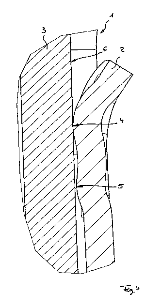
Fig. 4: shows an enlarged section (IV) from Fig. 3.
Figs. 1 to 4 show an embodiment of a system according to the invention
with a contact part 1 according to the invention with a plurality of contact
elements 2 which make contact with a mating contact element 3. The
system is used for the transmission of RF signals.
The contact part 1 according to the invention is designed in the form of a
spring cage. This is formed by a stamped and bent component with a
circular cross section in the wall of which the contact elements 2 are
integrated in the form of spring tabs.
The spring cage (or a base body thereof) consists of a metallic material, for
example phosphorus bronze. A coating for the base body can also be
provided which can, for example, be nickel-based and can improve the
contact resistance between the contact part 1 and the mating contact
element 3 in comparison with the phosphorus bronze.
The contact elements 2 each form a contact region at their free ends. Two
contact points 4, 5 are provided in each of these contact regions which are
formed by the outer side of a partially spherical section of the contact
element 2. These partially spherical sections can be introduced into the
contact elements 2 simply by means of a forming process.
When the mating contact element 3, in the form of a plug, is plugged into
the spring cage, the contact elements 2 are elastically deformed radially
outwards. As a consequence, the contact elements 2 press, in a spring-
loaded manner, against a contact surface 6 formed by the outer side of the
CA 02884269 2015-03-09
W02014/0406'70 6
PCT/EP2013/002159
mating contact element.
According to the invention, in the new state of the contact part 1 only a
first
contact point 4 arranged nearer to the free end of the relevant spring tab
makes contact with the contact surface 6. In contrast, a defined distance of
approx. 0.02 mm to 0.03 mm is provided between the respective second
contact point 5 and the contact surface 6 (see Fig. 4). In the new state,
therefore, only the first contact points 4 of the contact elements 2 are
responsible for the transmission of the RF signals from the contact part 1 to
the mating contact element 3.
If the system is subjected to continuous vibrations, i.e. vibratory stress, or
repeated plugging and disconnecting movements in which the contact part
1 is slid over the contact surface 6 of the mating contact element 3, this can
lead to wear on the first contact points 4 which in particular leads to a
(partial) erosion of the coating on the first contact points 4. This
increasing
wear leads to the second contact points 5 of the contact elements 2
approaching the contact surface 6 of the mating contact element 3 and
eventually making contact with this. This preferably happens shortly before
the coating has become completely eroded from the first contact points 4.
The coating, which is then present in its full thickness on the second contact
points 5 then ensures a continuing good transmission of the RE signals with
a relatively low contact resistance.
Naturally, it is also possible to provide more than two, for example three
contact points on some or all contact elements 2, wherein for example the
third contact points are, in the new state of the contact parts, preferably
arranged at the same distance from the second contact points 5 as the
second contact points 5 are distant from the first contact points 4.
It is also possible for several first (4) and several second (5) (and if
necessary several more) contact points to be provided per contact element
2.