Note: Descriptions are shown in the official language in which they were submitted.
CA 02884378 2015-03-09
DESCRIPTION
Title of Invention: OPTICAL MULTIPLEXING DEVICE
Technical Field
[0001]
The present invention relates to an optical multiplexing
device for multiplexing a plurality of lights.
Background Art
[0002]
In order that a plurality of lights emitted from a
plurality of laser light sources may be made incident on an
optical fiber, it is necessary to multiplex those plurality
of lights. Techniques for multiplexing lights are, for
example, disclosed in PTLs 1 and 2. According to the technique
disclosed in PTL 1, a plurality of waveguides are coupled at
their one ends so as to multiplex lights. On the other hand,
according to the technique disclosed in PTL 2, a plurality of
input-side optical fibers are welded with an output-side
optical fiber so as to multiplex lights.
[0003]
Another PTL 3 discloses an optical switch device as
follows. First, light incidence surfaces of a plurality of
optical fibers on which an output light may be incident are
1
CA 02884378 2015-03-09
aligned with one another. Then a parabolic mirror is slid in
parallel to those incidence surfaces so as to change over an
optical fiber on which the light should be incident.
[0004]
Further another PTL 4 discloses that a light emitted from
a light source is collimated using a reflection surface which
is a curved surface.
Citation List
Patent Literature
[0005]
PTL 1: JP-A-2006-330436
PTL 2: JP-A-2007-163650
PTL 3: JP-A-2008-145459
PTL 4: JP-A-2006-517675
Summary of Invention
Technical Problem
[0006]
The present inventor has investigated miniaturization
of an optical multiplexing device. That is, an object of the
present invention is to provide a small-sized optical
multiplexing device.
Solution to Problem
2
CA 02884378 2015-03-09
[0007]
According to the invention, an optical multiplexing
device includes a first optical fiber, a plurality of second
optical fibers, and a reflection surface. The second optical
fibers are disposed around the first optical fiber. One ends
of the second optical fibers are directed in the same direction
as one end of the first optical fiber. The reflection surface
is a parabolic surface, which faces the one end of the first
optical fiber and the one ends of the second optical fibers.
The one end of the first optical fiber is located on an axis
of the parabolic surface.
Advantageous Effects of Invention
[0008]
According to the invention, an optical multiplexing
device can be miniaturized.
Brief Description of Drawings
[0009]
The aforementioned object, other objects, features and
advantages will be made more obvious by preferred embodiments
which will be described below and the following drawings which
are attached to the embodiments.
[0010]
[Fig. 1] Fig. 1 is a sectional view showing the configuration
3
CA 02884378 2015-03-09
of an optical multiplexing device according to a first
embodiment.
[Fig. 2] Fig. 2 is a plan view for explaining the layout of
a first optical fiber and second optical fibers.
[Fig. 3] Fig. 3 is a view for explaining a use example of the
optical multiplexing device.
[Fig. 4] Fig. 4 is a sectional view showing the configuration
of an optical multiplexing device according to a second
embodiment.
[Fig. 5] Fig. 5 is a sectional view showing the configuration
of an optical multiplexing device according to a third
embodiment.
Description of Embodiments
[0011]
Embodiments of the invention will be described below with
reference to the drawings. Constituent parts similar to each
other among the drawings are referenced correspondingly, and
description thereof will be omitted accordingly.
[0012]
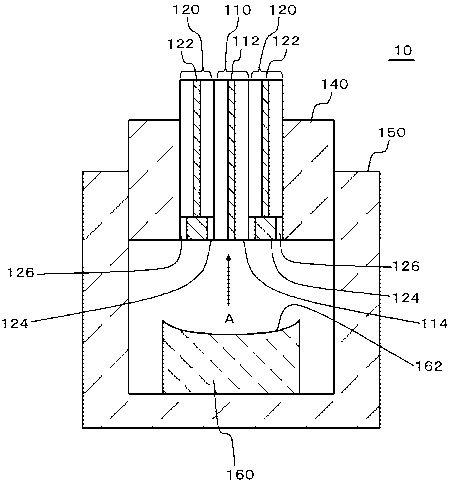
(First Embodiment)
Fig. 1 is a sectional view showing the configuration of
an optical multiplexing device 10 according to a first
embodiment. The optical multiplexing device 10 according to
the embodiment has a first optical fiber 110, a plurality of
4
CA 02884378 2015-03-09
second optical fibers 120, and a reflection surface 162. The
second optical fibers 120 are disposed around the first optical
fiber 110. One ends 124 of the second optical fibers 120 are
directed in the same direction as one end 114 of the first
optical fiber 110. The reflection surface 162 is a parabolic
surface, which faces the one end 114 and the one ends 124. In
addition, the one end 114 is located on an extension line of
an axis of the parabolic surface of the reflection surface 162,
that is, on an extension line of an axis of a parabolic line
serving as a base of the parabolic surface. Detailed
description will be made below.
[0013]
The first optical fiber 110 is provided for emitting a
light multiplexed in the optical multiplexing device 10. The
second optical fibers 120 are provided for making lights to
be multiplexed in the optical multiplexing device 10 incident
thereon. The first optical fiber 110 and the second optical
fibers 120 are, for example, single-mode fibers, each having
a core 112, 122. The first optical fiber 110 and the second
optical fibers 120 are not limited to the single-mode fibers
but may be multi-mode fibers. In addition, the one end 114
of the first optical fiber 110 and the one ends 124 of the second
optical fibers 120 form one and the same surface, for example,
one and the same flat surface. However, the one end 114 and
the one ends 124 do not have to form one and the same surface.
= CA 02884378 2015-03-09
[0014]
A collimator 126 is provided at the front end of each
second optical fiber 120. The one end 124 of the second optical
fiber 120 corresponds to an end surface of the collimator 126.
The collimator 126 collimates a light emitted from the second
optical fiber 120. When the second optical fiber 120 is a
single-mode fiber, the collimator 126 is formed by a graded
index type optical fiber welded with the second optical fiber
120. In the example shown in Fig. 1, the diameter of the second
optical fiber 120 and the diameter of the collimator 126 are
equal to each other. However, those diameters may be different
from each other.
[0015]
The first optical fiber 110 and the second optical fibers
120 are bundled using one and the same annular member 140 (for
example, ferrule) . That is, the first optical fiber 110 and
the second optical fibers 120 abut against one another. On
this occasion, the second optical fibers 120 are placed to
surround the first optical fiber 110. The first optical fiber
110 and the second optical fibers 120 are fixed to the inner
wall of the annular member 140, for example, by use of a bonding
agent.
[0016]
Incidentally, the one ends 114 and 124 of the first
optical fiber 110 and the second optical fibers 120 which have
6
CA 02884378 2015-03-09
been fixed into the annular member 140 are polished so that
the one ends 114 and 124 can be made flush with one other.
[0017]
The annular member 140 is inserted into a hollow
retention member 150. The retention member 150 has an optical
member 160 in a hollow portion thereof. The optical member
160 is disposed in, of the hollow portion of the retention
member 150, a position facing an opening portion to which the
annular member 140 is inserted. The surface of the optical
member 160 facing the opening portion becomes a reflection
surface 162. That is, when the annular member 140 is inserted
into the opening portion of the retention member 150, the one
end 114 of the first optical fiber 110 and the one ends 124
of the second optical fibers 120 face the reflection surface
162.
[0018]
The optical member 160 is formed, for example, out of
resin, glass or the like. A reflection film which can reflect
light is formed in the reflection surface 162. The reflection
film is, for example, a metal thin film such as an Al thin film,
but may be another film.
[0019]
As described above, the reflection surface 162 has a
parabolic surface. The reflection surface 162 is made into
a parabolic surface, for example, by polishing. An end portion
7
CA 02884378 2015-03-09
(a portion located in the one end 114) of the core 112 of the
first optical fiber 110 is disposed on an extension line of
an axis of the parabolic surface. This end portion preferably
coincides with a focal point of the reflection surface 162.
However, the end portion may be displaced from the focal point
of the reflection surface 162 to some extent.
[0020]
Fig. 2 is a plan view for explaining the layout of the
first optical fiber 110 and the second optical fibers 120. Fig.
2 corresponds to a view from the direction A in Fig. 1. In
the example shown in Fig. 2, that is, in a plane perpendicular
to the central axis of the reflection surface 162 which is a
parabolic surface, the second optical fibers 120 are disposed
on a circumference centering the core 112 of the first optical
fiber 110. In this manner, enlargement of the optical
multiplexing device 10 can be suppressed even if a plurality
of second optical fibers 120 are provided in the optical
multiplexing device 10. In the example shown in Fig. 2, the
first optical fiber 110 and the second optical fibers 120 have
the same diameter, and six second optical fibers 120 are
disposed around the first optical fibers 110. However, the
diameter of each second optical fiber 120 maybe different from
the diameter of the first optical fiber 110.
[0021]
Fig. 3 is a view for explaining a use example of the
8
CA 02884378 2015-03-09
=
optical multiplexing device 10. Lights from light sources 200
are incident on the second optical fibers 120 respectively.
Each light source 200 has, for example, a laser light source.
At least one light source 200 may further include a wavelength
conversion element. That is, the light sources 200 may emit
lights whose wavelengths coincide with one another, or at least
one light source 200 may emit a light whose wavelength is
different from those of the other light sources 200.
[0022]
As described above, the reflection surface 162 faces the
one ends 124 of the second optical fibers 120. Therefore,
lights entering the second optical fibers 120 from the light
sources 200 are emitted from the one ends 124 of the second
optical fibers 120 and applied onto the reflection surface 162.
The first optical fiber 110 is located on the extension line
of the axis of the parabolic surface of the reflection surface
162. Therefore, most of the lights reflected on the reflection
surface 162 enter the first optical fiber 110. In this manner,
all of the lights emitted from the light sources 200 are
multiplexed in the first optical fiber 110 and emitted to the
outside.
[0023]
Here, the position of the reflection surface 162 and the
positions of the second optical fibers 120 with respect to the
first optical fiber 110 are set so that the incident angles
9
CA 02884378 2015-03-09
of the lights in the one end 114 of the first optical fiber
110 can be made smaller than the critical angle of the core
112.
[0024]
Incidentally, when the collimators 126 are provided at
the front ends of the second optical fibers 120, the lights
emitted from the second optical fibers 120 are collimated.
Therefore, the lights can enter the first optical fiber 110
with high efficiency. In addition, when the first optical
fiber 110 is located at the focal point of the reflection
surface 162, the lights emitted from the second optical fibers
120 can enter the first optical fiber 110 with high efficiency.
[0025]
An apparatus provided with the light sources 200 and the
optical multiplexing device 10 is, for example, used as a light
source for an optical signal transmitting apparatus, a
spectroscopic measurement apparatus or a spectroscopic
analysis apparatus, a light source for a laser machining
apparatus, a light source fora laser microscope , alight source
for a DNA analysis apparatus, a light source for an endoscope,
or a light source for a funduscopy apparatus.
[0026]
According to the embodiment, as has been described, all
of the one end 114 of the first optical fiber 110 and the one
ends 124 of the second optical fibers 120 face the reflection
CA 02884378 2015-03-09
surface 162. The reflection surface 162 forms a parabolic
surface. The one end 114 is located on the extension line of
the axis of the parabolic surface of the reflection surface
162. Therefore, all of the lights emitted from the one ends
124 of the second optical fibers 120 enter the one end 114 of
the first optical fiber 110. Thus, a plurality of lights can
be multiplexed by use of the optical multiplexing device 10.
In addition, the optical multiplexing device can be constituted
by the first optical fiber 110, the second optical fibers 120
and the reflection surface 162. Thus, the optical
multiplexing device can be miniaturized.
[0027]
Further, the optical coupling system of the optical
multiplexing device 10 is formed out of a reflection optical
system. Accordingly, the optical coupling system may be
hardly affected by chromatic aberration when lights incident
on the second optical fibers 120 are in a visible light region,
for example, when the wavelengths of the lights are in a range
not shorter than 400 nm and not longer than 600 nm.
[0028]
(Second Embodiment)
Fig. 4 is a sectional view showing the configuration of
an optical multiplexing device 10 according to a second
embodiment. The optical multiplexing device 10 according to
the second embodiment has the same configuration as the optical
11
CA 02884378 2015-03-09
=
multiplexing device 10 according to the first embodiment,
except that the optical multiplexing device 10 according to
the second embodiment includes an antireflection film 170.
[0029]
The antireflection film 170 is provided on the one end
114 of the first optical fiber 110 and the one ends 124 of the
second optical fibers 120. In the example shown in Fig. 4,
the one end 114 and the one ends 124 form one and the same surface.
Therefore, the antireflection film 170 is formed as a
continuous film on the one end 114 and the one ends 124. The
antireflection film 170 is, for example, a dielectric film,
which is formed using a deposition method or the like.
[0030]
Also according to the embodiment, a similar effect to
that of the first embodiment can be obtained. In addition,
due to the antireflection film 170 formed on the one end 114
and the one ends 124, lights can be multiplexed with higher
efficiency.
[0031]
(Third Embodiment)
Fig. 5 is a sectional view showing the configuration of
an optical multiplexing device 10 according to a third
embodiment. The optical multiplexing device 10 according to
the third embodiment has the same configuration as the optical
multiplexing device 10 according to the first embodiment,
12
CA 02884378 2015-03-09
except for the following points.
[0032]
First, the optical member 160 is formed out of a
translucent material (such as glass or translucent resin).
The reflection surface 162 of the optical member 160 is formed
in, of the optical member 160, an opposite surface 164 to the
surface facing the first optical fiber 110 and the second
optical fibers 120. The surface 164 abuts against the one end
114 of the first optical fiber 110 and the one ends 124 of the
second optical fibers 120. Specifically, the surface 164 is
a flat surface, which abuts against the flat surface consisting
of the one end 114 and the one ends 124.
[0033]
Incidentally, the reflection surface 162 may be
processed into a parabolic surface after the optical member
160 is bonded to the first optical fiber 110 and the second
optical fibers 120. Alternatively, the optical member 160 may
be bonded to the first optical fiber 110 and the second optical
fibers 120 after the reflection surface 162 is processed into
a parabolic surface. In any case, a reflection film may be
formed on the reflection surface 162 at any timing as long as
the reflection surface 162 has been processed into a parabolic
surface.
[0034]
In the embodiment, lights emitted from the one ends 124
13
CA 02884378 2015-03-09
of the second optical fibers 120 are passed through the optical
member 160 and reflected on the reflection surface 162. The
reflected lights are passed through the optical member 160 and
incident on the first optical fiber 110.
[0035]
In this manner, also according to the embodiment, a
similar effect to that of the first embodiment can be obtained.
In addition, it will go well if the surface 164 of the optical
member 160 is attached to the one end 114 of the first optical
fiber 110 and the one ends 124 of the second optical fibers
120. Thus, the number of man-hours for manufacturing the
optical multiplexing device 10 can be reduced. Incidentally,
also in this embodiment, the antireflection film 170 may be
provided.
[0036]
The embodiments of the invention have been described
above with reference to the drawings. The embodiments
exemplify the invention, but various configurations other than
the aforementioned configurations may be used.
[0037]
The present application claims priority based on
Japanese Patent Application No. 2012-252933 filed on November
19, 2012, the contents of which will be incorporated herein
by reference.
14