Note: Descriptions are shown in the official language in which they were submitted.
- 1 -
DEVICE FOR USE IN THE DETECTION OF BINDING AFFINITIES
The present invention relates to a device for use in the
detection of binding affinities as well as a system for the
detection of binding affinities.
Such devices are used, for example, as biosensors in a
large variety of applications. One particular application is
the detection or monitoring of binding affinities or
processes. For example, with the aid of such biosensors
various assays detecting the binding of target samples to
binding sites can be performed. Typically, large numbers of
such assays are performed on a biosensor at spots which are
arranged in a two-dimensional microarray on the surface of
the biosensor. The use of microarrays provides a tool for the
simultaneous detection of the binding affinities or processes
of different target samples in high-throughput screenings,
wherein large numbers of target samples like molecules,
proteins or DNA can be analysed quickly. For detecting the
affinities of target samples to bind to specific binding
sites (e.g. the affinities of target molecules to bind to
different capture molecules), a large number of binding sites
are immobilised on the surface of the biosensor at spots
which can be applied, for instance, by ink-jet spotting or
photolithography. Each spot forms an individual measurement
zone for a predetermined type of capture molecules. The
affinity of a target sample to a specific type of capture
molecules is detected and is used to provide information on
the binding affinity of the target sample.
CA 2884694 2020-03-10
CA 02884694 2015-009
WO 2014/086789 PCT/EP2013/075408
- 2 -
A known technique for detecting binding affinities of
target samples uses labels which are capable of emitting
fluorescent light upon excitation. For example, fluorescent
tags can be used as labels for labelling the target samples.
Upon excitation, the fluorescent tags are caused to emit
fluorescent light having a characteristic emission spectrum.
The detection of this characteristic emission spectrum at a
particular spot indicates that the labelled target molecule
has bound to the particular type of binding sites present at
the respective spot.
A sensor for detecting labelled target samples is
described in the article "Zeptosens' protein microarrays: A
novel high performance microarray platform for low abundance
protein analysis", Proteomics 2002, 2, S. 383-393, Wiley-VCH
Verlag GmbH, 69451 Weinheim, Germany. The sensor described
there comprises a planar waveguide arranged on a substrate,
and a grating for coupling coherent light of a predetermined
wavelength into the planar waveguide. A further grating is
arranged at that end of the planar waveguide remote from the
grating for coupling the light into the waveguide. Coherent
light that has propagated through the planar waveguide is
coupled out of the waveguide by the further grating. The
outcoupled light is used for adjustment of the coupling of
coherent light of predetermined wavelength into the planar
waveguide. The coherent light propagates through the planar
waveguide under total reflection with an evanescent field of
the coherent light propagating along the outer surface of the
planar waveguide. The depth of penetration of the evanescent
field into the medium of lower refractive index at the outer
surface of the planar waveguide is in the order of magnitude
of a fraction of the wavelength of the coherent light
CA 028846 94 2015-03-09
WO 2014/086789 PCT/EP2013/075408
- 3 -
pr op agating through the planar waveguide. The evanescent
field excites the fluorescent tags of the labelled target
samples bound to the binding sites arranged on the surface of
the planar waveguide. Due to the very small penetration of
the evanescent field into the optically thinner medium at the
outer surface of the planar waveguide, only the labelled
samples bound to the binding sites immobilized on the outer
surface of the planar waveguide are excited. The fluorescent
light emitted by these tags is then detected with the aid of
a CCD camera.
While it is principally possible to detect the binding
affinities using fluorescent labels, this technique is
disadvantageous in that the detected signal is produced by
the labels rather than by the binding partners themselves. In
addition, labelling the target samples requires additional
working steps. Moreover, labelled target samples are
comparatively expensive. Another disadvantage is the
falsification of the results caused by steric hindrance of
the fluorescent labels at the target sample which might
interfere with the binding of the target samples to the
capture molecules. Further disadvantages are the
falsification of the results due to photobleaching of the
labels or quenching effects.
It is an object of the present invention to provide a
device for use in the detection of binding affinities of a
target sample as well as a system capable of detecting such
binding affinities which overcome or at least greatly reduce
the disadvantages of the prior art sensor described above.
CA 028846 94 2015-03-09
WO 2014/086789 PCT/EP2013/075408
- 4 -
In accordance with the invention, this object is
achieved by a device for use in the detection of binding
affinities. The device comprises a planar waveguide arranged
on a substrate, and further comprises an optical coupler of a
predetermined length for coupling coherent light of a
predetermined wavelength into the planar waveguide such that
a parallel beam of coherent light propagates through the
planar waveguide with an evanescent field of the coherent
light propagating along an outer surface of the planar
waveguide. The outer surface of the planar waveguide
comprises binding sites thereon capable of binding target
samples to the binding sites such that light of the
evanescent field is diffracted by target samples bound to the
binding sites. The binding sites are arranged along a
plurality of predetermined straight lines running parallel to
one another with a constant distance between adjacent
straight lines. The predetermined straight lines are arranged
at an angle 13 relative to the direction of propagation of the
evanescent field such that the coherent light diffracted by
the target samples bound to the binding sites impinges under
a diffraction angle a relative to the straight lines onto a
further optical coupler arranged in a portion of the planar
waveguide outside the beam of coherent light propagating
through the planar waveguide. The further optical coupler
couples the diffracted coherent light out of the planar
waveguide such as to interfere at a predetermined detection
location with a difference in optical path length which is an
integer multiple of the predetermined wavelength.
Technically, the term "diffracted" describes the interference
of the coherent light of the evanescent field which already
has interacted with target samples bound to the binding
sites. The diffraction causes the coherent light propagating
CA 02884694 2015-009
WO 2014/086789 PCT/EP2013/075408
- 5 -
through the planar waveguide with an evanescent field at the
outer surface to constructively interfere under predetermined
directions within the planar waveguide.
The detection of binding affinities according to the
invention is neither limited to specific types of target
samples nor to any type of binding sites, but rather the
binding characteristics of molecules, proteins, DNA etc. can
be analysed with respect to any type of binding sites on the
planar waveguide. The detection of binding affinities can be
achieved in a label-free manner. Alternatively, diffraction
enhancers (e.g. diffracting labels) which strongly scatter
the light can be used to increase the detection sensitivity.
Such diffraction enhancers can be a nanoparticle (alone or
with a binder) or in another example a colloidal particle.
Advantageously, the binding characteristic to be analysed can
be of static type (for example, it can be analysed whether a
target sample has or has not bound to the binding sites) or
of dynamic type (for example, the dynamics of the binding
process over time can be analysed). According to the
invention the device comprises a planar waveguide on a
substrate, the planar waveguide having a high refractive
index relative to the medium on the outer surface forming the
upper side of the planar waveguide. For example, the
refractive index of the planar waveguide may be in the range
of 1.6 to 2.8, whereas the refractive index of the medium at
the surface of the planar waveguide is typically in the range
of 1 to 1.6, in particular 1.33 - 1.4 for water or aqueous
assay buffer and 1 for air. The effective refractive index N
of the guided mode, the refractive index of the medium at the
surface of the planar waveguide and the predetermined
wavelength of the light determine the penetration depth
CA 02884694 2()15-()09
WO 2014/086789 PCT/EP2013/075408
- 6 -
(distance between the outer surface of the planar waveguide
and the 1/e2 intensity descent of the evanescent field) of
the evanescent field into the medium on the outer surface of
the planar waveguide. The penetration depth is such that the
evanescent field penetrating out of the outer surface of the
planar waveguide is diffracted at the target samples bound to
the binding sites arranged at the outer surface. In use,
coherent light of a predetermined wavelength (which is
preferably monochromatic) is coupled via an optical coupler
into the planar waveguide such that a parallel beam of
coherent light propagates through the planar waveguide with
the evanescent field propagating along the outer surface. The
parallel beam has a width corresponding to the predetermined
length of the optical coupler which is in case of an optical
grating for coupling coherent light into the planar waveguide
the length of the lines defining the optical grating. The
predetermined wavelength is not limited to specific values
but is rather preferred to be in the range of visible light.
The outer surface of the planar waveguide comprises binding
sites thereon. Binding sites are locations on the outer
surface of the planar waveguide to which a target sample may
bind. For example, binding sites may comprise capture
molecules which are immobilized on the outer surface of the
planar waveguide, or may simply comprise activated locations
on the outer surface of the planar waveguide which are
capable of binding target samples to the activated locations,
or may be embodied in any other manner suitable to bind
target samples at the desired locations on the outer surface
of the planar waveguide. In principle, binding sites being
capable of binding target samples such that light of the
evanescent field is diffracted by target samples bound to the
binding sites. According to the invention, the binding sites
CA 02884694 2015-009
WO 2014/086789 PCT/EP2013/075408
- 7 -
are arranged along a plurality of predetermined straight
lines. The arrangement of the binding sites "along the
predetermined straight lines" represents the optimum case in
which all binding sites are exactly arranged on the
predetermined straight lines. Such optimal arrangement of the
binding sites results in a maximum signal at the detection
location. It is obvious to the person skilled in the art that
in practice the arrangement of the binding sites can deviate
to some extent from such optimum arrangement without losing a
detectable signal in the detection location. For example, the
deviation may be caused by the respective method for
arranging the binding sites on the outer surface of the
planar waveguide, as will be explained in detail below. The
straight lines are such that light diffracted thereto
constructively interferes in a maximum of high intensity
within the planar waveguide. The predetermined straight lines
run parallel to one another with a constant distance between
adjacent straight lines. Preferred constant distances between
adjacent predetermined straight lines are of the order of
more than 100 nm. For the distance between adjacent
predetermined lines a range of about 100 nm to about 1000 nm,
in particular between 300 nm - 600 nm is preferred. The
mentioned ranges allow the use of visible, near infrared and
soft UV light of which the wavelength ranges from 350 nm to
1500 nm so that the diffracted light can be detected by
standard optical means. The predetermined straight lines are
arranged at an angle [3 in the range of 10 to 70 relative to
the direction of propagation of the evanescent field. The
direction of propagation is defined as starting from the
optical coupler and extending in the direction in which the
coherent light is coupled into the planar waveguide which is
usually close to perpendicular to the lines of the optical
CA 02884694 2015-009
WO 2014/086789 PCT/EP2013/075408
- 8 -
grating which form the optical coupler. The coherent light
diffracted by the target samples bound to the binding sites
impinges onto the further optical coupler under the
diffraction angle a relative to the straight lines. The
diffraction angle under which the light constructively
interferes by an integer multiple of the predetermined
wavelength depends on the constant distance between adjacent
predetermined straight lines taking into account the
predetermined wavelength and the refractive indices of the
substrate, the planar waveguide and of the medium at the
outer surface of the waveguide at this wavelength. Since the
light of the evanescent field propagating along the outer
surface of the planar waveguide is coherent as is the light
propagating through the planar waveguide, the coherent light
of the evanescent field is diffracted coherently by the
diffraction centers formed by the target samples bound to the
binding sites which are arranged on the different
predetermined straight lines. The diffracted light at any
location can be determined by adding the contributions from
each of the individual diffraction centers. Advantageously,
the internal diffraction of the light propagating through the
planar waveguide is of a higher efficiency compared to the
diffraction of the guided light out of the planar waveguide.
Since the diffraction at the target samples bound to binding
sites is usually rather weak, the diffraction within the
plane of the planar waveguide provides an improved detection
sensitivity which even allows detecting comparatively small
numbers of diffraction centers. The further optical coupler
onto which the diffracted light impinges can be a physical
grating suitable to couple the light out of the planar
waveguide. A further crucial point of the Invention is that
the further optical coupler is arranged in a portion of the
CA 028846 94 2015-03-09
WO 2014/086789 PCT/EP2013/075408
- 9 -
planar waveguide outside the beam of coherent light
propagating through the planar waveguide. This allows
detecting the signal from the diffracted light without a
background from the beam of coherent light propagating
through the planar waveguide. Because of the signal detected
in the detection location has less background signal, a
better detection sensitivity is achieved which allows to
detect a signal caused by less diffraction centers. A maximum
of the diffracted light is located at the predetermined
detection location because the further optical coupler is
formed as a grating such that at the predetermined detection
location, the optical path length of the light diffracted by
the different lines of the grating differs by an integer
multiple of the wavelength of the light. For a maximum signal
at the detection location, the optical path length of the
light from the optical coupler to the predetermined straight
lines, from there to the further optical coupler and from
there to the predetermined detection location is also a
multiple integer of the predetermined wavelength. Thus the
light diffracted by the target samples bound to the binding
sites constructively interferes at a predetermined detection
location. The requirement of constructive interference is met
by the diffracted light which adds to the detectable signal
in the detection location.
According to an advantageous aspect of the invention,
the constant distance d between the adjacent straight lines
is chosen such as to fulfill the Bragg condition
2Ndsin(o)=kA, wherein N is the effective refractive index of
the guided mode in the planar waveguide, d is the distance
between adjacent predetermined straight lines, a is the
diffraction angle, k is the number of the intensity maximum
CA 028846 94 2015-03-09
WO 2014/086789 PCT/EP2013/075408
- 10 -
and A is the vacuum wavelength of the propagating light. It
is important to note that the distance between adjacent
predetermined straight lines d at which constructive
interference at a predetermined detection location occurs
depends on the effective refractive index N which - in turn -
depends on the refractive index of the medium at the outer
surface of the waveguide. Advantageously, the distance
between adjacent predetermined straight lines d is chosen to
factor in the change in refractive index for different
samples applied to the outer surface. A constant distance d
between adjacent lines explicitly includes small changes in
the distance between adjacent lines. Such gradient in the
distance between adjacent lines over the plurality of
predetermined lines allows fulfilling the Bragg condition in
only a fraction of the plurality of predetermined lines.
According to another advantageous aspect of the
invention, the predetermined straight lines are arranged at
the angle p in the range of 10 -70 relative to the direction
of propagation of the evanescent field. The coherent light
diffracted by the target samples bound to the binding sites
impinges under the diffraction angle cx (which equals p)
relative to the straight lines onto the further optical
coupler. Arranging the predetermined straight lines and the
further optical coupler at fixed angles is of advantage for
the preparation of the predetermined straight lines on the
outer surface of the device, which have a fixed orientation
thereon.
According to a further advantageous aspect of the
invention, the further optical coupler comprises a plurality
CA 028846 94 2015-03-09
WO 2014/086789 PCT/EP2013/075408
- 11 -
of grating lines. Each of the plurality of grating lines has
a respective curvature and distance between adjacent grating
lines so that the further optical coupler is capable of
coupling the diffracted coherent light out of the planar
waveguide such as to interfere at a predetermined detection
location with a difference in optical path length which is an
integer multiple of the predetermined wavelength. The
plurality of grating lines may have a symmetry axis which
extends relative to the predetermined straight lines under
the diffraction angle oc. This symmetry perseveres to a
plurality of grating lines in the further optical coupler
with a symmetric curved grid-like structure of a decreasing
distance between adjacent grating lines so that light of a
single predetermined wavelength coupled out of the planar
waveguide fulfills the condition that the difference in
optical path length is a multiple integer of the single
predetermined wavelength in the detection location. To
arrange the symmetry axis under the diffraction angle allows
the detection location to include the central axis of the
circular formed optical grating.
According to a still further advantageous aspect of the
invention, the plurality of predetermined straight lines is
arranged in an effective zone on the planar waveguide. The
effective zone has a width equivalent to the length of the
optical coupler so that the entire effective zone is
illuminated by the evanescent field of the coherent light
coupled into the planar waveguide by the optical coupler. The
beam propagating in the waveguide has a small angle of
divergence so that the increase of beam-width compared to the
other dimensions of the device is negligible. Thus the width
of the effective zone can generally be chosen identical to
CA 02884694 2015-009
WO 2014/086789 PCT/EP2013/075408
- 12 -
the length of the optical coupler for illuminating the entire
effective zone. In practice however, the width of the
effective zone is smaller compared to the length of the
optical coupler. As an example, the width of the effective
zone is 310 pm while the length of the optical coupler is 400
pm.
According to another advantageous aspect of the
invention, at least two pluralities of predetermined straight
lines are arranged on the planar waveguide one after the
other in the direction of propagation of the evanescent
field. A respective further optical coupler is arranged
relative to each plurality of predetermined straight lines
such that the coherent light diffracted by the target samples
bound to the binding sites arranged along the straight lines
of the respective plurality of straight lines impinges under
a diffraction angle a onto the respective further optical
coupler. By arranging the pluralities of predetermined
straight lines one after the other in the direction of
propagation of the evanescent field, the evanescent field of
the beam impinges onto (diffracts at) all pluralities of
predetermined straight lines arranged in such manner so as to
allow the simultaneous detection of binding affinities in a
multitude of samples.
In a preferred alternative aspect of the invention, the
at least two pluralities of predetermined straight lines each
have the same constant distance d between adjacent straight
lines. The same constant distance d between adjacent straight
lines of each plurality of predetermined straight lines
allows a redundant detection of binding affinities in a
CA 028846 94 2015-03-09
WO 2014/086789 PCT/EP2013/075408
- 13 -
multitude of samples.
In a further preferred alternative aspect of the
invention, the at least two pluralities of predetermined
straight lines each have a different constant distance c11...õ
between adjacent straight lines. The different constant
distance di., may cover a range of constant distances which
corresponds to a range of detectable refractive indices in
the medium at the outer surface of the waveguide. The range
of detectable refractive indices allows detecting binding
affinities for samples in media with different or unknown
refractive indices. The refractive index in the samples that
are brought into contact with the sensor surface might vary
in the range of a few per cents due to different composition.
In a preferred additional aspect of the invention, the
constant distance d1. between adjacent straight lines of
adjacent pluralities of predetermined straight lines differs,
in steps of 0.5 to 3 nm. Having pluralities of predetermined
straight lines with a difference in constant distance
which changes in equal steps allows to conveniently quantify
binding affinities in samples of different or unknown
refractive indices in the range of known detectable
refractive indices. Constructive interference at a
predetermined detection location occurs when the distance d
of the plurality of predetermined straight lines matches the
Bragg condition for the refractive index of the applied
sample.
In a still further preferred alternative aspect of the
invention, the at least two pluralities of predetermined
straight lines include groups of pluralities of predetermined
CA 02884694 2015-009
WO 2014/086789 PCT/EP2013/075408
- 14 -
straight lines, each group having an equal constant distance
d between adjacent straight lines. Different groups of
pluralities of predetermined straight lines have a different
constant distance dln between adjacent straight lines. Having
groups of equal constant distance d between adjacent straight
lines combines the advantages discussed for the other
alternatives so as to allow the redundant detection of
binding affinities as well as to detect binding affinities
for samples in media with different or unknown refractive
indices in the range of known detectable refractive indices.
In a still further preferred aspect of the invention,
the optical coupler comprises at least two separate portions
for coupling coherent light of the predetermined wavelength
into the planar waveguide. Each separate portion has a
predetermined length and is separated by a predetermined
spacing towards the other separate portion such that at least
two parallel beams of coherent light propagate through the
planar waveguide separated by the predetermined spacing. The
separate portions of the optical coupler allow arranging one
or more pluralities of predetermined straight lines in the
direction of propagation of each beam coupled via the
respective separate portion into the planar waveguide. By
separating the parallel beams coupled to the waveguide with a
predetermined spacing in between causes a portion of the
planar waveguide outside the parallel beams of coherent
light. The further optical coupler arranged in said portion
improves the detected signal by reducing the background light
in the detection location. In an example for the further
optical coupler having a size of 400 pm, the predetermined
spacing is chosen to be 600 pm.
CA 02884694 2015-009
WO 2014/086789 PCT/EP2013/075408
- 15 -
According to an advantageous aspect of the invention,
the binding sites comprise capture molecules attached to the
outer surface of the planar waveguide along the predetermined
straight lines only. The capture molecules are capable of
binding the target samples. Two embodiments are particularly
envisaged of how the binding sites can be arranged along the
plurality of predetermined straight lines. According to a
first embodiment, the binding sites comprise capture
molecules attached to the surface of the planar waveguide
along the predetermined lines only. These capture molecules
are capable of binding the target samples and are immobilized
on the outer surface of the planar waveguide (although, as
mentioned above, the binding sites can be formed by the
activated surface of the planar waveguide itself).
Immobilizing the capture molecules on the outer surface of
the planar waveguide along the predetermined lines can
generally be performed by any suitable method, for example it
may be performed using photolithographic methods using a
lithographic mask with straight lines. It goes without
saying, that the arrangement of the binding sites along the
predetermined straight lines is to be understood in any
embodiment of the invention in a sense that the majority of
the binding sites - in the instant embodiment the capture
molecules - are located along the predetermined straight
lines and does explicitly include that some binding sites are
arranged at locations different therefrom.
According to the second embodiment, the binding sites
comprise capture molecules capable of binding the target
samples, the capture molecules capable of binding the target
samples being arranged along the predetermined straight lines
by immobilization of the capture molecules capable of binding
CA 02884694 2015-009
WO 2014/086789 PCT/EP2013/075408
- 16 -
the target samples onto the outer surface of the planar
waveguide and by deactivation those capture molecules which
are not arranged along the predetermined straight lines. The
term "deactivation" in this respect refers to any suitable
method for changing the binding capability of the capture
molecules before or after their immobilization on the outer
surface of the planar waveguide. The deactivation can be
achieved, for example, by exposing the capture molecules to
UV light in order to achieve that they are no longer capable
of binding target samples. The deactivation of the capture
molecules immobilized between the predetermined straight
lines can be achieved, for example, by an alteration of the
binding region of the capture molecule. According to this
embodiment of the invention, the capture molecules can be
applied uniformly or statistically uniformly onto the outer
surface of the planar waveguide. After deactivation of
capture molecules which are arranged between the
predetermined straight lines only the capture molecules
arranged along the predetermined straight lines (these have
not been deactivated) are capable of binding a target sample.
Nevertheless, the deactivated capture molecules remain
immobilized on the outer surface of the planar waveguide.
This embodiment has the additional advantage that the
contribution of the signal generated by the light diffracted
by target molecules bound to capture molecules to the overall
signal at the detection location is increased. Generally, the
difference between the signals of the light diffracted by
small target molecules bound to the captures molecules and
the light diffracted by the capture molecules without any
target molecules bound thereto is small compared to the light
diffracted by the capture molecules alone. Assuming that the
CA 02884694 2015-009
WO 2014/086789 PCT/EP2013/075408
- 17 -
diffraction properties of the capture molecules arranged
along the predetermined straight lines (which have not been
deactivated) and of the deactivated capture molecules
arranged between the predetermined straight lines are nearly
identical and further assuming that the capture molecules are
homogeneously distributed over the outer surface of the
planar waveguide, then ideally no signal is produced at the
detection location after the capture molecules have been
immobilized on the outer surface of the planar waveguide and
after the capture molecules arranged between the
predetermined straight lines have been deactivated. In
practice, however, deactivation of the capture molecules
slightly changes the diffraction properties of the capture
molecules, so that it may not be ideal to deactivate all of
the capture molecules which are arranged between the
predetermined straight lines. Instead, only the vast majority
of the capture molecules arranged between the predetermined
straight lines may be deactivated. Deactivation of the
capture molecules is performed to an extent such that the
overall signal at the detection location produced by those
capture molecules arranged along the predetermined straight
lines and by those deactivated and the non-deactivated
capture molecules arranged between the predetermined straight
lines is at a minimum, and is preferably zero. Assuming that
the signal so obtained at the detection location can be
reduced to zero, this means, that after adding the target
samples the signal produced at the detection location only
results from target samples bound to the capture molecules.
In case no target samples are bound to the capture molecules,
the signal at the detection location remains zero. This
increases the sensitivity of the detector for the signal
generated by the light diffracted by the target molecules
- 18 -
bound to the capture molecules at the detection location.
Another aspect of the invention relates to a system for
the detection of binding affinities comprising a device
according to any one of the foregoing aspects, and further
comprising a light source for emitting coherent light of a
predetermined wavelength. The light source and the device are
arranged relative to one another such that the coherent light
emitted by the light source is coupled into the planar
waveguide via the optical coupler.
According to an additional aspect of the invention, the
light source and the device are arranged adjustable relative
to each other for changing the incoupling angle under which
the coherent light emitted by the light source is coupled via
the optical coupler into the planar waveguide. The light
source emits coherent light of a predetermined wavelength,
preferentially in the visible, near infrared or soft UV
spectral range with a (tunable) wavelength in the range from
350 nm to 1500 nm.
According to a further aspect of the invention, the light
source is tunable to emit coherent light of predetermined
wavelength with a tuning range of about 1 to 5 nm. The tuning
range of the light source allows arranging the light source
and the device at a fixed incoupling angle. The light emitted
by the tunable light source is coupled via an optical coupler
(e.g. optical grating) into the planar waveguide when the
wavelength of the emitted light in the tuning range matches
the wavelength at which coupling occurs at the fixed
incoupling angle.
CA 2884694 2020-03-10
CA 02884694 2015-009
WO 2014/086789 PCT/EP2013/075408
- 19 -
The tunable light source can be used for a second
advantageous mode of operation of the device in a system for
the detection of binding affinities. The Bragg condition
describing the maximum intensity of constructive interference
relates the distance between adjacent predetermined straight
lines, the angle under which the evanescent field is
diffracted at the target samples bound to the binding sites
which are arranged along the predetermined straight lines,
the wavelength of the light propagating through the planar
waveguide and the effective refractive index N of the guided
mode. Considering samples of which the refractive index is
not exactly known, the tunable light source allows to vary
the wavelength at which coupling occurs such that the Bragg
condition for the maximum intensity of constructive
interference is fulfilled (even for a fixed distance between
adjacent lines and a fixed diffraction angle relative to the
predetermined lines). The variation of both, the wavelength
of the tunable light source and the incoupling angle (under
which the light is coupled via the optical coupler into the
waveguide) allows to adjust the wavelength at which coupling
into the waveguide occurs to the wavelength which fulfills
the Bragg condition for a fixed distance between adjacent
predetermined straight lines.
Further advantageous aspects of the invention become
apparent from the following description of an embodiment of
the device with reference to the accompanying drawings in
which:
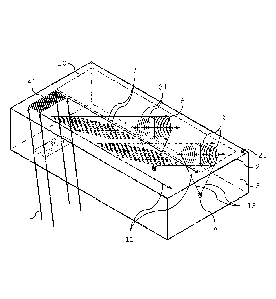
Fig. 1 shows a perspective view of a first embodiment
of the device according to the invention;
CA 02884694 2015-03-09
WO 2014/086789 PCT/EP2013/075408
- 20 -
Fig. 2 shows a plan view of the planar waveguide of
the device of Fig. 1 illustrating different
angles according to the invention;
Fig. 3 shows a plan view of the planar waveguide of
the device of Fig. 1 illustrating the
arrangement of the binding sites;
Fig. 4 shows a plan view of the planar waveguide of
the device of Fig. 1 illustrating an effective
zone;
Fig. 5 shows a plan view of the planar waveguide of
the device of Fig. 1 illustrating different
optical paths;
Fig. 6 shows a plan view of the planar waveguide of
the device of Fig. 1 having two pluralities of
predetermined straight lines;
Fig. 7 shows three pluralities of predetermined lines
having a difference in constant distance d
between adjacent predetermined straight lines;
Fig. 8 shows a plan view of a mask to be used for
preparation of a device according to a second
embodiment of the invention having the pattern
of 24 pluralities of predetermined straight
lines thereon;
CA 02884694 2015-03-09
WO 2014/086789 PCT/EP2013/075408
- 21 -
Fig. 9 shows a plan view of a non-prepared device
according to the second embodiment of the
invention to be prepared with the mask of Fig.
8;
Fig. 10 shows a plan view of the prepared device
according to the second embodiment of the
invention which is the device of Fig. 9 ready
for use in the detection of binding
affinities;
Fig. 11 shows a schematic illustration visualizing the
difference in optical path length for the
diffraction of the light of the evanescent
field on target samples bound to binding sites
arranged along the plurality of predetermined
straight lines;
Fig. 12 shows the schematic illustration of Fig. 11
with binding sites comprising capture
molecules along a plurality of predetermined
straight lines and in between deactivated
capture molecules for achieving a minimum
background signal; and
Fig. 13 shows the schematic illustration of Fig. 12
with the target samples applied to the capture
molecules capable of binding.
Fig. 1 shows a perspective view of an embodiment of the
CA 02884694 2015-009
WO 2014/086789 PCT/EP2013/075408
- 22 -
device for use in the detection of binding affinities.
Structurally, the device comprises a substrate 3, a plurality
of predetermined straight lines 7 (each of the shown lines
represent a multiplicity of lines) arranged on an outer
surface 21 of a planar waveguide 2, an optical coupler 41, a
detection location and a further optical coupler 8. It is
further shown that according to the working principle of the
device, the coherent light 1 is coupled into the planar
waveguide 2 so as to propagate with an evanescent field 11
(represented by parallel arrows) which is diffracted so that
diffracted coherent light 12 (represented by parallel arrows)
propagates under an angle relative to the predetermined lines
7 to be coupled out of the planar waveguide 2 such that
coupled light 13 coupled out of the planar waveguide 2
interferes in the detection location 9.
In the shown example, the planar waveguide 2 is arranged
on the substrate 3 which both allow visible coherent light to
propagate therethrough. Since the planar waveguide 2 has a
thickness in the range of some ten nanometers to some hundred
nanometers it is drawn together with the line of the top
surface from substrate 3. The coherent light 1 provided by a
light source (not shown) has a predetermined wavelength. In
practice, the predetermined wavelength is not limited to
specific values for the wavelength but rather is to be chosen
inter alia according to the effective refractive index of the
guided mode as well as to the size, position and geometry of
the optical coupler 41, the predetermined lines 7 and the
further optical coupler 8. For coupling the coherent light 1
of a predetermined wavelength into the planar waveguide 2,
the optical coupler 41 employs in the shown example a grating
with straight lines of a predetermined length so as to allow
CA 028846 94 2015-03-09
WO 2014/086789 PCT/EP2013/075408
- 23 -
coherent coupling of the coherent light 1 under a
predetermined coupling angle into the planar waveguide 2.
Because of the predetermined length of the coupler 41 a
parallel beam of coherent light having a width according to
the length of the optical coupler 41 propagates through the
planar waveguide 2. The parallel beam of coherent light has
an evanescent field 11 of a characteristic penetration depth.
The penetration depth of the evanescent field 11 into the
medium on the outer surface 21 of the planar waveguide 2
(distance between the outer surface 21 of the planar
waveguide 2 and the 1/e2 intensity descent of the evanescent
field 11) depends on the effective refractive index N of the
guided mode, on the refractive index of the medium at the
surface of the planar waveguide and on the wavelength A of
the light. The light of the evanescent field 11 is diffracted
by target samples (not shown in Fig. 1) bound to the binding
sites (not shown in Fig. 1). In principle, the binding sites
are arranged along the plurality of predetermined straight
lines 7 which run parallel to one another with a constant
distance between adjacent straight lines. The predetermined
straight lines 7 are arranged on the outer surface 21 of the
planar waveguide 2 at an angle relative to the direction of
propagation of the evanescent field 11. The light of the
evanescent field 11 is diffracted so as to impinge under a
diffraction angle relative to the straight lines onto a
further optical coupler 8 formed in the planar waveguide 2.
The diffracted light interferes in the further optical
coupler 8 with a difference in optical path length of a
multiple integer of the predetermined wavelength.
Advantageously, the internal diffraction of the light
propagating through the planar waveguide 2 is of a higher
efficiency compared to the diffraction of the guided light
CA 02884694 2015-009
WO 2014/086789 PCT/EP2013/075408
- 24 -
out of the planar waveguide 2. This provides a sufficient
detection sensitivity which allows detecting comparatively
small numbers of diffraction centers. In theory, there might
he other diffraction angles relative to the straight lines
having a maximum intensity of the diffracted light so that
the further optical coupler 8 can be arranged at other
diffraction angles, as well. A further advantage of the
invention can be seen from Fig. 1 with respect to the
arrangement of the further optical coupler 8. The further
optical coupler 8 and thus the detection location 9 are
arranged on the planar waveguide 2 and oriented relative to
each other such that no light of the beam propagating through
the planar waveguide 2 is detected. Thus, the further optical
coupler 8 is arranged in a portion 10 of the planar waveguide
2 outside the beam of coherent light propagating through the
planar waveguide 2 starting from the optical coupler 41. This
allows detecting the signal from the diffracted light without
a background from the beam of coherent light propagating
through the planar waveguide. A still further advantage
relates to the signal detected in the detection location 9
having less background signal because of the location of the
further optical coupler 8 in the portion 10. Thus, a better
detection sensitivity is achieved which allows to detect a
signal caused by less diffraction centers. The further
optical coupler 8 is shown to be a phase grating lens
oriented with the axis of symmetry in the direction of the
diffraction angle. The phase grating lens exemplifies any
optical means to couple the diffracted coherent light 12 out
of the planar waveguide 2 while focusing it in the detection
location 9 with a sufficient intensity for the detection of
binding affinities.
CA 02884694 2015-03-09
WO 2014/086789 PCT/EP2013/075408
- 25 -
Figs. 2-6, respectively, are plan views of the outer
surface 21 of the planar waveguide 2 from Fig. 1 which
already describes the planar waveguide 2, the optical coupler
41, the further optical coupler 8 and the plurality of
predetermined lines 7 arranged on the outer surface 21 of the
planar waveguide 2.
In Fig. 2 the angle a relative to the predetermined
straight lines 7 and the angle p relative to the direction of
propagation of the evanescent field 11 are illustrated. In
the present embodiment the angle p is 22.5 and the angle a
is 22.5 . The fixed angles are obviously of advantage for the
preparation of the device. The evanescent field 11
(represented by an arrow starting from the optical coupler 41
and ending in the center of the predetermined straight lines
7) propagating along the outer surface 21 of the planar
waveguide 2 diffracts on target samples (not shown) bound to
binding sites (not shown). The diffracted coherent light 12
(represented by an arrow starting from the center of the
predetermined straight lines 7 and propagating along the
symmetry axis of the further optical coupler 8)
constructively interferes such as to impinge under the angle
a of 22.5 onto the further optical coupler 8. The angle a is
according to the Bragg condition 2Ndsin(a)=kX dependent from
the distance d between adjacent predetermined straight lines
7 and from the predetermined wavelength A and can be varied
to fulfill the Bragg condition. N is the effective refractive
index of the guided mode in the planar waveguide and A is the
vacuum wavelength of the light propagating through the planar
waveguide 2.
CA 02884694 2015-009
WO 2014/086789 PCT/EP2013/075408
- 26 -
A plan view of the planar waveguide 2 of the device of
Fig. 1 with an exaggerated illustration of the binding sites
arranged along predetermined straight lines 7 is provided
in Fig. 3. In the exaggerated illustration, the light of the
5 evanescent field 11 is represented by parallel arrows
approaching the predetermined straight lines 7, which are
arranged under a known angle 3 thereto. The predetermined
straight lines 7 are arranged parallel to one another with a
constant distance d. The diffracted coherent light 12
diffracted on the target samples 6 bound to the binding sites
5 arranged along the predetermined straight lines 7 has for
predetermined angles a difference in optical path length
which is a multiple integer of the wavelength. The diffracted
coherent light 12 has for those predetermined angles a
maximum intensity. The described diffraction angle is the
first angle under which such a maximum in intensity occurs.
In fact this is the well-known drawing depicting the
principle of Bragg diffraction in which the light is
diffracted at "crystal structures" to constructively
interfere in certain directions. This illustration is not
correct insofar as the binding sites 5 and in this way the
target samples 6 bound to the binding sites 5 are not
arranged along the predetermined straight lines 7 in the
shown regular order. The arrangement of those deviate to some
extend in both, along those lines and perpendicular to those
lines without losing the intensity maximum of the diffracted
coherent light 12.
In Fig. 4 the arrangement of the predetermined straight
lines 7 in an effective zone 71 on the planar waveguide 2 is
explanatorily depicted. The construction of the effective
zone 71 is shown with respect to the coherent light
CA 028846 94 2015-03-09
WO 2014/086789 PCT/EP2013/075408
- 27 -
propagating through the planar waveguide 2. Assuming a
uniform density of diffraction centers in the effective zone
71, in principle, the bigger the area of the effective zone
71, the more diffraction centers will contribute to the
diffracted coherent light 12. The area of the effective zone
71 is primarily chosen in dependence on the strength of the
detected signal to be suitable for detecting the binding
affinities. Since the length of the optical coupler 41 is
fixed, the width of the effective zone 71 is fixed to be
equivalent thereto. This allows illuminating the entire
effective zone 71 by the evanescent field 11, as shown by the
parallel arrows laterally confining the width of the
effective zone 71. The length of the effective zone 71 is
such that at one hand the diffracted coherent light 12
impinges entirely on the further optical coupler 8 while on
the other hand the further optical coupler 8 is only
illuminated by the diffracted coherent light 12 from
diffraction centers in the effective zone 11. The lateral
separation of diffracted coherent light 12 from the
evanescent field 11 restricts the light impinging on the
further optical coupler 8 to diffracted coherent light 12
from diffraction centers in the effective zone 71 and avoids
additional background light in the region 10 through which -
apart from the diffracted light 12 - no other light
propagates.
In Fig. 5 two examples for different optical paths of
light are illustrated by the arrows for the evanescent field
11, the arrows for diffracted coherent light 12 as well as
for the light 13 interfering in the detection location 9. In
principle, a multiplicity of parallel beams start at the
optical coupler 41 to diffract over the entire area of the
CA 02884694 2015-009
WO 2014/086789 PCT/EP2013/075408
- 28 -
effective zone 71 in which the predetermined straight lines 7
are arranged. The diffracted coherent light 12 propagates
towards the further optical coupler 8 with difference in
optical path of a multiple integer of the predetermined
wavelength. The diffracted coherent light 12 impinges on the
further optical coupler 8 such as to be coupled out of the
planar waveguide 2. The further optical coupler 8 is depicted
as optical grating with a plurality of grating lines 81. The
grating lines 81 are formed such that the diffracted coherent
light 12 impinging thereon is coupled out of the planar
waveguide 2 and is focused into the detection location 9. For
focusing the light 13 coupled out of the planar waveguide
into the detection location 9, each of the plurality of
grating lines 81 has a respective curvature and the lines are
arranged with a decreasing distance between adjacent grating
lines 81 in the direction of propagation of the diffracted
coherent light 12. This allows diffraction of light of a
predetermined wavelength "ideally" into a single point of
focus with a difference in optical path length which is a
multiple integer of the predetermined wavelength. A blank
section 82 is formed in the further optical coupler 8 to
avoid a 2nd order Bragg reflection, or similar optical
effects, which potentially decrease the overall intensity of
the detected signal.
One advantageous aspect of the present invention is
shown in Fig. 6, wherein the planar waveguide 2 of the device
of Fig. 1 comprises two pluralities of predetermined straight
lines 7. The two pluralities of predetermined straight lines
7 have a different distance between adjacent predetermined
straight lines 7. In general, the different distance between
adjacent predetermined straight lines 7 allows the detection
CA 02884694 2015-009
WO 2014/086789 PCT/EP2013/075408
- 29 -
of binding affinities for samples having a different
refractive index under the same "fixed" diffraction angle.
Each different refractive index of the sample causes a
different effective refractive index for the light
propagating through the planar waveguide 2. Generally, the
effective refractive index of the guided mode in the planar
waveguide depends on the thickness and the refractive index
of the planar waveguide 2, the refractive index of the
substrate, the refractive index of a medium on the outer
surface 21 of the planar waveguide 2 and the polarization of
the guided mode. Thus, the evanescent field 11 of the light
propagating through the planar waveguide 2 has different
specific optical path length between adjacent lines for
different samples on the waveguide. In practice, the
refractive index of the medium on the outer surface 21 of the
planar waveguide 2 is not exactly known. Advantageously, the
plurality of predetermined straight lines 7 with different
distances allow to detect a signal for an unknown refractive
index in a range of known detectable refractive indices which
might vary in the second or third decimal of the refractive
index from sample to sample. For the detection of binding
affinities it is sufficient if a single plurality of
predetermined straight lines 7 shows a detectable signal. As
shown, the at least two pluralities of predetermined straight
lines 7 are arranged on the planar waveguide 2 in the
direction of propagation of the evanescent field 11. The
coherent light 12 coupled into the planar waveguide 2 is
diffracted by the target samples 6 bound to the binding sites
5 of each plurality of predetermined straight lines 7. A
further optical coupler 8 is provided at each plurality of
predetermined straight lines V for light impinging under a
diffraction angle relative to the straight lines in a region
CA 028846 94 2015-03-09
WO 2014/086789 PCT/EP2013/075408
- 30 -
outside the beam of coherent light.
Fig. 7 refers again to the idea to arrange at least two
pluralities of predetermined straight lines 7 at the planar
waveguide 2. This is illustrated by the arrangement of three
5 pluralities of predetermined lines 7 with the plurality on
the left side marked as having a first constant distance d1_24
between adjacent straight lines 7 out of a number of 24
constant distances. This refers to the idea that 24
pluralities of predetermined straight lines 7 are arranged
10 each having a different constant distance d between adjacent
straight lines. As an example, the distance d1 between
adjacent predetermined lines is 446 nm and the distance d2
between adjacent predetermined lines is 447 nm. 24
pluralities of predetermined straight lines is an arbitrarily
chosen number which provides in the present example a range
of 24 different distances between 446 nm to 469 nm in steps
of 1 nm. The mentioned steps provide a range sufficient to
cover the expected variation of effective refractive indices
in the second or third decimal (corresponding to an effective
refractive index variation in the per cent to per mule
range).
A second embodiment of the invention is provided in the
device shown in Figs. 9 and 10, which depict the device
before preparation, as well as, when readily prepared for
use. Said device is prepared with the mask 14 shown in Fig.
8.
Fig. 8 shows the mask 14 for use in a photolithographic
method for arranging the binding sites 5 to the outer surface
CA 02884694 2015-009
WO 2014/086789 PCT/EP2013/075408
- 31 -
21 of the planar waveguide 2 along the predetermined straight
lines 7. Such a mask 14 comprises a pattern thereon suitable
to transfer predetermined straight lines 7 on the outer
surface 21. The pattern is used in photolithographic
procedures to attach the binding sites in predetermined
straight lines 7 on the outer surface 21 of the planar
waveguide 2. The not yet prepared device is shown in Fig. 9.
Photolithographic methods exemplify any suitable method for
arranging the predetermined straight lines 7 at the outer
surface 21 of the planar waveguide 2. In general every method
known in the art suitable to structure binding sites on the
nanometer to micrometer scale can be employed to arrange the
binding sites thereon. In Fig. 10 the prepared device is
shown with 24 pluralities of predetermined straight lines 7.
The 24 pluralities of predetermined straight lines 7 are
arranged in a line with respect to one of the three separate
portions 411, 412, 413 so that the coherent light coupled via
each of said separate portions diffracts on eight pluralities
of predetermined straight lines 7 arranged one after the
other. The 24 pluralities of predetermined straight lines 7
are arranged in three parallel rows having a distance in
between which forms a portion 10 of the planar waveguide 2
outside the parallel beams of coherent light propagating
through the planar waveguide. The optical coupler 41
comprises three separate portions 411, 412, 413 for coupling
three parallel beams of coherent light into the planar
waveguide 2. The three separate portions 411, 412, 413
forming the optical coupler are arranged in a row and being
laterally spaced by a predetermined distance from the
adjacent separate portion. Thus the parallel beams of
coherent light propagate through the planar waveguide 2
separated by this predetermined distance. Each separate
CA 02884694 2015-009
WO 2014/086789 PCT/EP2013/075408
- 32 -
portion 411, 412, 413 has a predetermined length equal to the
width of the plurality of predetermined straight lines 7
arranged in a single row of pluralities. Each separate
portion 411, 412, 413 couples a beam of coherent light into
the planar waveguide. In between are three portions 10 on the
outer surface 21 of the planar waveguide 2 which are outside
the beams of coherent light. The portions 10 are used to
arrange the further optical coupler 8 respectively to each
plurality of predetermined straight lines 7. The coherent
light which is not diffracted by the target samples bound to
the binding sites arranged along the predetermined straight
lines 7 propagates through the planar waveguide to the still
further optical coupler 42 for coupling out the light
propagating through the planar waveguide 2 which is not
diffracted at the target samples bound to the binding sites
arranged along the predetermined straight lines 7.
Fig. 11, Fig. 12 and Fig. 13 illustrate examples for the
diffraction of the light of the evanescent field 11. The
light 11 is diffracted at the target samples 6 bound to the
binding sites 5 arranged along predetermined lines 7 of a
distance d so as to contribute to a maximum in a
predetermined detection location. The shown illustrations are
well known from the description of Bragg diffraction in
"crystal structures". In principle, the Bragg condition
2Ndsin(o)=kA describes the angles under which a maximum
intensity of diffracted light can be detected. Due to the
parallel arrangement of the predetermined straight lines 7 at
a constant distance d between adjacent lines, the light of
the evanescent field 11 diffracted on subsequent lines
interferes under predetermined diffraction angles so as to
have a difference in optical path length of a multiple
CA 02884694 2015-009
WO 2014/086789 PCT/EP2013/075408
- 33 -
integer of the predetermined wavelength of the light
propagating through the planar waveguide 2. Thus, the shown
parallel beams 12 of the diffracted light interfere at those
diffraction angles so as to have a difference in optical path
length of a integer multiple of the predetermined wavelength
of the propagating light. The shown samples exemplify target
samples 6 bound to binding sites without any precondition to
the type of binding sites as well as the type of target
samples 6. For the constructive interference it is crucial to
arrange the binding sites to which the target samples may
bind, or not, along the predetermined straight lines 7 so
that the light constructively interferes under the prescribed
conditions.
In Fig. 11, the binding sites comprise a single type of
capture molecules. The detection of binding affinities tests
the capability of capture molecules to bind target samples 6,
or not, by actually observing the binding of the target
samples 6 to the capture molecules. The capture molecules are
in this first example attached to the outer surface of the
planar waveguide to be arranged along the predetermined
straight lines 7 only.
According to another example shown in Fig. 12 and Fig.
13, the capture molecules 5 capable of binding the target
samples 6 being arranged along the predetermined straight
lines 7 by arranging capture molecules 5 capable of binding
the target samples 6 onto the entire outer surface of the
planar waveguide and by deactivating those capture molecules
51 which are not arranged along the predetermined straight
lines 7.
CA 02884694 2015-009
WO 2014/086789 PCT/EP2013/075408
- 34 -
This is achieved by that the capture molecules are
immobilised over the (entire) outer surface of the planar
waveguide, so that there is no arrangement of the capture
molecules along the plurality of predetermined lines 7 only.
Thus, the light of the evanescent field 11 diffracted by the
capture molecules 5 and the capture molecules 51 does not
interfere at the further optical coupler in the manner
described above for the diffracted coherent light 12.
Subsequently, the capture molecules 51 arranged between
the predetermined lines 7 are deactivated so that no target
samples 6 can bind to these deactivated capture molecules 51
anymore. As shown in Fig. 12, deactivation is performed such
that after deactivation the overall signal at the further
optical coupler (no target samples 6 have been added yet)
produced by the deactivated capture molecules 51 and the
capture molecules 5 capable of binding the target samples is
set or adjusted to a tuned minimum signal (so as to
destructively interfere) at the detection location, ideally
to zero. The light 121 diffracted at the deactivated capture
molecules 51 as well as at the capture molecules 5 has a
difference in optical path length so as to add to a minimum
in a predetermined detection location. The shown lines of
capture molecules 5 and deactivated capture molecules 51 are
"ideal" lines but provide a sufficient approximation since
the light diffracted from capture molecules 5 and deactivated
capture molecules 51 arranged other than (or in the proximity
of) the plurality of predetermined "ideal" lines 7 in
principle eliminates itself.
Alternatively, the minimum signal before the application
CA 02884694 2015-009
WO 2014/086789 PCT/EP2013/075408
- 35 -
of the target samples can be achieved by that capture
molecules 5 and deactivated capture molecules 51 are
subsequently applied so that in a first step the capture
molecules 5 are applied to the outer surface of the planar
waveguide along the plurality of predetermined straight lines
7 (comparable to Fig. 11). In a subsequent step, deactivated
capture molecules 51 are applied in between the lines of the
plurality of predetermined straight lines 7.
In the last step, the target samples are added to the
outer surface of the planar waveguide. Since only the capture
molecules arranged along the predetermined lines 7 are
capable of binding the target samples 6, the target samples 6
bind to those capture molecules along the predetermined lines
7, as this is shown in Fig. 13. Due to the signal at the
detection location caused by the deactivated capture
molecules 51 and the capture molecules has been set or
adjusted to a minimum before (see Fig. 12), the signal at the
detection location is then mainly (or entirely, if the signal
produced by deactivated capture molecules 51 and the capture
molecules 5 has been reduced to zero before) caused by the
light 12 which has been diffracted by the target samples 6
bound to the capture molecules arranged along the
predetermined lines 7.
While the embodiments of the invention have been
described with the aid of the drawings, various modifications
and changes to the described embodiments are possible without
departing from the general teaching underlying the invention.
Therefore, the invention is not to be understood as being
limited to the described embodiments, but rather the scope of
CA 02884694 2015-03-09
WO 2014/086789
PCT/EP2013/075408
- 36 -
protection is defined by the claims.