Note: Descriptions are shown in the official language in which they were submitted.
CA 02884779 2015-03-11
1
Pane with an Electrical Connection Element
The invention relates to a pane with an electrical connection element, an
economical and
environmentally friendly method for its production, and its use.
The invention relates in particular to a pane with an electrical connection
element for motor
vehicles with electrically conductive structures such as, for instance,
heating conductors or
antenna conductors. The electrically conductive structures are customarily
connected to the
onboard electrical system via soldered-on electrical connection elements. Due
to different
coefficients of thermal expansion of the materials used, mechanical stresses
occur during
production and operation that strain the panes and can cause breakage of the
pane.
Lead-containing solders have high ductility that can compensate the mechanical
stresses
occurring between an electrical connection element and the pane by plastic
deformation.
However, because of the End of Life Vehicles Directive 2000/53/EC, lead-
containing solders
have to be replaced by lead-free solders within the EC. The directive is
referred to, in
summary, by the acronym ELV (End of Life Vehicles). Its objective is to ban
extremely
problematic components from products resulting from the massive increase in
disposable
electronics. The substances affected are lead, mercury, and cadmium. This
relates, among
other things, to the implementation of lead-free soldering materials in
electrical applications
on glass and the introduction of corresponding replacement products.
A number of electrical connection elements for leadfree soldering to
electrically conductive
structures have been proposed. Reference is made, by way of example, to the
documents
US 20070224842 Al, EP 1942703 A2, WO 2007110610 Al, EP 1488972 Al, and
EP 2365730 Al. The shape of the connection element, on the one hand, and the
material of
the connection element, on the other, assume critical significance with regard
to the
avoidance of thermal stresses.
The object of the present invention is to provide a pane with an electrical
connection element
that is particularly suited for soldering using leadfree solder materials,
wherein critical
mechanical stresses in the pane are avoided. Moreover, an economical and
environmentally
friendly method for their production is to be provided.
CA 02884779 2015-03-11
2
The object of the present invention is accomplished according to the invention
by a pane
with at least one electrical connection element according to the independent
claim 1.
Preferred embodiments emerge from the subclaims.
The pane according to the invention with at least one electrical connection
element
comprises at least the following characteristics:
- a substrate,
- on a region of the substrate, an electrically conductive structure,
- on a region of the electrically conductive structure, a connection element
that includes at
least a chromium-containing steel,
wherein the connection element has a region crimped around a connection cable
and a
solder region and wherein the solder region is connected to the electrically
conductive
structure via a leadfree solder material.
According to the invention, the electrical connection element is connected to
the connection
cable by crimping. The crimp connection is simple, economical, and quick to
produce and
can be readily automated. Costly additional process steps, for example,
soldering or welding
the connection element to the connection cable can be avoided. At the same
time, a very
stable connection between the connection element and the connection cable is
provided.
The connection element according to the invention with the crimped region (the
so-called
crimp, i.e., the region deformed by the crimping procedure) can be produced
simply and
economically and enables space-saving, flexibly usable, and durably stable
electrical
contacting of the electrically conductive structure.
Chromium-containing, in particular so-called "stainless steel" or "corrosion
resistant steel"
steel is available economically. Connection elements made of chromium-
containing steel
also have high rigidity in comparison to many conventional connection
elements, made, for
example, of copper, which results in an advantageous stability of the crimped
connection.
Chromium-containing steel has good cold formability, because of which it is
particularly
suited for production of crimp connections. In addition, compared to many
conventional
connection elements, for example, those made of titanium, chromium-containing
steel has
improved solderability, due to higher thermal conductivity.
The connection cable is provided to electrically connect the electrically
conductive structure
to an external functional element, for example, a power supply or a receiver.
For this, the
connection cable is guided away from the pane starting from the connection
element
CA 02884779 2015-03-11
3
preferably beyond the side edges of the pane. The connection cable can, in
principle, be any
connection cable that is known to the person skilled in the art for the
electrical contacting of
an electrically conductive structure and is suitable for being connected by
crimping to the
connection element (also called "crimp contact"). The connection cable can
include, in
addition to an electrically conductive core (inner conductor), an insulating,
preferably
polymer sheathing, with the insulating sheathing preferably removed in the end
region of the
connection cable to enable an electrically conductive connection between the
connection
element and the inner conductor.
The electrically conductive core of the connection cable can, for example,
include copper,
aluminum, and/or silver or alloys or mixtures thereof. The electrically
conductive core can,
for example, be implemented as a stranded wire conductor or as a solid wire
conductor. The
cross-section of the electrically conductive core of the connection cable
depends on the
current-carrying capacity required for the application of the pane according
to the invention
and can be selected appropriately by the person skilled in the art. The cross-
section is, for
example, from 0.3 mm2 to 6 mm2.
The connection element, which includes, according to the invention, at least a
chromium-
containing steel and is preferably made from the chromium-containing steel, is
preferably
crimped in the end region of the connection cable around the electrically
conductiven core of
the connection cable such that a durably stable electrically conductive
connection is
developed between the connection element and the connection cable. The
crimping is done
with a suitable crimping tool, known per se to the person skilled in the art,
for example,
crimping pliers or a crimping press. Customarily, the crimping tool comprises
two active
points, for example, the jaws of crimping pliers, which are guided against
each other, by
which means mechanical pressure is exerted on the connection element. The
connection
element is thus plastically deformed and squeezed around the connection
element.
In a preferred embodiment of the electrical connection element according to
the invention,
the solder region is disposed on the side of the crimped region which faces
the extension
direction of the connection cable to the external function element. The angle
between the
solder region and the crimped region is preferably from 120 to 180 ,
particularly preferably
from 1500 to 170 . By this means, a particularly space-saving and stable
electrical
contacting of the electrically conductive structure can be obtained.
CA 02884779 2015-03-11
4
The surface of the solder region facing the substrate forms the contact
surface between the
connection element and the electrically conductive structure and is connected
to the
electrically conductive structure via the solder material. Here, this means a
direct,
mechanical connection between the solder region and the electrically
conductive structure
via the solder material. This means that the solder material is disposed
between the solder
region and the electrically conductive structure and thus fixes the solder
region durably
stably on the electrically conductive structure.
In the solder region and in the crimped region, the connection element
preferably has the
same material thickness. This is particularly advantageous with regard to
simple production
of the connection element, since the connection element can be punched from a
single
sheet of metal. The material thickness of the connection element is preferably
from 0.1 mm
to 2 mm, particularly preferably from 0.2 mm to 1 mm, very particularly
preferably from 0.3
mm to 0.5 mm. In this range for the material thickness, the connection element
has, on the
one hand, the cold formability necessary for the crimping. On the other hand,
in this range
for the material thickness, an advantageous stability of the crimped
connection and an
advantageous electrical connection between the electrically conductive
structure and the
connection cable are obtained.
The length and the width of the solder region are preferably from 1 mm to 10
mm,
particularly preferably from 2 mm to 8 mm, and very particularly preferably
from 2.5 mm to 5
mm. This is particularly advantageous in view of a small space requirement of
the
connection element and effective electrical contacting of the electrically
conductive structure.
In a preferred embodiment, the solder region is implemented flat, which yields
a flat contact
surface. However, the solder region can also have regions introduced by
reshaping, such as
stamping or deep drawing, for example, solder depots, spacers, or contact
bumps. Apart
from the reshaped regions, the contact surface is preferably flat.
The shape of the solder region and of the contact surface can be selected
according to the
requirements in the individual case and can, for example, be polygonal,
rectangular,
rectangular with rounded corners, oval, elliptical, or circular.
The length of the crimped region can be appropriately selected by the person
skilled in the
art taking into account the diameter of the connection cable as well as
applicable standards
and is, for example, from 2 mm to 8 mm or from 4 mm to 5 mm, in particular 4.5
mm. This is
CA 02884779 2015-03-11
particularly advantageous in view of a small space requirement of the
connection element
and a stable connection between the connection element and the connection
cable.
Preferably, the crimp is implemented as an open crimp. Since, in this case,
the connection
cable does not have to be inserted into an all-around closed wire-end ferrule
(closed crimp),
such a crimp connection is easier to produce and can be readily automated and
is,
consequently, particularly suited for mass production. The shape of the crimp
can be freely
selected, for example, as a B-crimp or an 0-crimp.
The solder region can be connected directly to the crimped region of the
connection
element. However, a transition region, for example, with a length of 1 mm to 5
mm can be
disposed between the solder region and the crimped region. By means of a
transition region,
the flexibility in the design of the connection element is increased.
In addition to the crimped region, one or a plurality of other regions can be
connected to the
solder region. For example, another region can be disposed on the side edge of
the solder
region opposite the crimped region. Such another region can, for example, be
provided to
connect the connection element to a mounting bracket. For example, by means of
a shared
mounting bracket, a plurality of connection elements according to the
invention can be
soldered to the electrically conductive structure in a defined relative
arrangement.
In an advantageous embodiment, the pane has from two to six electrical
connection
elements according to the invention. By means of multiple connection elements,
an
electrically conductive structure implemented as a heating conductor can, for
example, be
connected to the two terminals of an external power supply. By means of
multiple
connection elements, different antennas applied on the substrate as
electrically conductive
structures can, for example, be contacted. Due to the small dimensions and
reduction of
thermal stresses, connection elements according to the invention are
particularly suited for
panes on which multiple connection elements can be disposed, even with little
distance
between them. The connection elements are preferably disposed in a line. The
distance
between adjacent connection elements is preferably from 5 mm to 50 mm,
particularly
preferably from 10 mm to 20 mm. This arrangement is advantageous from a
production
technology standpoint and for aesthetic reasons. In particular, the connection
elements in
this relative arrangement can be fixed, for example, before soldering in a
shared mounting
bracket. The side edges of the soldering regions of the different connection
elements are
preferably disposed parallel to each other and can have, relative to the
(imaginary) line on
which the connection elements are disposed, any angle, preferably from 5 to
90 ,
CA 02884779 2015-03-11
6
particularly preferably from 100 to 400. The crimped regions of the different
connection
elements are preferably disposed on the same side of the (imaginary) line.
Such an
arrangement is particularly space-saving.
The substrate has a first coefficient of thermal expansion. The connection
element has a
second coefficient of thermal expansion. In an advantageous embodiment of the
invention,
the difference between the first and the second coefficient of thermal
expansion is less than
x 10-6/0C, particularly preferably less than 3 x 10-61 C. Because of this, the
thermal
stresses in the pane are reduced and better adhesion is obtained.
The substrate contains, preferably, glass, particularly preferably flat glass,
float glass, quartz
glass, borosilicate glass, and/or soda lime glass. However, the substrate can
also contain
polymers, preferably polyethylene, polypropylene, polycarbonate, polymethyl
methacrylate,
polystyrene, polybutadiene, polynitriles, polyester, polyurethane, polyvinyl
chloride,
polyacrylate, polyamide, polyethylene terephthalate, and/or copolymers or
mixtures thereof.
The substrate is preferably transparent. The substrate preferably has a
thickness from
0.5 mm to 25 mm, particularly preferably from 1 mm to 10 mm, and very
particularly
preferably from 1.5 mm to 5 mm.
The first coefficient of thermal expansion is preferably from 8 x 10⁻⁶/ C to
9 x 10⁻⁶/ C. The substrate preferably contains glass that has, preferably, a
coefficient of
thermal expansion from 8.3 x 10⁻⁶/ C to 9 x 10⁻⁶/ C in a temperature range
from 0 C to
300 C.
The second coefficient of thermal expansion is preferably from 9 x 10⁻⁶/ C to
13 x 10-61 C, particularly preferably from 10 x 10-6/ C to 11.5 x 10-61 C,
very particularly
preferably from 10 x 10-6/ C to 11 x 10-6/ C, and in particular from 10 x 10-
6/ C to
10.5 x 10⁻⁶/ C in a temperature range from 0 C to 300 C.
The connection element according to the invention preferably includes a
chromium-
containing steel with a chromium proportion greater than or equal to 10.5 wt.-
%. Other alloy
components such as molybdenum, manganese, or niobium result in an improved
corrosion
resistance or altered mechanical properties, such as tensile strength or cold
formability.
The connection element according to the invention preferably includes at least
66.5 wt.-% to
89.5 wt.-% iron, 10.5 wt.-% to 20 wt.-% chromium, 0 wt.-% to 1 wt.-% carbon, 0
wt.-% to
CA 02884779 2015-03-11
7
wt-% nickel, 0 wt.-% to 2 wt.-% manganese, 0 wt.-% to 2.5 wt.-% molybdenum, 0
wt.-% to
2 wt.-% niobium, and 0 wt.-% to 1 wt.-% titanium. The connection element can
also include
admixtures of other elements, including vanadium, aluminum, and nitrogen.
The connection element according to the invention particularly preferably
includes at least
73 wt.-% to 89.5 wt.-% iron, 10.5 wt.-% to 20 wt.-% chromium, 0 wt.-% to 0.5
wt.-% carbon,
0 wt.-% to 2.5 wt.-% nickel, 0 wt.-% to 1 wt.-% manganese, 0 wt.-% to 1.5 wt.-
%
molybdenum, 0 wt.-% to 1 wt.-% niobium, and 0 wt.-% to 1 wt.-% titanium. The
connection
element can also include admixtures of other elements, including vanadium,
aluminum, and
nitrogen.
The connection element according to the invention very particularly preferably
includes at
least 77 wt.-% to 84 wt.-% iron, 16 wt.-% to 18.5 wt.-% chromium, 0 wt.-% to
0.1 wt.-%
carbon, 0 wt.-% to 1 wt.-% manganese, 0 wt.-% to 1 wt.-% niobium, 0 wt.-% to
1.5 wt.-%
molybdenum, and 0 wt.-% to 1 wt.-% titanium. The connection element can also
include
admixtures of other elements, including vanadium, aluminum, and nitrogen.
Particularly suitable chrome-containing steels are steels of the material
numbers 1.4016,
1.4113, 1.4509, and 1.4510 in accordance with EN 10 088-2.
The electrically conductive structure according to the invention has,
preferably, a layer
thickness from 5 pm to 40 pm, particularly preferably from 5 pm to 20 pm, very
particularly
preferably, from 8 pm to 15 pm, and, in particular, from 10 pm to 12 pm. The
electrically
conductive structure according to the invention contains, preferably, silver,
particularly
preferably, silver particles and glass frits.
The layer thickness of the solder material is preferably less than or equal to
6.0 x 10⁻⁴ m,
particularly preferably less than 3.0 x 10⁻⁴ m.
The solder material according to the invention is leadfree. This is
particularly advantageous
in view of the environmental impact of the pane with an electrical connection
element
according to the invention. In the context of the invention, "leadfree solder
material" means a
solder material that includes, in accordance with EC Directive "2002/95/EC on
the
Restriction of the Use of Certain Hazardous Substances in Electrical and
Electronic
Equipment", a lead proportion less than or equal to 0.1 wt.-%, preferably no
lead.
CA 02884779 2015-03-11
8
Leadfree solder materials typically have less ductility than lead-containing
solder materials,
such that mechanical stresses between a connection element and a pane can be
less well
compensated. However, it has been demonstrated that critical mechanical
stresses can
clearly be prevented by means of the connection element according to the
invention. The
solder material according to the invention contains, preferably, tin and
bismuth, indium, zinc,
copper, silver, or compositions thereof. The proportion of tin in the solder
composition
according to the invention is from 3 wt.-% to 99.5 wt.-%, preferably from 10
wt.-% to
95.5 wt.-%, particularly preferably from 15 wt.-% to 60 wt.-%. The proportion
of bismuth,
indium, zinc, copper, silver, or compositions thereof in the solder
composition according to
the invention is from 0.5 wt.-% to 97 wt.-%, preferably 10 wt.-% to 67 wt.-%,
whereby the
proportion of bismuth, indium, zinc, copper, or silver can be 0 wt.-%. The
solder composition
can contain nickel, germanium, aluminum, or phosphorus at a proportion of 0
wt.-% to
wt.-%. The solder composition according to the invention contains, very
particularly
preferably, Bi40Sn57Ag3, Sn40Bi57Ag3, Bi59Sn40Ag 1, Bi57Sn42Ag 1, 1n97Ag3,
Sn95.5Ag3.8Cu0,7, Bi67In33, Bi331n50Sn17, Sn77.21n20Ag2.8, Sn95Ag4Cu1,
Sn99Cu1,
Sn96.5Ag3.5, Sn96.5Ag3Cu0.5, Sn97Ag3, or mixtures thereof.
In an advantageous embodiment, the solder material contains bismuth. It has
been
demonstrated that a bismuth-containing solder material results in particularly
good adhesion
of the connection element according to the invention to the pane, by means of
which
damage to the pane can be avoided. The proportion of bismuth in the solder
material
composition is preferably from 0.5 wt.-% to 97 wt.-%, particularly preferably
10 wt.-% to
67 wt.-%, and very particularly preferably from 33 wt.-% to 67 wt.-%, in
particular from
50 wt.-% to 60 wt.-%. In addition to bismuth, the solder material preferably
contains tin and
silver or tin, silver, and copper. In a particularly preferred embodiment, the
solder material
includes at least 35 wt.-% to 69 wt.-% bismuth, 30 wt.-% to 50 wt.-% tin, 1
wt.-% to 10 wt.-%
silver, and 0 wt.-% to 5 wt.-% copper. In a very particularly preferred
embodiment, the solder
material contains at least 49 wt.-% to 60 wt.-% bismuth, 39 wt.-% to 42 wt.-%
tin, 1 wt.-% to
4 wt.-% silver, and 0 wt.-% to 3 wt.-% copper.
In another advantageous embodiment, the solder material contains from 90 wt.-%
to 99.5
wt.-% tin, preferably from 95 wt.-% to 99 wt.-%, particularly preferably from
93 wt.-% to 98
wt.-%. In addition to tin, the solder material preferably contains from 0.5
wt.-% to 5 wt.-%
silver and from 0 wt.-% to 5 wt.-% copper.
CA 02884779 2015-03-11
9
The solder material flows out with an outflow width of less than 1 mm from the
intermediate
space between the solder region of the connection element and the electrically
conductive
structure. In a preferred embodiment, the maximum outflow width is less than
0.5 mm and,
in particular, roughly 0 mm. This is particularly advantageous with regard to
the reduction of
mechanical stresses in the pane, the adhesion of the connection element, and
the reduction
in the amount of solder. The maximum outflow width is defined as the distance
between the
outer edges of the solder region and the point of the solder material
crossover, at which the
solder material drops below a layer thickness of 50 pm. The maximum outflow
width is
measured on the solidified solder material after the soldering process. A
desired maximum
outflow width is obtained through a suitable selection of solder material
volume and vertical
distance between the connection element and the electrically conductive
structure, which
can be determined by simple experiments. The vertical distance between the
connection
element and the electrically conductive structure can be predefined by an
appropriate
process tool, for example, a tool with an integrated spacer. The maximum
outflow width can
even be negative, i.e., pulled back into the intermediate space formed by the
solder region of
the electrical connection element and an electrically conductive structure. In
an
advantageous embodiment of the pane according to the invention, the maximum
outflow
width is pulled back in a concave meniscus into the intermediate space formed
by the solder
region of the electrical connection element and the electrically conductive
structure. A
concave meniscus is created, for example, by increasing the vertical distance
between the
spacer and the conductive structure during the soldering process, while the
solder is still
fluid. The advantage resides in the reduction of mechanical stresses in the
pane, in
particular, in the critical region present with a large solder material
crossover.
In an advantageous embodiment of the invention, the contact surface of the
connection
element has spacers, preferably at least two spacers, particularly preferably
at least three
spacers. The spacers are disposed on the contact surface between the
connection element
and the solder material and are preferably formed in one piece with the
connection element,
for example, by stamping or deep drawing. The spacers preferably have a width
of
0.5 x 10⁻⁴ m to 10 x 10-4 m and a height of 0.5 x 10⁻⁴ m to 5 x 10⁻⁴ m,
particularly preferably
of 10-4 m to 3 x 10⁻⁴ m. By means of the spacers, a homogeneous, uniformly
thick, and
uniformly fused layer of the solder material is obtained. Thus, mechanical
stresses between
the connection element and the pane can be reduced and the adhesion of the
connection
element can be improved. This is particularly advantageous with the use of
leadfree solder
materials that can compensate mechanical stresses less well due to their lower
ductility
compared to lead-containing solder materials.
CA 02884779 2015-03-11
In an advantageous embodiment of the invention, at least one contact bump,
which serves
for contacting the connection element with the soldering tool during the
soldering process, is
disposed on the surface of the solder region of the connection element facing
away from the
substrate. The contact bump is preferably curved convexly at least in the
region of
contacting with the soldering tool. The contact bump preferably has a height
of 0.1 mm to 2
mm, particularly preferably of 0.2 mm to 1 mm. The length and width of the
contact bump is
preferably between 0.1 and 5 mm, very particularly preferably between 0.4 mm
and 3 mm.
The contact bumps are preferably implemented in one piece with the connection
element,
for example, by stamping or deep drawing. For the soldering, electrodes whose
contact side
is flat can be used. The electrode surface is brought into contact with the
contact bump. For
this, the electrode surface is disposed parallel to the surface of the
substrate. The contact
region between the electrode surface and the contact bump forms the soldering
point. The
position of the soldering point is determined by the point on the convex
surface of the
contact bump that has the greatest vertical distance from the surface of the
substrate. The
position of the soldering point is independent of the position of the solder
electrode on the
connection element. This is particularly advantageous with regard to a
reproducible, uniform
heat distribution during the soldering process. The heat distribution during
the soldering
process is determined by the position, the size, the arrangement, and the
geometry of the
contact bump.
The electrical connection element has, preferably at least on the contact
surface facing the
solder material, a coating (wetting layer) that contains nickel, copper, zinc,
tin, silver, gold, or
alloys or layers thereof, preferably silver. By this means, improved wetting
of the connection
element with the solder material and improved adhesion of the connection
element are
achieved.
The connection element according to the invention is preferably coated with
nickel, tin,
copper, and/or silver. The connection element according to the invention is
particularly
preferably provided with an adhesion-promoting layer, preferably made of
nickel and/or
copper, and, additionally, with a solderable layer, preferably made of silver.
The connection
element according to the invention is coated, very particularly preferably,
with 0.1 pm to
0.3 pm nickel and/or 3 pm to 20 pm silver. The connection element can be
plated with
nickel, tin, copper, and/or silver. Nickel and silver improve the current-
carrying capacity and
corrosion stability of the connection element and the wetting with the solder
material.
CA 02884779 2015-03-11
11
The shape of the electrical connection element can form one or a plurality of
solder depots in
the intermediate space of the connection element and the electrically
conductive structure.
The solder depots and wetting properties of the solder on the connection
element prevent
the outflow of the solder material from the intermediate space. The solder
depots can be
rectangular, rounded, or polygonal in design.
The object of the invention is further accomplished through a method for
production of a
pane according to the invention with at least one electrical connection
element, wherein
a) the connection element is connected to the connection cable by crimping in
a region,
b) solder material is applied on the bottom of the solder region,
c) the connection element with the solder material is disposed on a region of
an electrically
conductive structure that is applied on a region of a substrate, and
d) the connection element is connected, with energy input, to the electrically
conductive
structure.
The solder material is preferably applied to the connection element as a
platelet or a
flattened drop with a fixed layer thickness, volume, shape, and arrangement.
The layer
thickness of the solder material platelet is preferably less than or equal to
0.6 mm. The
shape of the solder material platelet preferably corresponds to the shape of
the contact
surface. If the contact surface is implemented, for example, as a rectangle,
the solder
material platelet preferably has a rectangular shape.
The introduction of the energy during the electrical connecting of an
electrical connection
element and an electrically conductive structure occurs preferably by means of
punches,
thermodes, piston soldering, preferably laser soldering, hot air soldering,
induction soldering,
resistance soldering, and/or with ultrasound.
The electrically conductive structure can be applied to the substrate by
methods known per
se, for example, by screen-printing methods. The application of the
electrically conductive
structure can take place before, during, or after the process steps (a) and
(b).
The connection element is preferably used in heated panes or in panes with
antennas in
buildings, in particular, in automobiles, railroads, aircraft, or watercraft.
The connection
element serves to connect the conducting structures of the pane to electrical
systems that
are disposed outside the pane. The electrical systems are amplifiers, control
units, or
voltage sources.
CA 02884779 2015-03-11
12
The invention further includes the use of the pane according to the invention
in buildings or
in means of transportation for travel on land, in the air, or on water, in
particular in rail
vehicles or motor vehicles, preferably as a windshield, rear window, side
window, and/or
glass roof, in particular as a heatable pane or as a pane with an antenna
function.
The invention is explained in detail with reference to drawings and exemplary
embodiments.
The drawings are schematic representations and not true to scale. The drawings
in no way
restrict the invention. They depict:
Fig. 1 a perspective view of a first embodiment of the pane according to
the invention,
Fig. 2 a cross-section A-A' through the pane of Fig. 1,
Fig. 3 a cross-section A-A' through an alternative pane according to the
invention,
Fig. 4 a cross-section A-A' through another alternative pane according to
the invention,
Fig. 5 a cross-section A-A' through another alternative pane according to
the invention,
Fig. 6 a cross-section B-B' through another alternative pane according to
the invention,
Fig. 7 a cross-section B-B' through another alternative pane according to
the invention,
Fig. 8 a detailed flow chart of the method according to the invention.
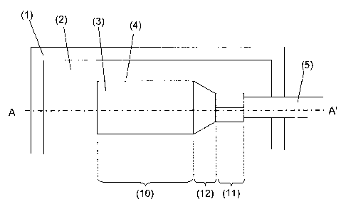
Fig.1 and Fig. 2 depict in each case a detail of a pane according to the
invention in the
region of the electrical connection element 3. The pane comprises a substrate
1, which is a
3-mm-thick thermally prestressed single pane safety glass made of soda lime
glass. The
substrate 1 has a width of 150 cm and a height of 80 cm. An electrically
conductive structure
2 in the form of a heating conductor structure is printed on the substrate 1.
The electrically
conductive structure 2 contains silver particles and glass frits. In the edge
region of the
pane, the electrically conductive structure 2 is widened to a width of 10 mm
and forms a
contact surface for an electrical connection element 3. The connection element
3 serves for
the electrical contacting of the electrically conductive structure 2 with an
internal power
supply via a connection cable 5. The connection cable 5 includes an
electrically conductive
core that is implemented as a conventional stranded wire conductor made of
copper. The
connection cable 5 further includes a polymer insulating sheathing (not shown)
that is
removed in the end region to the length of 4.5 mm to enable the electrical
contacting of the
electrically conductive core of the connection cable 5 with the connection
element 3. A
covering screenprint (not shown) is also situated in the edge region of the
substrate 1.
CA 02884779 2015-03-11
13
The electrical connection element 3 is made of steel of the material number
1.4509 in
accordance with EN 10 088-2 (ThyssenKrupp Nirosta 4509) with a coefficient of
thermal
expansion of 10.5 x 10⁻⁶/0C in the temperature range from 20 C to 300 C. The
material
thickness of the connection element 3 is, for example, 0.4 mm. The connection
element has
a region 11 with a length of, for example, 4 mm, which is crimped around the
end region of
the connection cable 5. For this, the side edges of the crimped region 11 are
bent around
the connection cable 5 and squeezed therewith. The crimp is disposed such that
the region
of the substrate 1 bent around points away from the substrate 1. By this
means, an
advantageously small angle can be realized between the crimped region 11 and
the
substrate 1. However, in principle, the reversed arrangement of the crimp is
also possible.
The connection element 3 further has a substantially rectangular, flat solder
region 10, which
is connected to the crimped region 11 via a transition region 12. The solder
region 10 has,
for example, a length of 4 mm and a width of 2.5 mm. The transition region 12
has, for
example, a length of 1 mm. The solder region 10 is disposed on the side of the
crimped
region 11 that faces the extension direction of the connection cable 5. The
angle between
the solder region 10 and the crimped region 11 is, for example, 160 . The
transition region
12 is implemented flat, but can, for example, alternatively also be
implemented curved
and/or bent.
The surface of the solder region 10 facing the substrate 1 forms a contact
surface 8 between
the electrical connection element 3 and the electrically conductive structure
2. Solder
material 4, which effects a durable electrical and mechanical connection
between the
electrical connection element 3 and the electrically conductive structure 2,
is applied in the
region of the contact surface 8. The solder material 4 contains 57 wt.-%
bismuth, 40 wt.-%
tin, and 3 wt.-% silver. The solder material 4 has a thickness of 250 pm. The
solder region
is connected to the electrically conductive structure 2 via the contact
surface 8 over its
entire area.
Fig. 3 depicts a cross-section through an alternative embodiment of the pane
according to
the invention with the connection element 3. The contact surface 8 of the
connection
element 3 is provided with a silver-containing wetting layer 6, for example,
with a thickness
of roughly 5 m. This improves the adhesion of the connection element 3. In
another
embodiment, an adhesion-promoting layer, made, for example, of nickel and/or
copper can
be situated between the connection element 3 and the wetting layer 6.
CA 02884779 2015-03-11
14
Fig. 4 depicts a cross-section through an alternative embodiment of the pane
according to
the invention with the connection element 3. Spacers 7 are disposed on the
contact surface
8 of the connection element 3. For example, four spacers 7, of which two
spacers 7 can be
discerned in the section depicted, can be disposed on the contact surface 8.
The spacers 7
are stamped into the solder region 10 of the connection element 3 and thus
implemented in
one piece with the connection element 3. The spacers 7 are shaped as spherical
segments
and have a height of 2.5 x 10⁻⁴ m and a width of 5 x 10⁻⁴ m. By means of the
spacers 7, the
formation of a uniform layer of the solder material 4 is promoted. This is
particularly
advantageous with regard to the adhesion of the connection element 3.
Fig. 5 depicts a cross-section through an alternative embodiment of the pane
according to
the invention with the connection element 3. A contact bump 9 is disposed on
the surface of
the soldering region 10 of the connection element 3 facing away from the
substrate 1 and
opposite the contact surface 8. The contact bump 9 is stamped into the solder
region 10 of
the connection element 3 and thus implemented in one piece with the connection
element 3.
The contact bump 9 is shaped as a spherical segment and has a height of 2.5 x
10-4 m and
a width of 5 x 10⁻⁴ m. The contact bump 9 serves for the contacting of the
connection
element 3 with the soldering tool during the soldering process. By means of
the contact
bump 9, a reproducible and defined heat distribution is ensured independent of
the exact
positioning of the soldering tool.
Fig. 6 depicts a cross-section through an alternative embodiment of the pane
according to
the invention with the connection element 3. The electrical connection element
3 includes,
on the contact surface 8 facing the solder material 4, a recess with a depth
of 250 pm, which
is stamped into the solder region 10 and which forms a solder depot for the
solder material
4. Outflow of the solder material 4 from the intermediate space can be
completely prevented.
By this means, the thermal stresses in the pane are further reduced.
Fig. 7 depicts a cross-section through an alternative embodiment of the pane
according to
the invention with the connection element 3. The connection element 3 has, in
addition to
the crimped region 11, the transition region 12, and the solder region 10, a
further region 13,
adjacent the solder region 10. The further region 13 and the transition region
12 with the
crimped region 11 are connected to opposing edges of the solder region 10.
Fig. 8 depicts in detail a method according to the invention for production of
a pane with an
electrical connection element 3.
CA 02884779 2015-03-11
Test specimens were produced with the substrate 1 (thickness 3 mm, width 150
cm, and
height 80 cm), the electrically conductive structure 2 in the form of a
heating conductor
structure, the electrical connection element 3 according to Fig. 1, and the
solder material 4.
The connection element 3 was made of steel of the material number 1.4509 in
accordance
with EN 10 088-2, which has a coefficient of thermal expansion of 10.0 x 10-61
C in the
temperature range from 20 C to 200 C and a coefficient of thermal expansion of
10.5 x 10-61 C in the temperature range from 20 C to 300 C. The substrate 1
was made of
soda lime glass with a coefficient of thermal expansion of 8.30 x 10⁻⁶/ C in
the temperature
range from 20 C to 300 C. The solder material 4 contained Sn40Bi57Ag3 and had
a layer
thickness of 250 gm. The connection element 3 was soldered onto the
electrically
conductive structure 2 at a temperature of 200 C and a processing time of 2
seconds. No
critical mechanical stresses were observed in the pane. The connection of the
pane to the
electrical connection element 3 via the electrically conductive structure 2
was durably stable.
With all specimens, it was possible to observe, with a temperature difference
from +80 C to
-30 C, that no substrate 1 broke or showed damage. It was possible to
demonstrate that,
shortly after soldering, the panes with the soldered connection element 3 were
stable
against a sudden temperature drop.
In comparative examples with connection elements that had the same shape and
were
made of copper or brass, clearly greater mechanical stresses occurred and with
a sudden
temperature difference from +80 C to -30 C, it was observed that the pane
had major
damage shortly after soldering. It was demonstrated that panes according to
the invention
with glass substrates 1 and electrical connection elements 3 according to the
invention had
better stability against sudden temperature differences. This result was
unexpected and
surprising for the person skilled in the art.
CA 02884779 2015-03-11
16
List of Reference Characters
(1) substrate
(2) electrically conductive structure
(3) electrical connection element
(4) solder material
(5) connection cable
(6) wetting layer
(7) spacer
(8) contact surface of the connection element 3 with the electrically
conductive
structure 2
(9) contact bump
(10) solder region of the connection element 3
(11) crimped region of the connection element 3
(12) transition region between the crimped region 11 and the solder region 10
(13) another region of the connection element 3
A-A' section line