Note: Descriptions are shown in the official language in which they were submitted.
CA 02884886 2015-03-12
WO 2014/081543 PCT/US2013/067648
DUAL LINEAR AND CIRCULARLY POLARIZED PATCH RADIATOR
FIELD
[0001] The concepts, systems, circuits, devices and techniques described
herein
relate generally to radio frequency (RF) circuits and more particularly to RF
antennas.
BACKGROUND
[00021 As is known in the art, a so-called patch antenna element (also
referred
to as "a patch element" or more simply "a patch") is a basic building block a
number of different types of phased array antenna including so-called panel
phased arrays (or panel arrays) such as the types described in U.S. Patents
7,348,932; 7,671,696; and 8,279,131, all of which are assigned to the assignee
of
the present application. The patch element is integrated within a panel array
to
allow for the use of low cost printed wiring board (PWB) processes in the
manufacture of the panel array.
[9003] Referring now to Fig. 1, a conventional patch element 2 and feed
circuit 3
are coupled to provide a conventional patch radiator 4. The patch element is
provided from a conductor disposed on a first surface of a substrate. A slot 5
is
etched or otherwise provided in the conductor. The feed circuit 4 is provided
fivin
a single feed line 7 disposed on a second opposite surface of the substrate. A
first end of the feed line corresponds to an antenna feed port 4A and a second
end of the feed line 4B is coupled to a ground plane through a conductive via.
An
open ended stub 8 is coupled to feed line 7 as is generally known. Patch
radiator
4 is responsive to radio frequency (RF) signals having a single linear
polarization.
[00041 In operation, an RF signal provided to the antenna feed port 4A is
coupled via feed line 7 to the open ended stub 8 thereby illuminating slot 5,
which
in turn excites the patch 2. Similarly, signals provided to patch conductor 2
illuminate the slot 5 and are coupled via the open ended stub 8 and feed line
7 to
the feed line antenna feed port 4k Thus, the patch radiator 4 operates for
both
transmitting and receiving RF signals.
CA 02884886 2015-03-12
WO 2014/081543 PCMS2013/067648
[0005] As mentioned above, however, patch radiator 4 can be used only for a
single polarization. This is due to the topology of the patch element 2 and
feed
circuit 3. To support dual and/or circular polarization, a more complicated
geometry is required as illustrated in F. 2.
[00061 Referring now to Fig. 2, to support dual and/or circular polarization
in one
type of conventional patch radiator, a feed circuit comprising four feed lines
(and
thus four antenna feed ports) is required. Essentially, the single stub
described
above in conjunction with Fig. I is split into two open ended stubs (e.g. one
to
excite vertically polarized RF signals and one to excite horizontally
polarized RF
signals). To support dual linear polarization, both stubs (for each
excitation) are
driven in phase. This is conventionally accomplished via a microwave power
divider circuit (not shown in Fig. 2). Simple geometry dictates the need four
four
feeds. The single polarization example (Fig. 1) places the open ended stub
along
the center line.. However, it is not possible to place two perpendicular open
ended
stubs, each aligned to the center line without them being shorted to each
other.
Therefore two open ended stubs are required for each polarization
[00071 Circular polarization may be obtained by introducing a ninety (90)
degree
phase shift between signals provided to (or received from) the horizontal and
vertical stubs. Such a 90 degree phase shift can be accomplished using a
ninety
(90) degree hybrid coupler (not shown in Fig. 2) or by controlling the phases
independently in control circuitry (not shown in Fig,2). Therefore, to extend
the
operation of a patch radiator from a single linear polarization to operation
with dual
linear or circular polarization requires the addition of much circuitry (e.g.
a power
divider or hybrid coupler) to the feed circuit.
[0008] In a phased array antenna in which space in limited, it is difficult to
fit
such additional circuitry (e.g. additional power divider or hybrid coupler
circuitry)
within a so-called unit cell which includes an antenna element (e.g. one or
more
patch elements) and the associated feed circuitry. it would, therefore, be
desirable to provide a patch radiator operable for use with dual linear or
circular
CA 02884886 2015-03-12
WO 2014/081543 PCT/US2013/067648
polarization RF signals and which is compact enough for use in phased array
antennas.
SUMMARY
[00091 In accordance with the concepts, systems and circuits described herein,
a
patch radiator suitable for operation with dual linear or circularly polarized
radio
frequency (RF) signals includes a patch antenna element and a feed circuit.
The
feed circuit includes a feed line terminating in a stub region having an open
circuit
impedance characteristic and a tuning stub disposed a selected distance from
the
open circuit stub region of the feed line with the tuning stub selected to
provide an
impedance characteristic which establishes resonance with the feed line at a
desired frequency.
[0010] With this particular arrangement, a patch radiator capable of dual
linear or
circular polarization operation and suitable for use in a unit cell of a
phased array
antenna is provided. By utilizing a tuning stub to establish resonance with a
single
feed line, a single antenna feed port can be used for operation of the patch
radiator
at dual linear or circular polarizations without the use of external circuitry
such as
power divider circuits, hybrid circuits or any other type of power splitting
circuitry (MI
such circuitry collectively referred to herein as "power splifter circuits").
The tuning
stub establishes an appropriate impedance to set up a standing wave between
two
open ended stubs coupled to the patch antenna element. This requires tuning
the
open to set up the resonance between the feed and the tuned stubs. To a zeroth
order approximation, the length of the opens should be 1/.'1, wavelength to
get the
desired resonance. However, due to the complex coupling of the design, the
correct length is obtained through iterative numerical simulations,
[owl Although the above-described single feed line4uning stub approach works
over a limited bandwidth (e,g, a 10% bandwidth), since the patch antenna
element
itself only wanks well over a limited bandwidth, this is not a major
limitation to
operation of a patch radiator. Moreover, by eliminating the need for power
splitter
circuits to achieve dual linear or circular polarization, the radiation
efficiency of this
approach is higher than that of conventional approaches as the losses from
such
3
CA 02884886 2015-03-12
WO 2014/081543 PCT/US2013/067648
power spfitter circuits are eliminated.
[0012] Furthermore, the tuning stub enables the patch radiator to operate with
dual linear or circular polarization while using only two feed lines whereas
prior art
techniques require four feed lines. By eliminating two feed line and two power
splitter circuits, the patch radiator as described herein (Le. the combination
of the
antenna element and associated antenna element feed circuit) is made more
compact compared with conventional patch radiators.
[0013] The compact patch antenna element described herein is thus able to fit
within an area defined by a unit mil of a phased array antenna In one
embodiment, the compact patch radiator is able to fit an RF circuit card
assembly
(RF-CCA) of a phased array operating at frequencies higher than X-Band. The
dual polarization phased array patch radiator has a footprint which is smaller
than
conventional dual polarization patch radiators because it eliminates the need
for
power splitters. The relatively small footprint allows for RF-CCA operation at
higher
frequency (e.g. Ku-Band) as the unit cell area scales inversely as the square
of the
frequency. Furthermore, the dual polarization phased array patch radiator is
compatible with existing RF-CCA fabrication processes and scales with
frequency.
[0014] The patch element includes a single feed per polarization and is
capable of
operation in two polarizations. When the patch element operates in one
polarization, the opposite feed is terminated. With the two linear
polarization feed
circuits, circular polarization is created by correct phasing of the two
linear inputs.
The 90 degree phasing can be obtained by either an analog circuit or through
digital
control. The analog implementation required including on other layers of the
PWB a
90 degree hybrid circuit, The digital implementation requires that the
attenuatoriphase shifter control chip have dual outputs that have differential
phase
control For circular polarization the difference would be either +1- 90
degrees. This
functionality would be required for both transmit and receive.
4
CA 02884886 2015-03-12
WO 2014/081543 PCT/US2013/067648
[0015] in accordance with the concepts, systems and circuits described herein,
an
antenna comprises a patch element having a pair of excitatkm circuits with one
side
of each excitation pair grounded at an appropriately tuned position and the
other
side used to transmit or receive signals from the patch element, An actual
design
will require iterative numerical simulations to determine the correct length
for a
specific frequency and PWS design,
[0016] With this particular arrangement, a patch radiator suitable for
operation
with dual linear or circular polarization while eliminating need for a two
sided feed
for each excitation is provided. One side of each excitation pair is grounded
at an
appropriate position and the other side is used as to transmit or receive from
the
patch element. This eliminates the need for power divider circuitry needed in
conventional dual polarization patch radiators. The presence of a grounded
stubs
in the excitation circuits acts as a tuned ''reflector and keeps the
polarization
purely linear and efficiently couples the electric fields between the stub,
slot and
patch. Without the grounded stub, the off center excitation creates a
radiation
pattern that is not linear. Without two orthogonal linear excitations, it is
not
possible to generate circular polarization with low axial ratio.
[0017] The efficiency of a conventional dual stub approach is degraded by the
cross talk between the two stubs, In transmit mode, the microwave radiation
launched from one stub is absorbed at the other and then travels back to the
source. This is energy that is not launched through the patch. Typical
efficiencies
of such conventional designs at 10 GHz are about 60%.
[0018] The shorted stub approach described herein, on the other hand, resuits
in
efficiencies which can be as high as 80%,
[0019] In accordance with a still further aspect of the concepts, systems and
circuits described herein, a circularly polarized patch radiator includes a
patch
antenna element and a pair of excitation circuits with one side of each
excitation
pair grounded at an appropriate position and the other side used to transmit
or
:3
CA 02884886 2015-03-12
WO 2014/081543 PCT/US2013/067648
receive from the patch antenna element,
[0020] In one embodiment, the patch antenna element is provided from an
antenna conductor disposed on a substrate with first and second slots disposed
in a
first direction in the antenna conductor and third and fourth slots disposed
in a
second, orthogonal direction in the antenna conductor,
[0021] In one embodiment, each excitation circuit includes a feed line
terminated
in an open circuit impedance and a tuning circuit disposed a selected distance
from
the feed line with the tuning circuit selected to provide an impedance
characteristic
which establishes resonance with the feed line at a desired frequency.
[0022] In one embodiment, the feed lines of the respective excitation circuits
are
coupled to adjacent sides of the antenna conductor.
[0023] in one embodiment, the tuning circuit is provided as a tuning stub
having a
shape selected to provide an impedance characteristic which establishes
resonance with the feed line at a desired frequency,
[0024] In accordance with a still further aspect of the concepts, systems and
circuits described herein, a phased array antenna includes a plurality of
patch
radiatiors, each of the patch radiators including a patch antenna element and
a
pair of excitation circuits with one side of each excitation pair being
grounded at
an appropriate position and the other side used to transmit and/or receive
from the
patch antenna element which enables the patch radiators to be responsive to RE
signals having circular polarization.
100251 In one embodiment, the excitation circuits comprise a feed circuit
which
includes a feed line terminating in a stub region having an open circuit
impedance
characteristic and a tuning circuit disposed to provide an impedance
characteristic
which establishes resonance with the feed line at a desired frequency.
6
CA 02884886 2015-03-12
WO 2014/081543 PerfUS2013/067648
[0026] In one embodiment, the tuning circuit is provided as a tuning stub
having a
shape selected to provide an impedance characteristic which establishes
resonance with said feed line at a desired frequency.
[0027] in accordance with a still further aspect of the concepts, systems and
circuits described herein, a patch radiator suitable for operation with
circular or
dual linear polarizations includes a patch antenna element and a pair of
excitation
circuits The excitation circuits include a feed line and a turning circuit
configured
such that a single feed line enables independent operation of each
polarization.
This allows for the operation of the patch and therefore array as either
linear,
slant, elliptical, or circular polarization.
[0028] It should be appreciated that this Summary is provided to introduce a
selection of concepts in a simplified form that are further described below in
the
Detailed Description.
BRIEF DESCRIPTION OF THE DRAWINGS
[0029] The foregoing and other objects, features and advantages of the
concepts, systems, circuits and techniques described herein will be apparent
from
the following description of particular exemplary embodiments as illustrated
in the
accompanying drawings in which like reference characters refer to like
elements
throughout the different views, The drawings are not necessarily to scale,
emphasis instead being placed upon illustrating the concepts, systems,
circuits
and techniques,
[0030] Fig. I is an isometric view of a conventional patch radiator having a
patch
element and a single feed line and suitable for transmitting or receiving
radio
frequency (RF) signals having a single linear polarization;
[0031] Fig, 2 is an isometric view of a conventional patch radiator having a
patch
element and four feed lines and suitable for transmitting or receiving RF
signals
having dual or circular polarization;
'7
CA 02884886 2015-03-12
WO 2014/081543 PCT/US2013/067648
[00321 Fig, 3 is an isometric view of a patch radiator suitable for
transmitting
and/or receiving RF signals having dual or circular polarization;
[00331 Fig. 3A is an exploded isometric view of a patch radiator suitable for
transmitting and/or receiving RF signals having dual or circular polarization
[0034] Figs. 4A, 4B, 4C are a series of top views of various types of patch
antenna element topologies suitable for use as a patch radiator of the type
described above in conjunction with Fig. 3;
[0035] Fig, 5 is a plan view of an panel array antenna utilizing a patch
radiator
which may be the same as or similar to the patch radiator of Fig. 3; and
[0036] F. 6 is a perspective view of a panel sub-an-ay of the type used in
panel
array antenna shown in FIG. 5.
DETAILED DESCRIPTION
100371 Before describing an exemplary embodiment of a patch radiator
responsive to dual linear or circular polarization, it should be appreciated
that using
the concepts described herein one can eliminate the two sided feed for each
excitation which is conventionally needed for antenna operation with dual
linear or
circular polarization as shown in the exemplary embodiment of Fig. 2. Thus,
the
patch radiator described herein below utilizes an excitation circuit having
only a
single feed for each polarization. As will become apparent from the
description
herein below, one side of each excitation pair is grounded at an appropriate
position and the other side is used as to transmit or receive from a patch,
[0038] This technique eliminates the need for power splitter circuitry
conventionally required for antenna operation with dual linear or circular
polarization. The presence of the grounded stub acts as a tuned "reflectors'
and
keeps the polarization purely linear and efficiently couples the electric
fields
between the stub, slot and patch. Without the grounded stub, the off center
excitation creates a radiation pattern that is not linear and without two
orthogonal
8
CA 02884886 2015-03-12
WO 2014/081543 PerfUS2013/067648
linear excitations, it is not possible to generate circular polarization
having a low
axial ratio.
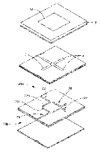
[0039,1 Retening now to Figs, 3 and 3A in which like elements are provided
having
like reference designations, a patch radiator 10 includes a patch element 12
and a
feed circuit 14. Patch element 12 is provided from a conductor 16 disposed
over a
first surface of a substrate 18.
[0040] A pair of excitation circuits 20a, 20b are comprised of respective feed
lines
22, 24 each of which include respective ones of stub regions 22a, 24a having
open
circuit impedance characteristics, Excitation circuits 20a, 20b also include
respective ones of tuning circuits 26, 28. Tuning circuits 26, 28 are disposed
to
provide an impedance characteristic which establishes resonance with
respective
feed ones 22, 24 at a desired frequency.
[0041] in the exemplary embodiment of Figs. 3, 3A tuning circuits 26, 28 are
implemented as tuning stubs having a first end terminated in an open circuit
impedance characteristic and having a second end terminated in a short circuit
impedance characteristic. in one embodiment, the turning stubs are implemented
as L-shaped conductors disposed on a second opposite surface of the substrate
in
which the patch element conductor s are disposed.
[0042] Thus, as is apparent from Figs. 3, 3A, one side of each excitation pair
is
terminated at a position which results in an impedance characteristic which
establishes resonance with a respective feed line a desired frequency. The
presence of the stub acts as a tuned reflector and keeps the polarization
purely
linear and efficiently couples the electric fields between the stub, slot and
patch
element conductor.
[0043] Before describing the patch radiator described above in conjunction
with
Figs. 3 and 3A as included in a panel array antenna, some introductory
concepts
and terminology are explained. A "panel array (or more simply "panel) refers
to a
multilayer printed wiring board (PWB) which includes an array of antenna
9
CA 02884886 2015-03-12
WO 2014/081543 PCT/US2013/067648
elements (or more simply "radiating elements" or "radiators"). A panel array
often
also includes RF, logic and DC distribution circuits in one highly integrated
MB.
A panel is also sometimes referred to herein as a the array (or more simply, a
"tile").
[0044] An array antenna may be provided from a single panel (or tile) or from
a
plurality of panels. In the case where an array antenna is provided from a
plurality
of panels, a single one of the plurality of panels is sometimes referred to
herein as
a "panel sub-arrar (or a "tile sub-array').
[0046] Reference is sometimes made herein to a panel array antenna having a
particular number of panels. It should of course, be appreciated that an array
antenna may be comprised of any number of panels and that one of ordinary
skill
in the art will appreciate how to select the particular number of panels to
use in
any particular application.
[0046] It should also be noted that reference is sometimes made herein to a
panel or an array antenna having a particular array shape and/or physical size
and lattice spacing or a particular number of antenna elements. One of
ordinary
skill in the art will appreciate that the techniques described herein are
applicable
to various sizes, lattice spacing and shapes of panels and/or array antennas
and
that any number of antenna elements may be used.
[0047] Similarly, reference is sometimes made herein to panel or the sub-
arrays
having a particular geometric shape (e.g, square, rectangular, round) and/or
size
a particular number of antenna elements) or a particular lattice type or
spacing of antenna elements. One of ordinary skill in the art will appreciate
that
the patch radiator and techniques related thereto as described herein are
applicable to various sizes and shapes of array antennas as well as to various
sizes and shapes of panels (or tiles) and/or panel sub-arrays (or tile sub-
arrays).
[00441 Those of ordinary skill in the art, after reading the description
provided
herein, will appreciate that the size of one or more antenna elements may be
CA 02884886 2015-03-12
WO 2014/081543 PCT/US2013/067648
selected for operation at any frequency in the RE frequency range (e.g. any
frequency in the range of about 400 MHz GHz to about 100 GHz).
[0049] It should also be appreciated that the antenna elements in each panel
or
the sub-array can be provided having any one of a plurality of different
antenna
element lattice arrangements including periodic lattice arrangements (or
configurations) such as rectangular, square, triangular (e.g. equilateral or
isosceles triangular), and spiral configurations as well as non-periodic or
arbitrary
lattice arrangements.
[0050] Applications of at least some embodiments of the patch radiator panel
array (alkia tile array) architectures described herein include, but are not
limited
to, radar, electronic warfare (EW) and communication systems for a wide
variety
of applications including ship based, ground based, airborne, missile and
satellite
applications.
[00511 As will also be explained further herein, at least some embodiments of
the invention are applicable, but not limited to, military, airborne, ship
borne,
ground based, communications, unmanned aerial vehicles (UAV) and/or
commercial wireless applications.
[0052] It should be appreciated that in both Figs, 5 and 6 the successive rows
are staggered. There is also the case where the successive rows are aligned.
Also, in the general case (rather than the specific exemplary embodiment shown
in Figs. 5 and 6) the pitch in the x any directions may not be the same.
[0053] Turning now to Fig, 5, an array antenna 40 is comprised of a plurality
of
tile sub-arrays 42a ¨ 42x, It should be appreciated that in this exemplary
embodiment, x total tile sub-arrays 42 comprise the entire array antenna 40.
In
one embodiment, the total number of tile sub-arrays is sixteen tile sub-arrays
(i.e.
x = 16). The particular number of tile sub-arrays 42 used to provide a
complete
array antenna can be selected in accordance with a variety of factors
including,
but not limited to, the frequency of operation, array gain, the space
available for
CA 02884886 2015-03-12
WO 2014/081543 PCT/US2013/067648
the array antenna and the particular application for which the array antenna
40 is
intended to be used. Those of ordinary skill in the art will appreciate how to
select
the number of the sub-arrays 42 to use in providing a complete array antenna,
[0054] As illustrated in tiles 42b and 42i, in the exemplary embodiment of
Fig, 5,
each tile sub-array 42a -42x comprises eight rows 43a - 43h of antenna
elements
45 with each row containing eight antenna elements 45 (or more simply,
"elements 45). Each of the tile sub-arrays 42a - 42x is thus said to be an
eight by
eight (or 8x8) tile sub-array. It should be noted that each antenna element 45
is
shown in phantom in Fig. 5 since the elements 45 are not directly visible on
the
exposed surface (or front face) of the array antenna 40. Each element 45 may
be
the same as or similar to patch radiator 10 described above in conjunction
with
Figs, 3 and 3A. In this particular exemplary embodiment, each tile sub-array
42a -
42x comprises sixty-four (64) antenna elements. In the case where the array 40
is
comprised of sixteen (16) such tiles, the array 40 comprises a total of one-
thousand and twenty-four (1,024) antenna elements 45.
[0055] In another embodiment, each of the tile sub-arrays 42a-42x comprise 16
elements, Thus, in the case where the array 40 is comprised of sixteen (16)
such
tiles and each tiles comprises sixteen (16) elements 45, the array 40
comprises a
total of two-hundred and fifty-six (256) antenna elements 45.
[0056] In still another exemplary embodiment, each of the tile sub-arrays 42a -
42x comprises one-thousand and twenty-four (1024) elements 45. Thus, in the
case where the array 14 is comprised of sixteen (16) such tiles, the array 40
comprises a total of sixteen thousand three-hundred and eighty-four (16,384)
antenna elements 45,
[0057] In view of the above exemplary embodiments, it should thus be
appreciated that each of the tile sub-arrays can include any desired number of
elements. The particular number of elements to include in each of tile sub-
arrays
42a-42x can be selected in accordance with a variety of factors including but
not
limited to the desired frequency of operation, array gain, the space available
for
12
CA 02884886 2015-03-12
WO 2014/081543 PCT/US2013/067648
the antenna and the particular application for which the array antenna 40 is
intended to be used and the size of each sub-array 42. For any given
application,
those of ordinary skill in the art will appreciate how to select an
appropriate
number of radiating elements to include in each tile sub-array. The total
number
of antenna elements 45 included in a panel antenna array such as antenna array
40 depends upon the number of subarrays included in the antenna array and as
well as the number of antenna elements included in each subarray.
[00581 As will become apparent from the description hereinbelows each sub.
array is electrically autonomous (excepting of course any mutual coupling
which
occurs between elements 45 within a the and on different fifes). Thus, the RF
feed
circuitry which couples RF energy to and from each radiator on a tile is
incorporated entirely- within that tile (Le, ail of the RF feed and
beamfomling
circuitry which couples RF signals to and from elements 46 in tile 42b are
contained within tile 42b). Each tile includes one or more RF connectors and
the
RF signals are provided to the tile through the RF connector(s) provided on
each
tile sub-array.
P059] Also, signal paths for logic signals and signal paths for power signals
which couple signals to and from transmit/receive (TIR) circuits are contained
within the tile in which the TIR circuits exist.
[0060] The RF beam for the entire array 40 is formed by an external beamformer
(Le. external to each of the subarrays 42) that combines the RF outputs from
each
of the tile sub-arrays 42a-42x. As is known to those of ordinary skill in the
art, the
beamformer may be conventionally implemented as a printed wiring board
stripline circuit that combines N sub-arrays into one RF signal port (and
hence the
beamformer may be referred to as a 1:N beamformer),
(00611 The sub-arrays may be mechanically fastened or otherwise secured to a
mounting structure using conventional techniques such that the array lattice
pattern is continuous across each tile which comprises the array antenna. In
one
embodiment, the mounting structure may be provided as a "picture frame" to
13
CA 02884886 2015-03-12
WO 2014/081543 PCT/US2013/067648
which the tile-subarrays are secured using fasteners (such as #10-32 size
screws,
for example). The tolerance between inteilocking sections of the tile is
preferably
in the range of about +/-.005 in for 10 Gl-lz operation although larger
tolerances
may also be acceptable and smaller tolerances may be required based upon a
variety of factors including but not limited to the frequency of operation.
Preferably, the arrays 42a ¨ 42x are mechanically mounted such that the array
lattice pattern (which is shown as a triangular lattice pattern in exemplary
embodiment of Fig, 4) appears electrically continuous across the entire
surface
40a (or 'face") of the panel array 40.
100621 Advantageously, the sub-array embodiments described herein can be
manufactured using standard printed wiring board (RNB) manufacturing
processes to produce highly integrated, passive RF circuits, using commercial,
off-the-shelf (COTS) microwave materials, and highly integrated, active
monolithic
microwave integrated circuits (MIVIIC's). This results in reduced
manufacturing
costs, Array antenna manufacturing costs can also be reduced since the tile
sub-
arrays can be provided from relatively large panels or sheets of PWBs using
conventional PWB manufacturing techniques,
[0063] In one exemplary embodiment, a panel array having dimensions of 0,5
meter x 0.5 meter and comprising 1024 dual circular polarized antenna elements
was manufactured on one sheet (or one multilayer PWB). The techniques
described herein allow standard printed wiring board processes to be used to
fabricate panels having dimensions up to and including imxim with up to 4096
antenna elements from one sheet of multi-layer printed wiring boards (PWBs).
Fabrication of array antennas utilizing large panels reduces cost by
integrating
many antenna elements with the associated RF feed and beamforming circuity
since a "batch processing" approach can be used throughout the manufacturing
process including fabrication of TiR channels in the array. Batch processing
refers to the use of large volume fabrication and/or assembly of materials and
components using automated equipment. The ability to use a batch processing
approach for fabrication of a particular antenna design is desirable since it
generally results in relatively low fabrication costs. Use of the tile
architecture
14
CA 02884886 2015-03-12
WO 2014/081543 PCT/US2013/067648
results in an array antenna having a reduced profile and weight compared with
prior art arrays of the same size (i.e. having substantially the same physical
dimensions).
[0064] Referring now to Fig. 6 in which like elements of F. 4 are provided
having like reference designations, and taking the sub-array 42b as
representative
of tile sub-arrays 42a and 42o-42x, the the sub-array 42b includes a radiator
subassembly 52 which, in this exemplary embodiment, is provided as a so-called
"dual circular polarized patch radiator.
[0066] The radiator subassembly 62 is provided having a first surface 62a
'which
can act as a radome and having a second opposing surface 52b. The radiator
assembly 22 is comprised of a plurality of microwave circuit boards (also
referred
to as PWB,$) (not visible in Fig, 5). Radiator elements 45 are shown in
phantom in
Figs. 6 and 6 since they are disposed below the surface 52a and thus are not
directly visible in the view of Fig. 5.
[0066] The radiator subassembly 52 may be disposed over a plurality of other
PWBs.
mon While particular embodiments of the present invention have been shown
and described, it will be apparent to those skilled in the art that various
changes
and modifications in form and details may be made therein without departing
from
the spirit and scope of the concepts as defined by the following claims. For
example, although the description provided herein above describes the concepts
in the context of an array antenna having a substantially square or
rectangular
shape and comprised of a plurality of tile sub-arrays having a substantially
square
or rectangular-shape, those of ordinary skill in the art will appreciate that
the
concepts equally apply to other sizes and shapes of array antennas and panels
(or tile sub-arrays) having a variety of different sizes and shapes. Also, the
panels
(or tiles) may be arranged in a variety of different lattice arrangements
including,
but not limited to, periodic laftice arrangements or configurations (e.g.
rectangular,
circular, equilateral or isosceles triangular and spiral configurations) as
well as
CA 02884886 2015-03-12
WO 2014/081543 PCT/US2013/067648
non-penodic or other geometric arrangement: including arbitrarily shaped array
geometries. Accordingly, the appended claims encompass within their scope all
such changes and modifications.
16