Note: Descriptions are shown in the official language in which they were submitted.
CA 02886246 2015-03-25
WO 2014/052773
PCT/US2013/062208
DROOP COMPENSATION USING CURRENT FEEDBACK
[0001] The
present application claims priority to U.S. Provisional Application Serial
No. 61/707,478, filed September 28, 2012, the entirety of which is hereby
incorporated
herein by reference.
FIELD
[0002] The
present invention is generally related to power sources, and more
particularly to controllers associated therewith.
BACKGROUND
[0003] It is
often advantageous to couple different power sources together to supply a
greater quantity of power than achievable by any individual source. For
example,
electrochemical cells are often coupled together to form electrochemical cell
systems
(i.e., batteries). In some electrochemical cell systems, it may be
advantageous to control
each electrochemical cell therein, or subsets of the electrochemical cells
therein, so as to
increase overall system efficiency in supplying power to a load. For example,
where one
or more electrochemical cells (e.g., grouped into modules) in the
electrochemical cell
system fail or experience a performance drop relative to the other
electrochemical cells or
modules, it may be desirable to attempt to equalize currents between different
cells, while
sharing power between the modules. In particular, generally equal module
lifespan across
the system may be based more on the current draw associated with each module
than on
the total energy or power supplied by the module. Such a configuration may
facilitate a
uniform replacement schedule for modules in the system by generally equalizing
the
lifespans of each of the modules of the system.
[0004]
Conventionally, to share currents across electrochemical cells, slave cells or
modules are tied to a master cell or module, so that the master cell or module
establishes
the current draw for the system. Where the master cell or module fails or
experiences
other performance degradation, however, the entire system's performance may
correspondingly degrade. Among other disadvantages, this conventional method
fails to
maintain the independence of modules.
1
CA 02886246 2015-03-25
WO 2014/052773
PCT/US2013/062208
[0005]
Accordingly, the disclosure of the present application endeavors to
accomplish these and other results.
SUMMARY
[0006]
According to an embodiment, a system includes a boost converter configured
to amplify input voltage received from one or more power sources into output
voltage.
The system also includes a current sensor configured to sense a current of the
input
voltage. Current can be measured by a magnetic method (i.e. induction) or
purely
resistive method (i.e. precise resistor) or a combination of these methods.
The system
further includes a controller configured to adjust an amplification of the
boost converter
in response to the current sensed by the current sensor.
[0007]
According to another embodiment, a system includes a plurality of power
source modules. Each power source module includes a boost converter configured
to
amplify input voltage received from one or more power sources into output
voltage. Each
power source module also includes a current sensor configured to sense a
current of the
input voltage for example, by induction. Each power source module further
includes a
controller configured to adjust an amplification of the boost converter in
response to the
current sensed by the current sensor. The plurality of power source modules
are coupled
to a common load through the output voltage. The plurality of power source
modules
adjust the amplifications of their boost converters towards equalization of
their output
voltages and their currents in response to sensed currents of the input
voltages changing
through demand of the common load.
[0008]
According to another embodiment, a method of equalizing current across a
plurality of power sources coupled to a common load includes, for each of the
power
sources, amplifying, using a boost converter, input voltage received from one
or more
power sources into output voltage. For each of the power sources, the method
also
includes sensing, using a current sensor, a current of the input voltage by
induction. For
each of the power sources, the method further includes adjusting an amount of
said
amplifying in response to the current sensed by the current sensor. By
adjusting the
amount of said amplifying, the plurality of power sources approach a stable
equilibrium
of output voltages and currents.
2
CA 02886246 2015-03-25
WO 2014/052773
PCT/US2013/062208
[0009] Other
aspects of the present invention will become apparent from the
following detailed description, the accompanying drawings, and the appended
claims.
BRIEF DESCRIPTION OF THE DRAWINGS
[0010]
Embodiments of the invention will now be described, by way of example
only, with reference to the accompanying schematic drawings in which
corresponding
reference symbols indicate corresponding parts, and in which:
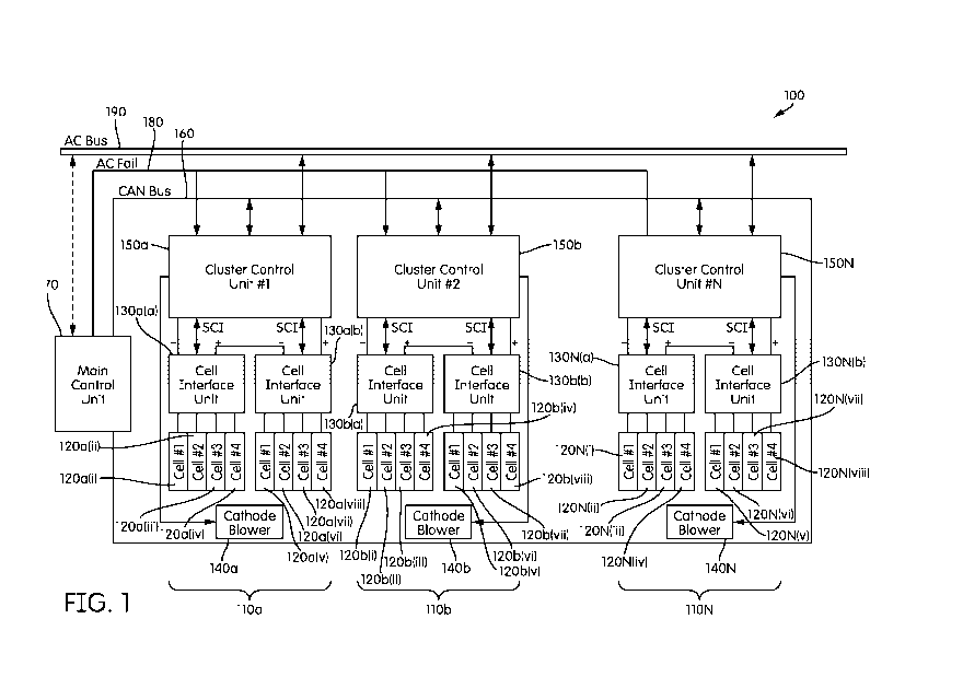
[0011] Figure
1 depicts a schematic view of an electrochemical cell system having a
plurality of modules, each containing a plurality of electrochemical cells
therein; and
[0012] Figure
2 depicts a schematic control diagram of a control circuit associated
with each module, configured to perform droop compensation for an associated
module
relative to other modules in the electrochemical cell system of Figure 1.
DETAILED DESCRIPTION
[0013] Figure
1 illustrates a schematic view of an electrochemical cell system 100.
In the illustrated embodiment, the electrochemical cell system 100 includes a
plurality of
cell modules 110 (individually cell modules 110a, 110b, and 110N ¨ N being an
integer
of 3 or more), each including a plurality of electrochemical cells therein. It
may be
appreciated that the electrochemical cell system 100 may include any
appropriate number
of cell modules 110 therein (e.g., two or more). In various embodiments, the
cell modules
110 may include a different number of electrochemical cells 120 therein. In
the illustrated
embodiment, each module 110 includes eight electrochemical cells 120
(specifically,
electrochemical cells 120a(i-viii) in cell module 110a, electrochemical cells
120b(i-viii)
in cell module 110b, and electrochemical cells 120N(i-viii) in cell module
110N).
[0014] In an
embodiment the electrochemical cells 120 of each cell module 110 may
be subdivided into two interface groups, each having an associated cell
interface unit 130.
As shown, cell interface unit 130a(a) may group cells 120a(i)-(iv), while cell
interface
unit 130a(b) may group cells 120a(v)-(viii). Similarly, cell interface unit
130b(a) may
group cells 120b(i)-(iv), while cell interface unit 130b(b) may group cells
120b(v)-(viii).
Furthermore, cell interface unit 130N(a) may group cells 120N(i)-(iv), while
cell
3
CA 02886246 2015-03-25
WO 2014/052773
PCT/US2013/062208
interface unit 130N(b) may group cells 120N(v)-(viii). In an embodiment, the
cell
interface units 130 may liffl( the cells 120 associated therewith in series.
Additionally, the
cell interface units 130 may themselves be linked in series. As such, the
voltage of each
of the cells 120 in a given cell module 110 may add up. In the illustrated
embodiment,
with eight electrochemical cells 120 in each cell module 110, if each
electrochemical cell
110 supplies 1VDC volt, then the eight cells 120 in series may supply 8VDC. It
may be
appreciated that different cell modules 110 may supply different voltages
(e.g., one cell
module supplies 8VDC, while another supplies 6VDC).
[0015] While
the electrochemical cells 120 may vary across embodiments, in some
embodiments one or more of the cells 120, and/or other features of the
electrochemical
cell system 100, may include elements or arrangements from one or more of U.S.
Patent
Application Serial Numbers 12/385,217 (issued as U.S. Patent 8,168,337),
12/385,489
(issued as U.S. Patent 8,309,259), 12/549,617 (issued as U.S. Patent
8,491,763),
12/631,484, 12/776,962, 12/885,268, 13/028,496, 13/083,929, 13/167,930,
13/185,658,
13/230,549, 13/299,167, 13/362,775, 13/531,962, 13/532,374 13/566,948, and
13/668,180, each of which are incorporated herein in their entireties by
reference. That is,
the cells (and the system made up of those cells) may be a rechargeable power
source
(also referred to as secondary cells), which may be charged by an external
power source
(e.g., solar cells, wind turbines, geothermally generated electricity,
hydrodynamically
generated electricity, engine/brake generated electricity, the main power
grid, etc.) and
discharged as needed/desired (e.g., as back-up power, to discharge stored
power, in lieu
of a fossil fuel engine, etc.).
[0016] In some
embodiments the cell interface units 130 may be configured to
monitor the status of each cell 120 associated therewith, and may provide
switching or
other functionality configured to isolate or otherwise bypass faulty cells
120, such as is
described in U.S. Patent Application No. 13/299,167, incorporated by reference
above.
As another example, in embodiments where one or more of the electrochemical
cells 120
are metal-air cells, the cells 120 may be utilized at least in part to power a
cathode
blowers 140 (individually cathode blowers 140a, 140b, and 140N as illustrated)
associated with the cell modules 110, which may be configured to direct a flow
of air or
other oxidant to oxidant electrodes associated with each of the cells 120, as
described in
4
CA 02886246 2015-03-25
WO 2014/052773
PCT/US2013/062208
U.S. Patent Application 13/531,962, entitled "Immersible Gaseous Oxidant
Cathode for
Electrochemical Cell System," incorporated by reference in its entirety above.
[0017] For
each module 110, a cluster control unit 150 (individually cluster control
units 150a, 150b, and 150N in the illustrated embodiment) links the cell
interface units
130, and provides programmatic control thereof via a serial communications
interface
(SCI) associated with each. The cluster control units 150 may be linked to
each other
through a Controller Area Network (CAN) Bus 160. Programmatic or other control
of the
cell modules 110 may be provided from a main control unit 170, which may also
be
linked to the CAN Bus 160. Embodiments of such programmatic control are
described in
greater detail below. In some embodiments, such as that illustrated, an AC
Fail circuit
180 may also be implemented in the electrochemical cell system 100, and may be
coupled to the main control unit 170 and each of the cluster control units
150. The AC
Fail circuit 180 may be configured to direct the cluster control units 150 of
the cell
modules 110 to supply power to an AC Bus 190 on an as-needed basis. For
example, if
AC power on the grid fails, the AC Fail circuit 180 may be configured to draw
power
from the electrochemical cells 120. It may be appreciated that in some
embodiments the
AC Bus 190 may generally receive DC power from the cell modules 110, however
may
be associated with an inverter configured to convert the DC power to AC power.
In other
embodiments, each cell module 110 may include one or more inverters,
configured to
supply AC voltage across the AC Bus 190. In some embodiments, the AC Bus 190
may
be coupled to the main control unit 170 (e.g., through any appropriate sensor
or sensing
system), as illustrated by the dashed line therebetween in Figure 1. In an
embodiment, the
main control unit 170 may control an inverter associated with the AC bus 190.
In some
embodiments, the functions of the AC Fail circuit 180 may be combined with the
CAN
Bus 160, or any other appropriate another control link.
[0018] It may
be desirable to perform droop compensation in the electrochemical
cell system 100, so as to facilitate equalization of currents, which may
correspondingly
equalize a lifecycle of the cell modules 110 and the electrochemical cells 120
therein. By
equalization of currents, it may be understood that the droop compensation may
facilitate
generally or essentially equalizing the currents (e.g., driving the currents
towards
equalization, into a state generally regarded in the art as being equalized).
In an
CA 02886246 2015-03-25
WO 2014/052773
PCT/US2013/062208
embodiment, droop compensation may be performed utilizing a control circuit
associated
with a controller in each cluster control unit 150. As such, in some
embodiments droop
compensation may be performed on a cell module by cell module basis. In other
embodiments, droop compensation may be performed among subsets of the cell
modules
110, such as by being implemented at the level of the cell interface units
130. In still
other embodiments, droop compensation may be performed on a cell by cell
basis, being
implemented associated with each individual electrochemical cells 120. Other
implementations are also possible.
[0019] Figure
2 illustrates a control block diagram for a control circuit 200
illustrating an example of how droop compensation may be implemented (e.g., on
the
electrochemical cell system 100) according to an embodiment. In the
illustrated
embodiment, the control circuit 200 shows that the control scheme operates on
a
conversion from a boost input voltage 210 to a boost output voltage 220, via a
boost
circuit 225 (i.e., a converter), described in greater detail below. In the
example illustrated,
the boost input voltage 210 is shown as being 8VDC nominal. It may be
appreciated that
such an input voltage may result from the summation in series of each of the
eight
electrochemical cells 120 associated with each electrochemical cell module
110,
outputting 1VDC each. Additionally, as shown, in an embodiment the boost
output
voltage 220 may be stepped up (i.e., amplified) to 52VDC nominal by the boost
circuit
225. In the example illustrated, the 52VDC 42VDC
range may be based on telecom
requirements, wherein all loads are active at 52VDC, noncritical loads (NCL)
drop out at
48VDC, and only critical loads (CL) are kept active around 42-45VDC. While
having a
CL voltage range instead of a fixed value is uncommon, the range may be based
on any
customer desired range. It may be appreciated that one could adjust scaling
factors to
accommodate the ranges. As described in greater detail below, the
amplification of the
boost circuit 225 may be variable, so as to provide the desired droop
compensation. In an
embodiment, the boost output voltage 220 may be output to the AC Bus 190 of
the
electrochemical cell system 100.
[0020] In an
embodiment, to perform the droop compensation using the control
circuit 200, a fixed reference voltage 230 is received at a first summation
junction 240. In
the illustrated embodiment, the fixed reference voltage 230 is 5VDC. It may be
6
CA 02886246 2015-03-25
WO 2014/052773
PCT/US2013/062208
appreciated that the 5VDC may be an exemplary scaling point, and could be
anywhere
from 1VDC to 10VDC in some embodiments, depending on nominal board operating
voltage. The fixed reference voltage 230 may be provided by any appropriate
source,
including, for example, ultimately from one or more of the electrochemical
cells 120, or
from a separate power source. At the first summation junction 240, the fixed
reference
voltage 230 may have a first voltage modifier 250 subtracted therefrom. As
described in
greater detail below, the first voltage modifier 250 may be computed from a
sensed
current (I) associated with the boost input voltage 210. A software voltage
adjustment
260 may also be applied at the first summation junction 240, also being
subtracted from
the fixed voltage reference 230. In some embodiments, the software voltage
adjustment
260 may be computed or otherwise derived from properties of the cell, or may
be
received as a user input. In an embodiment, the software voltage adjustment
260 may
range from OV to 0.962V, as described in greater detail below. It may be
appreciated that
the value 0.962 may be calculated as a scaling factor based on the 5VDC
reference.
When the scaling factor is at zero, boost output voltage is 52VDC. When the
scaling
factor is at 0.962, however, the boost output voltage is 42VDC. The adjustment
alteration
may be based on user control of what loads are active (i.e. critical loads,
non-critical
loads). The value may be any number and is only dependent the boost output
voltage
range desired. The summation of the fixed reference voltage 230, minus the
software
voltage adjustment 260 and the first voltage modifier 250, may be output as a
voltage
reference 270.
[0021] The
voltage reference 270 may be input into a second summation junction
280. At the second summation junction 280, a second voltage modifier 290 may
be
subtracted from the voltage reference 270. As shown in the illustrated
embodiment, the
second voltage modifier 290 may be computed based on the boost output voltage
220,
which may form a PI loop (i.e., a proportional-integral loop, wherein the
control circuit
200 comprises a PI controller). In particular, in an embodiment, the boost
output voltage
220 may be fed into a step down op-amp 300, which in the exemplary embodiment
of
Figure 2, has a gain of 0.096. This is so in the illustrated embodiment
because the boost
output voltage 220 is nominally 52VDC, while the fixed reference voltage 230
is 5VDC
(52VDC * 0.096 z 5VDC).
7
CA 02886246 2015-03-25
WO 2014/052773
PCT/US2013/062208
[0022] If
there were no load associated with the boost output voltage 220, then there
would be no current associated with the boost input voltage 210. As such, the
first
voltage modifier 250 associated with the lack of a sensed current would be
zero, and
(absent any software voltage adjustment 260) the voltage reference 270 would
be the
same as the fixed reference voltage 230. With the gain of the step down op-amp
300
being associated with the fixed reference voltage 230, in such a situation the
voltage
reference 270 would be equal to the second voltage modifier 290, resulting in
an error
output 310, i.e., e(t), of zero. It may be appreciated that where the boost
output voltage
220 drops, the second voltage modifier 290 also drops, creating a non-zero
error output
310. As described in greater detail below, the error output 310 may be
utilized to modify
the amplification of the boost circuit 225 from the boost input voltage 210 to
the boost
output voltage 220, to compensate for the change.
[0023] When a
load is applied to the boost output voltage 220, the first voltage
modifier 250, associated with a current associated with the boost input
voltage 210, may
adjust the voltage reference 270. Specifically, with the addition of a load,
the current
associated with the boost input voltage 210 may increase from zero to a
positive value.
As shown in Figure 2, to detect the current of the boost input voltage 210,
the boost
circuit 225 may include therein a current sensor 320. In an embodiment, a wire
carrying
the boost input voltage 210 may be run through the current sensor 320, which
may pick
up an associated magnetic field associated therewith, and output an inductor
current
measurement 325 that is proportional to the magnetic field. The current may be
measured
by the current sensor 320 as amperes (A). Such an ampere inductor current
measurement
325 may be converted into a voltage reading by a current to voltage converter
330 (as the
controls implemented in the control circuit 200 may generally operate in
voltages). The
inductor current measurement 325, as converted to a voltage, may then be fed
back
through the control circuit 200 to establish the first voltage modifier 250,
described
above. It may therefore be appreciated that because the first voltage modifier
250 is
utilized in establishing the voltage reference 270, the inductor current
measurement 325
is also utilized to establish the error output 310. In some embodiments, the
current sensor
320 may sense current by other means besides induction. For example, a current
sense
resistor may be employed with known precision resistance.
8
CA 02886246 2015-03-25
WO 2014/052773
PCT/US2013/062208
[0024] As
shown, the error output 310 is utilized to establish a current reference 335
(i.e., "I-ref") for the control circuit 200. It may be appreciated that in
some embodiments
the system implementing the control circuit 200 (e.g., the system 100) may
have a current
limit of 40ADC. Such a current limit may correspond to a 2.5VDC limit in the
control
circuit 200. It may be appreciated that the 40ADC limit may be by user
requirement, and
may be a protection limit so, for example, if customer load sources more than
40A out of
module, this will limit input current from modules. If bus is shorted, 40A
limit will
clamp, thus only allowing 40A for protection purposes. The example selection
of a 2.5V
limit in the illustrated embodiment is user selected, and in some embodiments
could
range from approximately 1V to 10V. If bus is overloaded (e.g., a shorted out
bus), the
output voltage is forced to zero, and the error output will saturate. The
saturated error
output may command I-ref to go high (however capped by the limit). As an
example,
with a current swing or a customer demand of 40A, the boost output voltage
will go
below 52VDC, but it is desirable to stay above 48VDC so as not to drop out
critical loads
CL. Accordingly, when input current is 40A, the 480 mV value may be scaled
from the
5VDC exemplary selection, similar to the software adjustments. In the
illustrated
embodiment, the error output 310 associated with the voltage reference 270
passes
through a voltage limiter 340, which limits the error output 310 to 2.5V,
corresponding to
40ADC. The error output 310, as limited by the voltage limiter 340, may be
considered
the current reference 335. Similarly, because a 40A limit may exist for the
measurement
of the current sensor 320, the current to voltage converter 330 may also
correspond to a
limit of 2.5V, which amounts to 62.5mV/A. A step down op-amp 350 having a gain
or
0.192 may reduce the influence of the inductor current on the control circuit
200 to
12mV/A (480mV = 40ADC). In some embodiments, the reduced voltage associated
with
the inductor current may then be fed into a timing delay 360. In the
illustrated
embodiment, the timing delay 360 may be for 100ms. Other time delays are also
possible
in other embodiments. It may be appreciated that the timing delay 360 may be
configured
to slow down the operation of the control loop, which may dampen out the loop
of the
control circuit 200, to prevent high oscillation before achieving stability,
as described in
greater detail below. It may be appreciated that some embodiments might not
include a
timing delay 360, but might include other mechanisms to prevent undesirable
oscillation
9
CA 02886246 2015-03-25
WO 2014/052773
PCT/US2013/062208
of the loop of the control circuit 200.
[0025] The
reduced voltage associated with the inductor current, which in the
illustrated embodiment results from the step down op-amp 350, and may be time
delayed
by the timing delay 360, may thus be fed back into the first summation
junction 240 as
the first voltage modifier 250, which determines the voltage reference 270.
Having
utilized the inductor current to establish the error output 310 associated
with the voltage
reference 250, the inductor current may then be utilized to establish an error
output 370
associated with the current reference 335. Specifically, the current reference
335,
established based on the voltage reference 270 and the reduced boost output
voltage 220
(as the second voltage modifier 290) may be adjusted at a third summation
junction 380.
In an embodiment the inductor current measurement 325, converted to a voltage
by the
current to voltage converter 330, may be subtracted directly from the current
reference
325. In other embodiments, such as that illustrated, a fourth summation
junction 390 may
allow the inductor current measurement 325, as converted to a voltage, to be
modified by
a software current adjustment 400. In some embodiments, the software current
adjustment 400 may be computed or otherwise derived from properties of the
cell, or may
be received as a user input. In an embodiment, the software current adjustment
400 may
be measured as a voltage, and may be between 0 and 2.5V, corresponding to
being
between 0 and 40ADC, as described above. Regardless, by subtracting the
inductor
current measurement 325 (e.g., as converted to voltage by the current to
voltage converter
330, and potentially as modified by the software current adjustment 400) from
the current
reference 335, the error output 370 associated with the current reference 335
may be
computed. The error output 370 may then be received by the boost circuit 225,
and may
determine an error input for a pulse width modulator 410 thereof. The pulse
width
modulator 410 may be configured to dictate how much current is drawn by the
boost
circuit 225, and may be tied into the boost circuit 225 in such a manner so as
to modify
the boost amplification from the boost input voltage 210 to the boost output
voltage 220,
as described below.
[0026] Because
the boost output voltage 220 is fed back through the control circuit
200 in a manner that in part determines the error output 310 associated with
the reference
voltage 270, and because that boost output voltage 220, in conjunction with
the load
CA 02886246 2015-03-25
WO 2014/052773
PCT/US2013/062208
demands, varies the current supplied in the boost input voltage 210 (sensed by
the current
sensor 320 as inductor current 325), which is fed back to determine at least
in part the
voltage reference 270 and the current reference 335, it may be understood that
the boost
circuit 225 as a whole will modulate the boost in response to current demands
associated
with the load coupled to the boost output voltage 220. With multiple boost
circuits 225
coupled to a common load, where each is controlled by control schemes such as
that
found in the control circuit 200, the boost circuits 225 are independent from
one another
in their operation, however may respond to one another through the demands of
the load
on the associated boost output voltages 220. The operation of this
responsiveness is
discussed below.
[0027] It may be appreciated that the cell or cells associated with
whichever one of
the boost circuits 225 is outputting a greatest boost output voltage 220 would
initially
attempt to supply all of the power to the load. The effect of that boost
circuit 225
attempting to supply all of the power to the load would be an associated
increase in the
inductor current, as discussed above. The increase in inductor current then
causes the
control circuit 200 to droop the boost output voltage 220 for that boost
circuit 225. Once
the boost output voltage 220 from the boost circuit 225 falls below that of a
second boost
circuit 225 (having what was previously the second highest boost output
voltage 220) the
second boost circuit 225 would then itself attempt to supply all of the power
to the load.
This would cause the second boost circuit 225 to droop its boost output
voltage 220. The
process would then repeat, creating a cycle where the boost circuits 225 and
associated
cells attempt to supply all of the power to the load, and the output voltages
"droop" in
response, which causes other boost circuits 225 and associated cells to
continue the cycle.
It may be appreciated that the amount by which the boost circuit 225 droops
the boost
output voltage 220 depends on the error output 370 established based on the
current
reference 335. For example, where the current reference 335 saturates at the
40A limit,
the boost circuit 225 may droop the boost output voltage 220 close to zero to
compensate.
[0028] Through the cycle, the different boost circuits 225 and associated
cells may
oscillate as to which is attempting to fully power the load. Eventually, all
boost circuits
225 would trend towards a stable equilibrium, where each of the boost circuits
225 have
the same boost output voltage 220 and similarly, have the same current
reference 335.
11
CA 02886246 2015-03-25
WO 2014/052773
PCT/US2013/062208
Even though the current reference 335 will be driven towards equalization
across all
controllers, the output current from the boost circuits 225 (e.g., associated
with the boost
output voltages 220, and coupled in parallel to the load) may be different for
each
converter. Accordingly, the current associated with the boost input voltage
210 (e.g., as
measured by the current sensor 320 as the input inductor current 325) would
also be
driven towards equalization by the boost circuit 225. It may be appreciated
that the
equalization of currents, and the common boost output voltage 220 across
different cells
or cell modules, is independent of the boost input voltage 210 obtained from
the cell or
cell modules.
[0029] Such
independent ability of each cell or module to attempt to equalize current
may be beneficial to enhance performance and lifespan of the cells of the
system. To
apply this understanding in the context of the system 100 in Figure 1, if the
control
schemes of the control circuit 200 are implemented in each of the cluster
control units
150, a load associated with the AC Bus 190 may cause the cluster control units
150 to
react to one another, varying the amplification of the boost circuits 225
associated with
each to attempt to equalize current demands across the cell modules 110. Thus,
if the cell
module 110a initially has the highest boost output voltage 220 being output to
the AC
Bus 190, the electrochemical cells 120a(i-viii) would attempt to supply all of
the power
to the load, and the current sensor 320 would identify the increased current
associated
therewith. The sensed current would be fed back through the control circuit
200 of the
cell module 110a, causing the boost circuit 225 of the cluster control unit
150a to droop
the amplification to supply a smaller boost output voltage 220. If cell module
110b
subsequently has the greatest boost output voltage 220, then the
electrochemical cells
120b(i-viii) would attempt to supply all of the power to the load via the AC
Bus 190,
causing a corresponding increase in the current sensed in the cluster control
unit 150b.
The current would be fed back through the control circuit 200 of the cluster
control unit
150b, causing the boost circuit 225 to similarly droop the amplification. This
may occur
through the boost circuits 225 associated with each of the cluster control
units 130 of the
cell modules 110, until each of the boost circuits 225 achieve a stabilization
point, with
generally equal current being drawn by the cell modules 110.
[0030] It may
be appreciated that the boost circuit 225 may vary across
12
CA 02886246 2015-03-25
WO 2014/052773
PCT/US2013/062208
embodiments, and may be of any appropriate configuration. Boost circuits 225
typically
include two or more semiconductor switches. For example, in the illustrated
embodiment
the boost circuit 225 includes a Field Effect Transistor (FET) 420, and a
diode 430. The
FET 420 opens and closes according to a duty cycle 440 (i.e., "D") provided by
the pulse
width modulator 410. Boost circuits 225 may further include one or more energy
storage
elements. In the illustrated embodiment, the boost circuit 225 includes an
input inductor
450, and a pair of capacitors 460. In operation, the switching of the FET 420,
in
conjunction with the stored energy in the input inductor 450 and the
capacitors 460,
results in the boost output voltage 220 being greater than the boost input
voltage 210,
with the amount of amplification, in the present embodiment, being variable
depending
on the duty cycle 440 from the pulse width modulator 410.
[0031] It may
be appreciated that the control circuit 200 may be implemented in a
variety of systems, including but not limited to system 100 of Figure 1.
Further, the
source of the boost input voltage 210 may vary across embodiments. While in
the
illustrated embodiment eight cells (e.g., 120N(i-viii)) are electrically
coupled together in
series to provide an 8VDC source for the boost input voltage 210, in other
embodiments,
the control circuits 200 may be implemented on individual electrochemical
cells 120
(e.g., such that the boost input voltage 210 is 1VDC). It may further be
appreciated that
the cell modules 110 and/or the electrochemical cells 120 therein may vary
across
embodiments.
[0032] As
noted above, in some embodiments, the electrochemical cells 120 may
include features from those listed applications incorporated by reference
herein. For
example, in some embodiments the electrochemical cells 120 may include a
plurality of
permeable electrode bodies. In some embodiments the plurality of permeable
electrode
bodies may be configured to be electrically connected to one another through
charging of
the electrochemical cell 120. In some embodiments the permeable electrode
bodies may
be selectively coupled to either an anode or a cathode in the electrochemical
cell 120
during charging of the electrochemical cell 120, so as to form a plurality of
electrochemical cells within each electrochemical cell 120 (e.g., by
alternatively
associating different permeable electrode bodies with the anode and the
cathode, so that
fuel grows on some of the permeable electrode bodies towards others of the
permeable
13
CA 02886246 2015-03-25
WO 2014/052773
PCT/US2013/062208
electrode bodies).
[0033]
Likewise, during discharge of the cells 120, in some embodiments, the
external load associated with the AC Bus 190 may only be coupled to the
terminal
permeable electrode body, distal from an oxidant reduction electrode of each
electrochemical cell 120, so that fuel consumption may occur in series from
between each
of the permeable electrode bodies. In other embodiments, the external load may
be
coupled to some of the electrode bodies in parallel, as described in detail in
United States
Patent Application Serial No. 12/385,489, incorporated above by reference. In
some
embodiments, a switching system such as that described in U.S. Patent
Application Serial
No. 13/299,167, incorporated above by reference, may facilitate selective
electrical
connections between the permeable electrode bodies. In some embodiments, the
cells
may be configured for charge/discharge mode switching, as is described in
United States
Patent Application Serial No. 12/885,268, incorporated by reference above.
[0034] In some
embodiments including a switching system, switches associated
therewith may be controlled by a controller, which may be of any suitable
construction
and configuration. In the system 100 of Figure 1, such controllers may be
associated with
each cell 120, each cell interface unit 130, each cluster control unit 150, or
with the main
control unit 170. In some embodiments, the controllers may have a hierarchal
association
with one another, such that a more superior controller (e.g., in the main
control unit 170)
may transmit commands to lower controllers (e.g., in the cluster control units
150). In
some embodiments, one or more of the controllers may include features
conforming
generally to those disclosed in U.S. Application Serial Numbers 13/083,929,
13/230,549
and 13/299,167, incorporated by reference above. In various embodiments, the
control of
the switches of a switching system may be determined based on a user
selection, a sensor
reading, or by any other input. In some embodiments, the controller(s) may
also function
to manage connectivity between the load and the AC Bus 190, or may selectively
supply
power (e.g., over the AC Bus 190) to the electrochemical cells 120 for
recharging thereof
As noted above, in some embodiments, the controller may include appropriate
logic or
circuitry for actuating bypass switches associated with each electrochemical
cell 120
coupled in the cell interface units 130 or otherwise in the cell modules 110,
in response to
14
CA 02886246 2015-03-25
WO 2014/052773
PCT/US2013/062208
detecting a voltage reaching a predetermined threshold (such as drop below a
predetermined threshold).
[0035] The
foregoing illustrated embodiments have been provided solely for
illustrating the structural and functional principles of the present invention
and are not
intended to be limiting. For example, the present invention may be practiced
using a
variety of fuels, oxidizers, electrolytes, and/or overall structural
configurations or
materials. Thus, the present invention is intended to encompass all
modifications,
substitutions, alterations, and equivalents within the spirit and scope of the
following
appended claims.