Note: Descriptions are shown in the official language in which they were submitted.
CA 02886331 2015-03-25
WO 2014/049593 PCT/1L2013/050790
SYSTEM AND METHOD FOR COUPLING PROXIMITY IC CARD/MODULE TO
PROXIMITY COUPLING DEVICE IN LOW MUTUAL MAGNETIC COUPLING
CONDITIONS
BACKGROUND OF THE INVENTION
[001] Proximity Integrated Circuit Card (PICC) is widely used for
communicating information
to/from respective card reader devices in variety of applications. Proper
operation of PICC devices
with a respective card reader depends highly on the level of mutual magnetic
coupling that is
established between the card and the reader. This level is first of all
dictated by geometrical aspects
(relative sizes, distance and orientation between the antennas of the PICC and
the reader) and
to secondly by the usually adverse effects of conductive (or semi
conductive) objects which are present
in the close vicinity of the two antennas. The induced circulating current in
such objects both absorb
part of the magnetic field energy and distort the three dimensional shape of
the magnetic field, with
the effect of reducing the level of the mutual magnetic coupling. Additional
similar adverse effect is
associated with the presence of materials which absorb the reader magnetic
field due to its high
"imaginary" permeability at the reader carrier frequency. The worst case
effect is when such objects
are present between the PICC and reader antennas.
[002] In some embodiments, especially when the PICC is placed inside mobile /
cellular /
smartphone device, there is a need to position the PICC so that between it and
a card reader there
are conductive-absorbing materials such as metal cover, battery, etc. The
establishment of a
communication channel between the PICC and the card reader, herein after
coupling, typically
requires first that the PICC will receive enough RF energy from the card
reader to enable proper
operation of the PICC and second that for the data communication back from the
PICC to the card
reader, the PICC is able to produce strong enough response signal so as to
enable the card reader to
identify the signal and decode its data content. The PICC response to the card
reader is affected by
means of load modulation. The PICC changes-modulates the loading condition of
its antenna, which
is picked up by the card reader by means of the mutual coupling between the
two antennas. When
the PICC antenna is located so that such conductive and/or absorbing objects
are placed between it
and the card reader, the change in load may be too small to be noticed by the
card reader. This
adverse effect becomes the major issue if the PICC power supply issue is
resolved by alternative
means (e.g. power supply from its host mobile / cellular / smartphone device).
The reduced
magnetic coupling usually is not considered critical for the data transmission
from the card reader to
t
CA 02886331 2015-03-25
WO 2014/049593 PCT/1L2013/050790
the PICC due to the much higher level of this signal compared with the load
modulation signal back
from the PICC to the card reader.
[003] Reference is made to Fig. 1 schematically presents a PICC 20 located
within a host device
10, such as mobile / cellular / smartphone device. PICC 20 may be located so
that between it and the
closest wall of device 10 are located conductive and/or absorbing elements,
such as battery 14 and
metallic outer wall 12. Coupling of PICC 14 with card reader 50 involves
transmission of RF signal
52 from card reader 50 to PICC 20 and transmission of RF signal 54 from PICC
20 to card reader
50.
[004] There is a need to enable the PICC to affect strong enough data signal
to the card reader to
to overcome the low mutual magnetic coupling. That need cannot be fulfilled
by means of the standard
load modulation as the signal received card reader 50 is too low in such
cases.
SUMMARY OF THE INVENTION
[005] A proximity integrated circuit card (PICC) comprising a main loop
antenna to transmit data
from said PICC and a secondary loop antenna to receive RF transmission to said
PICC, said main
antenna and said secondary antenna arranged to yield low mutual magnetic
coupling so that said RF
transmission to said PICC yields bigger signal in said secondary antenna than
the signal yields in
said secondary antenna from a transmission from said main antenna. According
to some
embodiments secondary antenna is arranged to only partially overlaps said main
antenna.
[006] A proximity integrated circuit card (PICC) comprising a main antenna to
transmit data from
said PICC and to receive RF transmission to said PICC, wherein said main
antenna is to receive said
RF transmissions during times when said main antenna does not transmit,
wherein at the end of a
transmit period said PICC forces a decay on said main antenna for a decay
period of time, and
wherein said main antenna is to begin receiving of said RF transmission only
after said decay
period.
[007] A method for transmitting and receiving RF transmissions in a proximity
integrated circuit
card (PICC) having only one transmit and receive antenna comprising
transmitting RF transmission
signal from said antenna for a transmit period of time, forcing decay of said
RF transmission signal
at the end of said transmission period for a decay period of time and
receiving RF transmission
signal only after the end of said decay period of time.
2
CA 02886331 2015-03-25
WO 2014/049593 PCT/1L2013/050790
BRIEF DESCRIPTION OF THE DRAWINGS
[008] The subject matter regarded as the invention is particularly pointed out
and distinctly
claimed in the concluding portion of the specification. The invention,
however, both as to
organization and method of operation, together with objects, features, and
advantages thereof, may
best be understood by reference to the following detailed description when
read with the
accompanying drawings in which:
[009] Fig. 1 schematically presents a PICC located within a host device, such
as mobile / cellular /
smartphone device;
[0010] Fig. 2 schematically presents a PICC located within a host device, such
as mobile / cellular /
to smartphone device, according to embodiments of the present invention;
[0011] Fig. 3 schematically presenting a PICC, according to embodiments of the
present invention;
[0012] Fig. 3A schematically presenting decoupling arrangement of a PICC
transmitting coil and
PICC pickup coil according to embodiments of the present invention;
[0013] Fig. 4A schematically presents a PICC according to yet other
embodiments of the present
invention; and
[0014] Fig. 4B schematically presenting timing schemes and wave forms of
transmitted signal and
received signal from/to a PICC according to embodiments of the present
invention.
[0015] It will be appreciated that for simplicity and clarity of illustration,
elements shown in the
figures have not necessarily been drawn to scale. For example, the dimensions
of some of the
elements may be exaggerated relative to other elements for clarity. Further,
where considered
appropriate, reference numerals may be repeated among the figures to indicate
corresponding or
analogous elements.
DETAILED DESCRIPTION OF THE PRESENT INVENTION
[0016] In the following detailed description, numerous specific details are
set forth in order to
provide a thorough understanding of the invention. However, it will be
understood by those skilled
in the art that the present invention may be practiced without these specific
details. In other
instances, well-known methods, procedures, and components have not been
described in detail so as
not to obscure the present invention.
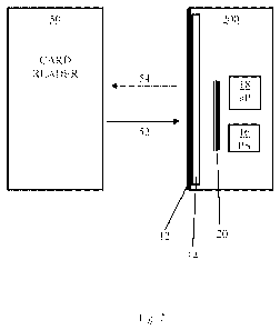
[0017] Reference is made now to Fig. 2, which schematically presents a PICC 20
located within a
host device 200, such as mobile / cellular / smartphone device, according to
embodiments of the
present invention. PICC 20 may be located, similarly to PICC of Fig. 1, so
that between it and the
closest wall of device 200 are located conductive and/or absorbing elements,
such as battery 14 and
3
CA 02886331 2015-03-25
WO 2014/049593 PCT/1L2013/050790
metallic outer wall 12. Coupling of PICC 14 with card reader 50 involves
transmission of RF signal
52 from card reader 50 to PICC 20 and transmission of RF signal 254 from PICC
20 to card reader
50. Further, PICC 20 may be powered from power supply unit 16 of host device
200. Optionally,
PICC 20 may be in active communication with uP 18 of host device 200, for
example in order to
receive data from PICC 20 and to provide data and / or control commands to
PICC 20. It will be
noted that PICC 20 may comprise a controller (CPU, microcontroller, etc.)
inside it (not shown) as
is known in the art, which is adapted to control the operation of PICC 20
according to the applicable
operation scheme(s). At least two coupling difficulties may arise due to the
low mutual magnetic
coupling conditions in host device 200. First is low magnitude of received RF
signal 52, which may
bee too low to support proper operation of PICC 20. Second is low magnitude of
sent signal 254
from PICC 20 to card reader 50, again, due to the low mutual magnetic coupling
conditions in host
device 200. As a result signal 254 may be too low to enable proper coupling,
for example, in load
modulation coupling mode. According to embodiments of the present invention
instead of
powering PICC 20 by RF signal 52 transmitted by card reader 50 PICC 20 in host
device 200 may
be powered by power supply unit 16, thus overcoming the too low received RF
power of signal 254
through the conductive and/or absorbing medium of metallic cover 12 and
battery 14.
[0018] However, powering PICC 20 from power supply unit 16 of host device 200
may not suffice,
since load modulation signal picked by card reader 50 may still be too low.
According to
embodiments of the present invention instead of coupling PICC 20 to card
reader 50 using load
modulation signal, which is considered a passive approach, PICC 20 may be
adapted to transmit
active signal which is synchronized with card reader 50 transmitted carrier
signal. According to
embodiments of the present invention PICC 20 may transmit a carrier signal 254
at exactly the same
frequency and with basically none changing phase difference compared with the
card reader 50
transmitted carrier signal. This carrier signal is modulated by the PICC data
so as to resemble, from
the card reader point of view, the load modulation signal of standard PICCs.
To that effect it may be
modulated by the standard 848KHz subcarrier . The sub carrier modulated signal
may carry (be
modulated by) the same data commonly transmitted by PICC 20 for example using
load modulation
coupling mode.
[0019] In order for the card reader to pick up the active PICC transmission
signal 254 in the same
manner as standard load modulation that PICC signal 254 need to be at exact
same frequency of the
card reader transmitted signal 52. Even the phase difference between the two
signals (52 and 254)
has to stay constant (within certain limits) for the whole duration of the
PICC message, to refrain
from corrupting the PICC transmitted data, decoded by the card reader. Such
precise
4
CA 02886331 2015-03-25
WO 2014/049593 PCT/1L2013/050790
synchronization requires the PICC to pick up the card reader signal as
reference at least during
certain periods inside the PICC message period. According to one embodiment of
the present
invention the PICC may be equipped with two coils. Reference is made now to
Fig. 3, schematically
presenting PICC 300, according to embodiments of the present invention. PICC
300 may comprise
at least card controller 302 in active communication with transmit antenna
coil 312 adapted to
transmit signals from PICC 300 to a card reader (not shown) and receive
antenna coil 314 (also
called pickup coil) adapted to receive transmission signal 334 from the card
reader. An RF isolation
arrangement 320 may be provided to magnetically decouple coils 312 and 314
from one another in
order to enable coil 314 to receive transmissions signals from the card reader
(in order to provide
synch timing) concurrently with the transmissions of coil 312, without
interfering with each other.
Such isolation arrangement typically involves the use of ferrite materials.
The ability to perform the
required "listen-while-talk" function depends highly on the magnetic
decoupling provided by
isolator element 320.
[0020] Reference is made now to Fig, 3A, schematically presenting decoupling
arrangement of
transmitting coil 312 and pickup coil 314, according to embodiments of the
present invention.
Pickup coil 314 may be placed over transmitting coil 312, partly inside of it
and partly outside. Both
geometries should be fine tuned to achieve maximum cancelation of the mutual
coupling. One main
problem in using this solution may be the effect of the metallic environments
included in at least
some of the host devices models, which may differ from one host device model
to another, on the
mutual coupling and the fine tuning mentioned above should consider this
effect. Ferrite layer
and/or well-placed metallic layer(s) 360 may reduce the effect inflicted by
the various metallic
environments of various host devices on the mutual coupling. In addition a
special circuitry may be
designed to inject a controlled and calibrated amount of PICC carrier into the
pickup circuitry of
coil 314 in anti phase to the coupled transmission phase in coil 312 so as to
further reduce this
coupling. The amount of injected signal may be calibrated while running PICC
300 without the
presence of an active card reader so as to make sure the cancelation
adjustment does not cancels the
card reader signal.
[0021] According to another embodiment of the present invention a PICC may
perform active
synchronization using only a single transmit/receive coil. Reference is made
now to Fig. 4A,
schematically presenting PICC 400 according to embodiments of the present
invention and to Fig.
4B, schematically presenting timing schemes and wave forms of an envelope of
transmitted signal
432A and an envelope of received signal 432B from/to PICC 400, according to
embodiments of the
present invention. PICC 400 may comprise at least controller unit 402 powered,
for example, from
5
CA 02886331 2015-03-25
WO 2014/049593 PCT/1L2013/050790
power supply unit of the host device and in active communication with
transmit/receive antenna coil
412. Coil 412 may be controlled to switch from receive to transmit and vise
versa by controller unit
402.
[0022] The transmitted signal 432A from PICC 400 to a card reader is expected
to be much larger
than the picked-up signal 432B received by PICC 400 from the card reader.
Therefore, a forced very
fast decay of the transmitted signal may be activated for short time td at the
beginning of each off
period ToFF. Such forced decay may be realized for example by shorting the
antenna upon
deactivation of the transmitter, allowing the coil stored energy to dissipate
in the shorting switch.
This may be embodied, for example, utilizing an FET transistor as shortening
means. Following the
to
completion of the shorting action the short should be removed to allow the
signal from the card
reader to develop in antenna coil 412 to a sufficient level by the end of the
off period, in order to
ensure steady and accurate synch signal. During this pick up time Tpu a
suitable Q should be
enforced over antenna coil 412 to optimize the signal rise time and final
level, taking into
consideration the length of the "Off' period. For Type A format a higher Q can
be used as the Off
period is relatively long. Type A OOK Manchester coding provides half byte off
period duration, 64
carrier cycles, which is about 4.7us at 107Kbps (less for higher data rates).
For Type B a much
lower Q must be kept due to the very short off duration. Continuous subcarrier
modulation leaves
only half subcarrier period. For Type B 8 carrier cycles is about 590ns, much
shorter compared with
Type A. The Q factor can be adjusted for example by connecting suitable
resistor in parallel to the
coil (utilizing a FET switch) (not shown). A special "gated" phased-lock loop
(PLL) may be
required to re-synch only during each "Off' period.
[0023] By the end of the "Off" period, when transmission from PICC 400 is
resumed, the coil's Q
factor may be optimized to fit the on period which is 8 carrier cycles so this
Q factor can't be too
high.
[0024] While certain features of the invention have been illustrated and
described herein, many
modifications, substitutions, changes, and equivalents will now occur to those
of ordinary skill in
the art. It is, therefore, to be understood that the appended claims are
intended to cover all such
modifications and changes as fall within the true spirit of the invention.
6