Note: Descriptions are shown in the official language in which they were submitted.
CA 02887073 2015-04-02
THINP0109CA
TITLE: ARRAY ANTENNA
TECHNICAL FIELD
The following relates generally to array antennas, and more particularly to
an array antenna which employs phased/coherent cancellation to control and to
minimize input reflections.
BACKGROUND ART
Array antennas, such as passive flat plate array antennas, that can provide
larger gain and wider bandwidths are in continuous demand for various
satellite
and point to point communications applications. In a majority of these
antennas,
the radiating antenna elements are fed by series of corporate feed structures
within a corporate feed network that begins with one or two inputs,
joined/combined via a (reactive) 3-port T structure. Additional 3-port T
structures
making up the larger corporate feed network are the main contributors to the
amplitude and phase distributions of the radiating elements. These T
structures
are designed and constructed to provide "widest band" and appropriate power
division at each level before ending in the radiating antenna element. To
obtain
larger gain and bandwidth, it is imperative that each component of the
corporate
feed network (e.g., each 3-port T structure) and the radiating antenna
elements be
designed with the lowest possible reflection and the widest bandwidth
performance.
However, obtaining a very low reflection (<-40 dB) by each component
becomes exceedingly difficult due to the geometry and the manufacturing
tolerances associated with today's array antennas. This in turn makes it
difficult to
achieve very low input reflection coefficient for the entire array. Powerful
3D
simulation software has been used to optimize the design and the construction
of
the feed components. But, the inherent performance limitation of each
component
1
CA 02887073 2015-04-02
THINP0109CA
set by its boundary conditions, geometrical configuration, and the realistic
achievable dimensional tolerances limit the optimized enhancements.
The addition of tuning circuitry to the antenna array input has also been
tried to minimize the entire reflection. Unfortunately, the tuning circuitry
typically
cannot provide the required "wideband" performance if the amplitude of the
reflection is large (> -8dB) and/or highly oscillatory. Furthermore, the
tuning
circuitry does not provide any benefit with respect to the reflections which
occur
closer to the radiating antenna elements, hence affecting the radiation
pattern.
In view of the aforementioned shortcomings, there is a strong need in the
art for an array antenna in which the total input reflection coefficient of
the array
antenna may be lowered to an acceptable level over wider bandwidth, without
reliance on tuning circuitry at the input and without significant degradation
of the
input reflection or the radiation pattern.
SUMMARY
An array antenna is provided which includes a plurality of radiating antenna
elements arranged to form an antenna aperture, the plurality of radiating
antenna
elements including a first group of radiating antenna elements and a second
group of radiating antenna elements distinct in grouping from the first group
of
radiating antenna elements; a corporate feed network configured to feed the
plurality of radiating antenna elements, wherein the corporate feed network
includes a 4-port device including a sum port, a difference port, a first
signal port
and a second signal port, with the first signal port coupled via the corporate
feed
network to the first group of radiating elements and the second signal port
coupled
via the corporate feed network to the second group of radiating elements; a
first
phase shift element proximal to the antenna aperture to introduce a first
predetermined phase shift to the first group of radiating antenna elements;
and a
second phase shift element proximal to the second signal port to introduce a
second predetermined phase shift to the second group of radiating antenna
elements.
2
CA 02887073 2015-04-02
THINP0109CA
According to an aspect, the first group of radiating antenna elements and
the second group of radiating elements each represent a corresponding half of
the
antenna aperture.
According to another aspect, the first phase shift element includes a flat
plate dielectric material placed in front of the first group of radiating
antenna
elements.
In accordance with another aspect, the flat plate dielectric material includes
glass and/or air.
According to yet another aspect, the first phase shift element includes a
phase-shift line length coupled between the first group radiating antenna
elements
and the corporate feed network.
In accordance with still another aspect, the first phase shift element
introduces an approximately 90 degree phase shift at mid frequency of an
operating band of the array antenna.
According to another aspect, the first signal port and the second signal port
represent respective ends of first and second collinear arms included in the 4-
port
device, and the second phase shift element includes an additional line length
in
the second collinear arm.
In yet another aspect, the second phase shift element is approximately 90
degrees in length with respect to a mid frequency of an operating band of the
array antenna.
According to another aspect, the 4-port device is a magic T coupler, a
quadrature hybrid coupler, and/or a quadrature hybrid ring coupler.
According to still another aspect, the corporate feed network is made up of
waveguide, microstrip and/or stripline components.
To the accomplishment of the foregoing and related ends, the invention,
then, comprises the features hereinafter fully described and particularly
pointed
out in the claims. The following description and the annexed drawings set
forth in
detail certain illustrative embodiments of the invention. These embodiments
are
3
CA 02887073 2015-04-02
THINP0109CA
indicative, however, of but a few of the various ways in which the principles
of the
invention may be employed. Other objects, advantages and novel features of the
invention will become apparent from the following detailed description of the
invention when considered in conjunction with the drawings.
BRIEF DESCRIPTION OF DRAWINGS
In the annexed drawings, like references indicate like parts or features:
FIG. 1 is a schematic illustration of an exemplary embodiment of an array
antenna in accordance with the present invention;
FIGS. 2A and 2B illustrate a perspective view and a front view,
respectively, of a first particular example of an array antenna in accordance
with
the present invention; and
FIGS. 3A and 3B illustrate a perspective view and a front view,
respectively, of a second particular example of an array antenna in accordance
with the present invention.
DETAILED DESCRIPTION
An array antenna as described herein incorporates a phased/coherent
cancellation technique to control and to minimize an input reflection
coefficient
seen at the input of magic T, quadrature coupler or other 4-port device, and
the
subsequent corporate feed structure thereafter, including subsequent phase
correction to support a uniform phase condition at the ports of an ensemble
feed.
Reflections caused by tolerance variation and/or inadequate bandwidth of
components are diverted to a loaded sum or difference port of the magic T,
quadrature coupler or other 4-port device, while the difference or the sum
port is
used for the signal input, respectively. Such configuration improves and
broadens
the main input reflection coefficient aside from any matching circuitry at the
input.
4
CA 02887073 2015-04-02
THINP0109CA
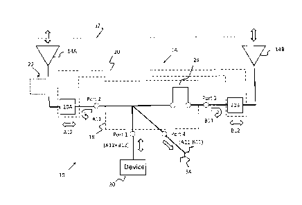
Referring to FIG. 1, an array antenna 10 is shown schematically. In the
exemplary embodiment, the array antenna 10 is a flat plate array antenna. The
array antenna 10 is intended for transmitting and/or receiving a plane wave
denoted by dashed line 12. The array antenna 10 includes a plurality of
radiating
antenna elements arranged to form an antenna aperture. The plurality of
radiating
antenna elements are arranged to include a first group of radiating antenna
elements 14A and a second group of radiating antenna elements 14B, similar in
properties but distinct in grouping, from the first group of radiating antenna
elements 14A. In the exemplary embodiment, the first group of radiating
antenna
elements 14A and second group of radiating antenna elements 14B each
represent one half of the radiating antenna elements defining the aperture of
the
array antenna 10.
The radiating antenna elements may be made up of any suitable known
type of array elements such as individual horns in a horn array, slots in a
slot
array, dipoles in a dipole array, patches in a patch array, etc., as well as
any
combination thereof. The array antenna 10 may represent an entire antenna, one
of several identical elements making up a larger array, a feed for another
antenna
system, etc., without departing from the scope of the invention.
The array antenna 10 further includes a corporate feed network 16
configured to feed the plurality of radiating antenna elements 14. The
corporate
feed network 16 includes as an input to the array antenna a 4-port device 18
such
as a magic T coupler, quadrature hybrid coupler, quadratUre hybrid ring
coupler or
other such suitable 4-port device. The 4-port device 18 includes a sum port
(Port
1), a difference port (Port 4), a first signal port (Port 2) and a second
signal port
=
(Port 3). The first signal port (Port 2) is coupled via the corporate feed
network to
the first group of radiating elements and the second signal port (Port 3) is
coupled
via the corporate feed network to the second group of radiating elements.
A "4-port device" as defined herein refers to any passive 4-port microwave
combining device whose microwave (network scattering) properties provide for
vector resolution of two independent (signal) ports into two orthogonal vector
components via the remaining two (output/input) ports. Orthogonality of the
two
5
CA 02887073 2015-04-02
THINP0109CA
vector-resolved channels may be in the form of amplitude pairs ("A+B" and "A-
B")
or alternatively in the form of complex-conjugate pairs ("A+jB" and "B+jA",)
depending on the specifics of the particular 4-port device. In the case of the
former (amplitude-only) device class, a 90 degree phase-shift (via
introduction of a
discrete phase-shifter or offset line-length) is added to one of the two
signal ports
in order to provide the requisite one-way 90 degree phase differential, while
this
supplemental section is unnecessary when employing a device in the latter
(complex-conjugate) class.
The corporate feed network 16 may include a corporate feed structure 20 in
addition to the 4-port device 18, the corporate feed structure 20 including
any of a
variety of conventional corporate feed devices such as couplers, splitters,
etc. As
described herein, the corporate feed structure 20 may be divided into a first
portion 20A and a second portion 20B for feeding the first and second groups
of
radiating antenna elements 14A, 14B, respectively. The corporate feed
structure
20 together with the 4-port device 18 may be constructed using any
conventional
transmission line approach, including waveguide, microstrip, stripline or
other, as
will be appreciated.
The array antenna 10 further includes a first phase shift element 22
proximal to the antenna aperture to introduce a first predetermined phase
shift, via
mechanical and/or dielectric means, to the first group of radiating antenna
elements 14A. Additionally, the array antenna 10 includes a second phase shift
element 24 proximal to the 4-port microwave device 18, at the second signal
port
(Port 3) to introduce a second predetermined phase shift to the second group
of
radiating antenna elements 14B.
The first phase shift element 22 may include a flat plate dielectric material
placed in front of the first group of radiating antenna elements 14A. For
example,
the flat plate dielectric material may include air and/or glass as discussed
below
with respect to FIGS. 2 and 3, respectively. As another example, the first
phase
shift element 22 may include a phase-shift line length coupled between the
first
group of radiating antenna elements 14A and the corporate feed network 16. The
line length may be made up of waveguide, microstrip, stripline, etc., as will
be
6
CA 02887073 2015-04-02
THINP0109CA
appreciated. The first phase shift element 22 preferably is configured to
introduce
an approximately 90 degree phase shift at mid frequency of an operating band
of
the array antenna. As referred to herein, "approximately 90 degrees" refers to
a
phase shift within the range of 90 degrees, plus or minus 20 degrees.
In an embodiment in which the 4-port device includes a magic T coupler,
the first signal port (Port 2) and the second signal port (Port 3) represent
respective ends of first and second collinear arms included in the magic T
coupler.
The second phase shift element 24 is an additional line length in the second
collinear arm added to compensate for the phase balance introduced by the
first
phase shift element 14A.
In an embodiment where the first phase shift element 22 is approximately
90 degrees, the second phase shift element 24 is approximately 90 degrees in
length with respect to a mid frequency of an operating band of the array
antenna
10. The second phase shift element 24 may be made up of waveguide,
microstrip, stripline, etc., as will be appreciated.
The 4-port device 18 may be any of various known types of 4-port devices
including, for example, a magic T coupler, a quadrature hybrid coupler, and/or
a
quadrature hybrid ring coupler.
Continuing to refer to FIG. 1, a device 30 such as a transmitter has its
output connected to the sum port (Port 1) of the 4-port device 18. The device
30
outputs a signal (Al2+612) into Port 1. One half of the signal (Al2) is
directed
towards the first group of radiating antenna elements 14A via Port 2 and the
first
portion 20A of the corporate feed structure 20. The other half of the signal
(B12)
is directed towards the second group of radiating antenna elements 146 via
Port 3
and the second portion 206 of the corporate feed structure 20. Undesired
reflections at Port 2 (All) are reflected back into Port 2 and are directed
within the
4-port device 18 to the difference port (Port 4) which is terminated with a
load 34
designed to absorb the reflections. Similarly, undesired reflections at Port 3
(611)
are reflected back into Port 3 and are directed within the 4-port device 18 to
the
difference port (Port 4) and into the load 34.
7
CA 02887073 2015-04-02
THINP0109CA
It will be appreciated that the device 30 could be connected to the
difference port (Port 4) and the load 34 connected to the sum port (Port 1)
and
similar operation occurs.
Thus, the array antenna 10 enjoys a substantial improvement in VSWR by
channeling the reflection caused by tolerance variation and/or inadequate
components' bandwidth to the "loaded" sum or difference ports of the magic T,
quadrature coupler or other 4-port device, while the difference or the sum
port
used for the signal input, respectively. Degradation in the input reflection
or the
radiation pattern is avoided since the phase change in half of the aperture is
corrected by the introduction of the second phase shift element 24 while the
undesired reflection is channeled into the loaded arm of the 4-way power
divider
isolated from main input. The array antenna 10 thus presents the simplicity of
using a piece of flat plate dielectric plus simple phase adjustment (e.g., in
the
collinear arms of a magic T) to achieve broader bandwidth without complicated
matching circuitry at the input.
In exemplary embodiments, a half aperture sized flat plate dielectric
material serving as the first phase shift element 22 is placed in front of the
first
group of radiating antenna elements 14A representing one half of the antenna
aperture. At the same time, the 4-port device 18 feeding the entire aperture
includes a purposeful phase shift in the form of the second phase shift
element 24
to compensate for the phase imbalance in the aperture introduced by the first
phase shift element 22. This intentional phase shift at the aperture and the 4-
port
device provides desired VSWR cancellation properties.
The half aperture sized flat plate dielectric material serving as the first
phase shift element 22 should be a half wavelength (wavelength inside the
dielectric medium) thick around the mid frequency of the operating band of the
array antenna 10. Ideally, glass material with the dielectric constant of 4
can
provide the thickness which is exactly the quarter of wavelength in free space
and
translates to a 90 degrees phase shift in free space. However, in the absence
of
the glass other dielectric materials, with appropriate thicknesses, can also
be used
to achieve similar improvement, while departing from a rigorous half-
wavelength
8
CA 02887073 2015-04-02
THINP0109CA
thickness criteria. Alternatively, multi-layer embodiments may be employed as
the
phase-shift element 22, in order to simultaneously provide both the desired
insertion phase correction and desired input match properties.
Referring to Figs. 2A-2B, shown is a first particular embodiment of the
present invention as described herein. The first group of radiating antenna
elements 14A is made up of four radiating antenna elements 14 coupled to Port
2
of the 4-port device 18 via a 1-to-4 power divider corporate feed structure
20A.
Similarly, the second group of radiating antenna elements 14B is made up of
four
radiating antenna elements 14 coupled to Port 3 of the 4-port device 18 via a
1-to-
4 power divider corporate feed structure 20B.
The 4-port device 18 in this embodiment is a 4-port waveguide magic-T.
Moreover, in this embodiment the first phase shift element 22 is made up of a
recessed half aperture. In this manner, the first phase shift element is an
air
dielectric 22a and is configured to introduce an approximately 90 degree phase
shift at mid frequency of an operating band of the array antenna. To offset
the
radiated phase impact due to the introduction of the air dielectric 22a, the 4-
port
device 18 includes phase imbalanced collinear arms. Specifically, the
collinear
arm at Port 3 includes an additional 90 degree feed-line length representing
the
second phase shift element 24.
Figs. 3A and 3B illustrate another particular embodiment similar to the
embodiment of Figs. 2A-2B but with the following exceptions. Rather than the
air
dielectric 22a, dielectric plate 22b is introduced at the antenna aperture in
front of
the radiating antenna elements 14A. To offset the radiated phase impact due to
the introduction of the dielectric plate 22b, the 4-port device 18 again
includes
phase imbalanced collinear arms. Specifically, the collinear arm at Port 3
includes
an additional 90 degree feed-line length representing the second phase shift
element 24.
Although the invention has been shown and described with respect to a
certain embodiment or embodiments, equivalent alterations and modifications
may occur to others skilled in the art upon the reading and understanding of
this
specification and the annexed drawings. In particular regard to the various
9
CA 02887073 2015-04-02
THINP01 09CA
functions performed by the above described elements (components, assemblies,
devices, compositions, etc.), the terms (including a reference to a "means")
used
to describe such elements are intended to correspond, unless otherwise
indicated,
to any element which performs the specified function of the described element
(i.e., that is functionally equivalent), even though not structurally
equivalent to the
disclosed structure which performs the function in the herein exemplary
embodiment or embodiments of the invention. In addition, while a particular
feature of the invention may have been described above with respect to only
one
or more of several embodiments, such feature may be combined with one or more
other features of the other embodiments, as may be desired and advantageous
for any given or particular application.