Note: Descriptions are shown in the official language in which they were submitted.
A DEVICE, SYSTEM AND METHOD FOR CHARGING A BATTERY
CROSS-REFERENCE TO RELATED APPLICATION
100011 This application claims priority from U.S. Patent Application No.
14/248,498, filed
April 9, 2014.
FIELD
100021 The specification relates generally to charging batteries, and
specifically to a
device, system and method for charging a battery.
BACKGROUND
100031 The Universal Serial Bus (USB) has evolved from a data interface
capable of
supplying limited power to a primary provider of power with a data interface.
Today
many devices charge or get their power from USB ports contained in laptops,
cars,
aircraft or even wall sockets. USB has become a ubiquitous power socket for
many small
devices such as cell phones, MP3 players and other hand-held devices. The
charger path
of USB systems currently includes a buck regulator inside the charger and then
again
another series of switching regulators and/or buck regulators in a device
being charged, to
provide constant current and voltage for charging a battery, for example, a
lithium
battery. Each one of these regulators add inefficiencies to the charging path.
The power
lost from switching (e.g. stepping up or down to a charging current and/or
voltage)
becomes heat and hence a power management integrated circuit (PMIC) must be
larger to
compensate for heat dissipation. The combination of increased footprint and
excess heat
reduce overall performance.
100041 While designs using two buck regulators (e.g. one in the charger and
one in the
device) can offer efficiencies of around 75%, they do not deliver optimal
amounts of
power to the battery to charge at maximal rates. A common strategy to combat
this is to
have VBUS output (of a USB port) at a higher voltage, at the same current
output, which
allows for higher power delivery to the system. However, this strategy creates
a few
challenges. For one, the system needs to have two buck regulators: a first one
to make the
inputs to system voltage regulators (e.g. LDOs (low dropout output regulators)
and the
like); and a second one to create a constant current constant voltage source
for the
1
Date Recue/Date Received 2021-09-28
CA 02887739 2015-04-08
battery. This also increased cost of the power path. Secondly, having to step
down from
an even higher voltage exasperates the heat dissipation problems.
BRIEF DESCRIPTIONS OF THE DRAWINGS
[0005] For a better understanding of the various implementations described
herein and to
show more clearly how they may be carried into effect, reference will now be
made, by
way of example only, to the accompanying drawings in which:
[0006] Fig. 1 depicts a schematic diagram of a system for charging a battery,
according
to non-limiting implementations.
[0007] Fig. 2 depicts a block diagram of a flowchart of a method for charging
a battery,
according to non-limiting implementations.
[0008] Fig. 3 depicts a device of the system of Fig. 1 transmitting a power
control signal
to a charger, and the charger delivering power to the device in accordance
with the power
control signal, according to non-limiting implementations.
[0009] Fig. 4 depicts the device of the system of Fig. 1 further regulating
power from the
charger in a feedback loop there between, according to non-limiting
implementations.
[0010] Fig. 5 depicts circuitry of the device of Fig. 1, according to non-
limiting
implementations.
[0011] Fig. 6 depicts circuitry of the charger of Fig. 1, according to non-
limiting
implementations.
DETAILED DESCRIPTION
[0012] The present disclosure describes examples of a system comprising a
charger and a
device, where the device calculates a target power and/or target voltage
and/or target
current to be output by the charger to the device along a power path for
charging a battery
at the device. The device outputs a power control signal to the charger via a
connection
with charger, the connection including, but not limited to, one or more of a
hardware
port, data port, an interface, hardware interface, a USB port, and the like.
The power
control signal is encoded with one or more of the target power and/or the
target voltage
and/or the target current. The charger receives the power control signal, the
charger
comprising respective circuitry for responding to the power control signal by
outputting
2
CA 02887739 2015-04-08
one or more of a power, a current and/or a voltage according to the encoding
in the power
control signal. This eliminates need for a stepping regulator in the device,
as the power
control signal causes the charger to output the target power/current/voltage,
rather than
the stepping regulator regulating to same; hence, the overall efficiency of
the power path
is increased due to the elimination of the need for the stepping regulator of
the device.
[0013] In this specification, elements may be described as "configured to"
perform one
or more functions or "configured for" such functions. In general, an element
that is
configured to perform or configured for performing a function is enabled to
perform the
function, or is suitable for performing the function, or is adapted to perform
the function,
or is operable to perform the function, or is otherwise capable of performing
the function.
[0014] Furthermore, as will become apparent, in this specification certain
elements may
be described as connected physically, electronically, or any combination
thereof,
according to context. In general, components that are electrically connected
are
configured to communicate (that is, they are capable of communicating) by way
of
electric signals. According to context, two components that are physically
coupled and/or
physically connected may behave as a single element. In some cases, physically
connected elements may be integrally formed, e.g., part of a single-piece
article that may
share structures and materials. In other cases, physically connected elements
may
comprise discrete components that may be fastened together in any fashion.
Physical
connections may also include a combination of discrete components fastened
together,
and components fashioned as a single piece.
[0015] In this specification reference is made to the term "port"; while the
term "port" in
the computer technical arts, can refer to a software port, it is explicitly
appreciated that
the term "port" as used in this specification refers to a hardware port, an
interface, a
hardware interface, a computer interface, and the like. Further the terms
"hardware port",
"interface" and/or "hardware interface" and/or "computer interface" can be
interchangeably used throughout this specification in place of the term
"port".
[0016] An aspect of the specification provides device comprising: a USB
(Universal
Serial Bus) port; a battery in communication with the USB port; and, circuitry
in
communication with the USB port and the battery, the circuitry configured to:
transmit a
power control signal over the USB port, the power control signal comprising
data
3
CA 02887739 2015-04-08
4
indicative of one or more of a power, a voltage and a current to be received
over the USB
port to charge the battery; and, responsively receive the power for charging
the battery
over the USB port.
[0017] The power control signal can comprise a pulsed width modulation (PWM)
signal
transmitted over a USB Identification (USBID) connector of the USB port, and
the power
is responsibly received over a Voltage Bus (VBUS) connector of the USB port.
[0018] The power control signal can comprise an analog signal transmitted over
a VBUS
connector of the USB port, and the power is responsibly received over the VBUS
connector.
[0019] The power control signal can comprise a digital signal transmitted over
one or
more of a USB D+ connector and a USB D- connectors of the USB port, and the
power is
responsibly received over a VBUS connector of the USB port.
[0020] The power control signal can comprise one or more of a PWM signal, an
analog
signal and a digital signal transmitted over one or more of a USBID connector,
a VBUS
connector, a USB D+ connector, and a USB D- connector, of the USB port, and
the
power is responsibly received over the VBUS connector.
[0021] The circuitry can be configured to: determine a target current to be
received at the
USB port for charging the battery; and adjust the power control signal so that
the target
current is received at the USB port.
[0022] The circuitry can be configured to: determine a target voltage to be
received at the
USB port for charging the battery, and adjust the power control signal so that
the target
voltage is received at the USB port.
[0023] The circuitry can comprise a power management integrated circuit (PMIC)
in line
between the USB port and the battery, the PMIC configured to: determine one or
more of
a received voltage and a received current from the USB port; and the circuitry
further
configured to: adjust the power control signal based on one or more of the
received
voltage and the received current so that one or more of: the received current
approaches a
target current; and the received voltage approaches a target voltage.
[0024] Another aspect of the specification provides a method comprising: at a
device
comprising: a USB (Universal Serial Bus) port; a battery in communication with
the USB
port; and, circuitry in communication with the USB port and the battery,
transmitting,
4
CA 02887739 2015-04-08
using the circuitry, a power control signal over the USB port, the power
control signal
comprising data indicative of one or more of a power, a voltage and a current
to be
received over the USB port to charge the battery; and, responsively receiving,
at the
circuitry, the power for charging the battery over the USB port.
[0025] The power control signal can comprise a pulsed width modulation (PWM)
signal
transmitted over a USB Identification (USBID) connector of the USB port, and
the power
is responsibly received over a Voltage Bus (VBUS) connector of the USB port.
[0026] The power control signal can comprise an analog signal transmitted over
a VBUS
connector of the USB port, and the power is responsibly received over the VBUS
connector.
[0027] The power control signal can comprise a digital signal transmitted over
one or
more of a USB D+ connector and a USB D- connectors of the USB port, and the
power is
responsibly received over a VBUS connector of the USB port.
[0028] The power control signal can comprise one or more of a PWM signal, an
analog
signal and a digital signal transmitted over one or more of a USBID connector,
a VBUS
connector, a USB D+ connector, and a USB D- connector, of the USB port, and
the
power is responsibly received over the VBUS connector.
[0029] The method can further comprise: determining, at the circuitry, a
target current to
be received at the USB port for charging the battery; and adjusting the power
control
signal so that the target current is received at the USB port.
[0030] The method can further comprise: determining, at the circuitry, a
target voltage to
be received at the USB port for charging the battery; and adjusting, at the
circuitry, the
power control signal so that the target voltage is received at the USB port.
[0031] The circuitry can comprise a power management integrated circuit (PMIC)
in line
between the USB port and the battery, the PMIC configured to: determine one or
more of
a received voltage and a received current from the USB port; and the circuitry
configured
to: adjust the power control signal based on one or more of the received
voltage and the
received current so that one or more of: the received current approaches a
target current;
and the received voltage approaches a target voltage.
[0032] Yet a further aspect of the specification provides a computer program
product,
comprising a computer usable medium having a computer readable program code
CA 02887739 2015-04-08
adapted to be executed to implement a method comprising: at a device
comprising: a
USB (Universal Serial Bus) port; a battery in communication with the USB port;
and,
circuitry in communication with the USB port and the battery, transmitting,
using the
circuitry, a power control signal over the USB port, the power control signal
comprising
data indicative of one or more of a power, a voltage and a current to be
received over the
USB port to charge the battery; and, responsively receiving, at the circuitry,
the power for
charging the battery over the USB port. The computer usable medium can
comprises a
non-transitory computer usable medium. The method can further comprise;
determining,
at the circuitry, a target current to be received at the USB port for charging
the battery;
and adjusting the power control signal so that the target current is received
at the USB
port. The method can further comprise: determining, at the circuitry, a target
voltage to
be received at the USB port for charging the battery; and adjusting, at the
circuitry, the
power control signal so that the target voltage is received at the USB port.
100331 Yet a further aspect of the specification provides a system comprising:
a charger
comprising: a respective USB (Universal Serial Bus) port; and respective
circuitry
configured to receive a power control signal over the respective USB port;
and,
responsively transmit power over the respective USB port according to data in
the power
control signal; and, a device comprising: a USB port configured to communicate
with the
respective USB port of the charger; a battery in communication with the USB
port; and,
circuitry in communication with the USB port and the battery, the circuitry
configured to:
transmit the power control signal over the USB port to the charger, the data
in the power
control signal comprising data indicative of one or more of a power, a voltage
and a
current to be received over the USB port to charge the battery; and,
responsively receive
the power for charging the battery over the USB port.
100341 Yet a further aspect of the specification provides device comprising: a
hardware
port; a battery in communication with the hardware port; and, circuitry in
communication
with the hardware port and the battery, the circuitry configured to: transmit
a power
control signal over the hardware port, the power control signal comprising
data indicative
of one or more of a power, a voltage and a current to be received over the
hardware port
to charge the battery; and, responsively receive the power for charging the
battery over
the hardware port.
6
CA 02887739 2015-04-08
[0035] The power control signal can comprise a pulsed width modulation (PWM)
signal
transmitted over one or more of an identification connector and a data
connector of the
hardware port, and the power is responsibly received over a voltage connector
of the
hardware port.
[0036] The power control signal can comprise an analog signal transmitted over
a voltage
connector of the hardware port, and the power is responsibly received over the
voltage
connector.
[0037] The power control signal can comprise a digital signal transmitted over
one or
more data connectors of the hardware port, and the power is responsibly
received over a
voltage connector of the hardware port.
100381 The power control signal can comprise one or more of a PWM signal, an
analog
signal and a digital signal transmitted over one or more of an identification
connector, a
voltage connector, and a data connector of the hardware port, and the power is
responsibly received over the voltage connector.
[0039] The circuitry can be configured to: determine a target current to be
received at the
hardware port for charging the battery; and adjust the power control signal so
that the
target current is received at the hardware port.
[0040] The circuitry can be configured to: determine a target voltage to be
received at the
hardware port for charging the battery, and adjust the power control signal so
that the
target voltage is received at the hardware port.
[0041] The circuitry can comprise a power management integrated circuit (PMIC)
in line
between the hardware port and the battery, the PMIC configured to: determine
one or
more of a received voltage and a received current from the hardware port; and
the
circuitry further configured to: adjust the power control signal based on one
or more of
the received voltage and the received current so that one or more of: the
received current
approaches a target current; and the received voltage approaches a target
voltage.
[0042] Another aspect of the specification provides a method comprising: at a
device
comprising: a hardware port; a battery in communication with the hardware
port; and,
circuitry in communication with the hardware port and the battery,
transmitting, using the
circuitry, a power control signal over the hardware port, the power control
signal
comprising data indicative of one or more of a power, a voltage and a current
to be
7
CA 02887739 2015-04-08
received over the hardware port to charge the battery; and, responsively
receiving, at the
circuitry, the power for charging the battery over the hardware port.
[0043] The power control signal can comprise a pulsed width modulation (PWM)
signal
transmitted over one or more of an identification connector and a data
connector of the
hardware port, and the power is responsibly received over a voltage connector
of the
hardware port.
[0044] The power control signal can comprise an analog signal transmitted over
a voltage
connector of the hardware port, and the power is responsibly received over the
voltage
connector.
[0045] The power control signal can comprise a digital signal transmitted over
one or
more a data connector of the hardware port, and the power is responsibly
received over a
voltage connector of the hardware port.
[0046] The power control signal can comprise one or more of a PWM signal, an
analog
signal and a digital signal transmitted over one or more of an identification
connector, a
voltage connector, and a data connector, of the hardware port, and the power
is
responsibly received over the voltage connector.
[0047] The method can further comprise: determining, at the circuitry, a
target current to
be received at the hardware port for charging the battery; and adjusting the
power control
signal so that the target current is received at the hardware port.
[0048] The method can further comprise: determining, at the circuitry, a
target voltage to
be received at the hardware port for charging the battery; and adjusting, at
the circuitry,
the power control signal so that the target voltage is received at the
hardware port.
[0049] The circuitry can comprise a power management integrated circuit (PMIC)
in line
between the hardware port and the battery, the PMIC configured to: determine
one or
more of a received voltage and a received current from the hardware port; and
the
circuitry configured to: adjust the power control signal based on one or more
of the
received voltage and the received current so that one or more of: the received
current
approaches a target current; and the received voltage approaches a target
voltage.
[0050] Yet a further aspect of the specification provides a computer program
product,
comprising a computer usable medium having a computer readable program code
adapted to be executed to implement a method comprising: at a device
comprising: a
8
CA 02887739 2015-04-08
hardware port; a battery in communication with the hardware port; and,
circuitry in
communication with the hardware port and the battery, transmitting, using the
circuitry, a
power control signal over the hardware port, the power control signal
comprising data
indicative of one or more of a power, a voltage and a current to be received
over the
hardware port to charge the battery; and, responsively receiving, at the
circuitry, the
power for charging the battery over the hardware port. The computer usable
medium can
comprises a non-transitory computer usable medium. The method can further
comprise:
determining, at the circuitry, a target current to be received at the hardware
port for
charging the battery; and adjusting the power control signal so that the
target current is
received at the hardware port. The method can further comprise: determining,
at the
circuitry, a target voltage to be received at the hardware port for charging
the battery; and
adjusting, at the circuitry, the power control signal so that the target
voltage is received at
the hardware port.
[0051] Yet a further aspect of the specification provides a system comprising:
a charger
comprising: a respective hardware port; and respective circuitry configured to
receive a
power control signal over the respective hardware port; and, responsively
transmit power
over the respective hardware port according to data in the power control
signal; and, a
device comprising: a hardware port configured to communicate with the
respective
hardware port of the charger; a battery in communication with the hardware
port; and,
circuitry in communication with the hardware port and the battery, the
circuitry
configured to: transmit the power control signal over the hardware port to the
charger, the
data in the power control signal comprising data indicative of one or more of
a power, a
voltage and a current to be received over the hardware port to charge the
battery; and,
responsively receive the power for charging the battery over the hardware
port.
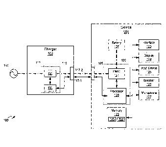
[0052] Fig. 1 depicts a system 100 comprising a device 101 and a charger 103,
according
to non-limiting implementations. Device 101 comprises: a port 105; a battery
107 in
communication with port 105; and, circuitry 109 in communication with port 105
and
battery 107, circuitry 109 configured to: transmit a power control signal over
port 105,
the power control signal comprising data indicative of one or more of a power,
a voltage
and a current to be received over port 105 to charge battery 107; and,
responsively
receive the power for charging battery 107 over port 105. Charger 103
comprises: a
9
CA 02887739 2015-04-08
respective port 115 (in communication with port 105 via one or more links 117-
1, 117-2,
for example); and respective circuitry 113 configured to receive the power
control signal
over respective port 115; and, responsively transmit power over respective
port 115
according to the data in the power control signal.
[0053] Circuitry 109 can generally comprise: a processor 120 in communication
with a
power management integrated circuitry (PMIC) 121; in some implementations,
processor
120 and PMIC 121 can be combined, while in other implementations, as depicted,
processor 120 and PMIC 121 can be separate devices.
[0054] Device 101 further comprises: a memory 122, and optionally, a
communication
interface 123 (interchangeably referred to hereafter as interface 123), a
display 124, an
input device 125, a speaker 126 and a microphone 127.
[0055] Circuitry 113 generally comprises a controller 130 in communication
with a
power regulator 131 (interchangeably referred to hereafter as regulator 131);
in some
implementations, controller 130 and regulator 131 can be combined, while in
other
implementations, as depicted, controller 130 and regulator 131 can be separate
devices.
[0056] Charger 103, and specifically regulator 131, can be further connected
to an
external power supply 140, for example a mains power supply 140, and the like,
outputting alternating current.
[0057] Each of circuitry 109, 113 are depicted in stippled lines surrounding
respective
components of each of device 101 and charger 103 including, but not limited
to,
respectively, processor 120 and PMIC 121, and controller 130 and regulator
131. Other
components (not depicted) can be part of each of circuitry 109, 113, as
described below.
However, circuitry 109 is specifically lacking a regulator between PMIC 121
and battery
107.
[0058] Furthermore, in Fig. 1, data paths and/or data links are depicted as
solid lines,
while power paths and/or power links are depicted as broken lines
(specifically, dash-
dash-dot, for example link 117-2).
[0059] Ports 105, 115 are each configured to communicate with each other, for
example,
when linked via one or more links 117-1, 117-2, interchangeably referred to
hereafter,
collectively, as links 117 and generically as a link 117.
CA 02887739 2015-04-08
[0060] Each port 105, 115 can comprise one or more of a hardware port, data
port, an
interface, a hardware interface, a USB (universal serial bus) port and the
like.
[0061] Furthermore, while specific implementations are described with respect
to ports
105, 115 being USB ports, ports 105, 115 can include any suitable hardware
port where a
power control signal can be transmitted from port 105 to port 115 via a link
there
between, and power is responsibly received at port 105 from port 115 via a
link there
between. Such hardware ports can include, but are not limited to, ethernet
ports, parallel
ports, serial ports, IEEE 1394 ports, PS/2 ports, VGA (Video Graphics Array)
ports, DVI
(Digital Visual Interface) ports, SCSI (Small Computer System Interface)
ports, HDMI
(High-Definition Multimedia Interface) ports, and the like.
[0062] Furthermore, current implementations can be applied to any USB
specification,
including, but not limited to USB specifications 3.1, 3.0, 2.0, 1.0,
including, but not
limited to, USB specification 3.1 released on July 26, 2013, as well as any
future USB
specifications, and/or updates to current USB specifications. Current
implementations
can further be applied to any USB specification that is not defined by
"official" USB
specifications, for example proprietary USB specifications and/or modified USB
specifications (e.g. USB specifications which can be based on one or more of
USB
specifications 3.1, 3.0, 2.0, 1.0, and/or future "official" USB
specifications, but do not
strictly adhere to such) and/or variations of USB specifications.
[0063] Links 117 can comprise a suitable combination of cables and connectors
to link
ports 105, 115 to each other. For example, when each of ports 105, 115
comprise a USB
port, links 117 can comprise a USB cable connected to each of ports 105, 115.
Hence,
links 117 can be removable from each of device 101 and charger 103, and/or
links 117
can be removabley connected to each of ports 105, 115.
100641 While links 117 are depicted as separate in Fig. 1, links 117 can be
combined in a
single cable, either as separate lines in the single cable or the same line in
the single
cable.
100651 In general, links 117 can convey data signals between device 101 and
charger
103, including but not limited to power control signals, and further convey
power from
charger 103 to device 101 to charge battery 107. For example, as depicted,
processor 120
can transmit a power control signal to controller 130 via link 117-1, and
controller 130
11
CA 02887739 2015-04-08
can responsively control regulator 131 to provide power from power supply 140
to PMIC
121 via link 117-2, which in turn conveys the power to battery 107 to charge
battery 107.
[0066] It should be emphasized that the structure of device 101 in Fig. 1 is
purely an
example, and contemplates a device that can be used for both wireless voice
(e.g.
telephony) and wireless data communications (e.g. email, web browsing, text,
and the
like). However, Fig. I contemplates a device that can be used for any suitable
specialized
functions, including, but not limited, to one or more of, telephony,
computing, appliance,
and/or entertainment related functions.
[0067] Device 101 comprises at least one input device 125 generally configured
to
receive input data, and can comprise any suitable combination of input
devices, including
but not limited to a keyboard, a keypad, a pointing device, a mouse, a track
wheel, a
trackball, a touchpad, a touch screen and the like. Other suitable input
devices are within
the scope of present implementations.
[0068] Input from input device 125 is received at processor 120 (which can be
implemented as a plurality of processors, including but not limited to one or
more central
processors (CPUs)). Processor 120 is configured to communicate with a memory
122
comprising a non-volatile storage unit (e.g. Erasable Electronic Programmable
Read Only
Memory ("EEPROM"), Flash Memory) and a volatile storage unit (e.g. random
access
memory ("RAM")). Programming instructions that implement the functional
teachings
of device 101 as described herein are typically maintained, persistently, in
memory 122
and used by processor 120 which makes appropriate utilization of volatile
storage during
the execution of such programming instructions. Those skilled in the art will
now
recognize that memory 122 is an example of computer readable media that can
store
programming instructions executable on processor 120. Furthermore, memory 122
is also
an example of a memory unit and/or memory module.
[0069] Memory 122 further stores an application 145 that, when processed by
processor
120, enables processor 120 to: transmit a power control signal over port 105,
for example
via link 117-1, the power control signal comprising data indicative of one or
more of a
power, a voltage and a current to be received over port 105 to charge battery
107 so that
PMIC 121 can responsively receive the power for charging battery 107 over port
105, for
example via link 117-2.
12
CA 02887739 2015-04-08
[0070] Furthermore, memory 122 storing application 145 is an example of a
computer
program product, comprising a non-transitory computer usable medium having a
computer readable program code adapted to be executed to implement a method,
for
example a method stored in application 145.
[0071] Memory 122 can further store data 150 indicative of target charging
conditions
for battery 107, including, but not limited to, one or more of a target charge
current, a
target charge voltage, a target charge power, and the like. Data 150 can
further (and
optionally) comprise include a plurality of target charging conditions for
battery 107; for
example, in some implementations, circuitry 109 can include a fuel gauge (not
depicted)
configured to determine a degree of charging of battery 107 and/or a charge
state of
battery 107, and target charging conditions can change based on a degree to
which
battery 107 is charged and/or a charge state of battery 107, as measured by
the fuel gauge
(e.g. a target charging current can be different when the battery is drained
than when the
battery is 90% charged).
[0072] Data 150 can further (and optionally) comprise target charging
conditions for a
plurality of batteries; for example, each battery and/or battery type that can
be inserted
into device 101 can have different charging specifications; hence, if battery
107 is of a
given type, and is replaced by another battery of a different type (e.g. of
battery 107 and a
replacement battery have different product numbers and/or are based on
different
technologies and/or different materials and/or different chemicals), the
target charge
current can change. Hence data 150 can comprise target charging conditions
and/or a
plurality of target conditions for a plurality of batteries and/or battery
types.
[0073] PMIC 121 generally comprises integrated circuits, and the like, for
managing
power requirements of device 101. In general, PMIC 121 can comprise switches,
FETs
(field-effect transistors) and the like for controlling power to charge
battery 107; PMIC
121 can further comprise one or more LDOs (low drop-out regulator).
[0074] PMIC 121 can optionally be configured to determine one or more of an
input
voltage, an output voltage and a current passing there through, and
communicate one or
more of the input voltage, the output voltage and the current passing there
through to
processor 120. Hence, PMIC 121 can optionally comprise one or more sensors for
13
CA 02887739 2015-04-08
sensing one or more of: current passing there through, an input voltage, an
output
voltage, a voltage across PMIC 121, and the like.
[0075] Hence, PMIC 121 can determine a charging current passing there through
and/or
a voltage drop there across (e.g. input voltage minus output voltage) and
convey data
indicating such to processor 120; processor 120 can compare the charging
current and/or
voltage drop at PMIC 121 and compare to target charging conditions for battery
107 as
stored in data 150. Processor 120 can transmit a power control signal to
charger 103 via
ports 105, 115 and link 117-1 to adjust the charging conditions when existing
charging
conditions are different from the target charging conditions.
[0076] In other words, when device 101 is connected to charger 103 via ports
105, 115
and links 117, device 101 can initially transmit a power control signal to
charger 103 via
ports 105, 115, and link 117-1, the power control signal comprising target
charging
conditions as stored in data 150, thereby causing charger 103 to convey power
to PMIC
121 via ports 105, 115 and link 117-2; ideally, charger 103 delivers power to
PMIC 121
according to the target charging conditions, and PMIC 121 conveys the power to
battery
107 to charge battery 107. However, PMIC 121 can optionally monitor the actual
charging conditions (i.e. input voltage, output voltage and/or charging
current passing
there through) and convey same to processor 120, which can adjust the charging
conditions by transmitting one or more further charging conditions to charger
103. As
such device 101 and charger 103 form a feedback loop for charging battery 107,
in order
to attain the target charging conditions stored in data 150.
[0077] In some implementations, memory 122 and/or PMIC 121 and/or application
145
and/or data 150 can further store electrical characteristics of PMIC 121,
including, but
not limited to, a resistance of PMIC 121 so that processor 120 can convert a
voltage
across PMIC 121 to a current passing there through and/or convert a current
passing there
through to a voltage there across using, for example, Ohm's Law.
[0078] Processor 120 can be further configured to communicate with display
124, and
speaker 126, and microphone 127. Display 124 comprises any suitable one of, or
combination of, flat panel displays (e.g. LCD (liquid crystal display), plasma
displays,
OI,ED (organic light emitting diode) displays, capacitive or resistive
touchscrecns, CRTs
(cathode ray tubes) and the like). Speaker 126 comprises any suitable speaker
for
14
CA 02887739 2015-04-08
converting audio data to sound to provide one or more of audible alerts,
audible
communications from remote communication devices, and the like. Microphone 127
comprises any suitable microphone for receiving sound and converting to audio
data. In
some implementations, input device 125 and display 124 are external to device
101, with
processor 120 in communication with each of input device 125 and display 124
via a
suitable connection and/or link.
[0079] Processor 120 also connects to interface 123, which can be implemented
as one or
more radios and/or connectors and/or network adaptors and/or transceivers,
configured to
wirelessly communicate with one or more communication networks (not depicted),
for
example via antennas (not depicted). It will be appreciated that interface 123
is
configured to correspond with network architecture that is used to implement
one or more
communication links to the one or more communication networks, including but
not
limited to any suitable combination of USB (universal serial bus) cables,
serial cables,
wireless links, cell-phone links, cellular network links (including but not
limited to 26,
2.5G, 3G, 4G+ such as UMTS (Universal Mobile Telecommunications System), GSM
(Global System for Mobile Communications), CDMA (Code division multiple
access),
FDD (frequency division duplexing), LTE (Long Term Evolution), TDD (time
division
duplexing), TDD-LTE (TDD-Long Term Evolution), TD-SCDMA (Time Division
Synchronous Code Division Multiple Access) and the like, wireless data,
Bluetooth links,
NFC (near field communication) links, WLAN (wireless local area network)
links, WiFi
links, WiMax links, packet based links, the Internet, analog networks, the
PSTN (public
switched telephone network), access points, and the like, and/or a
combination.
Specifically, interface 123 comprises radio equipment (i.e. a radio
transmitter and/or
radio receiver) for receiving and transmitting signals, for example using
antennas (not
depicted).
[0080] Battery 107 comprises a rechargeable battery, including, but not
limited to, a
lithium battery, a nickel-cadmium battery, and the like. In some
implementations, battery
107 can be replaceable (e.g. device 101 can comprises a battery holder
accessible by a
user), while, in other implementations, battery 107 is not replaceable.
[0081] While not depicted, device 101 generally comprises one or more of a
chassis and
a housing for housing and/or supporting and/or containing components of device
101
CA 02887739 2015-04-08
and/or to further provide structural integrity to device 101. The chassis
and/or housing
can include, but is not limited to, an outer housing, an internal frame and
the like. The
chassis and/or housing can further comprise apertures for accessing components
of
device 101, for example an aperture to view display 124 and an aperture for
accessing
port 105.
[0082] In any event, it should be understood that a wide variety of
configurations for
device 101 are contemplated.
[0083] Charger 103 can comprise a battery charger and the like for charging
battery 107
at device 101 and batteries at other devices. Controller 130 can comprise one
or more of a
processor, a microeontroller and the like configured to: communicate with
circuitry 109
and/or processor 120 to receive a power control signal there from; and control
regulator
131 to provide power to one or more of circuitry 109, PMIC 121 and battery 107
to
charge battery 107, according to charging conditions received in the power
control signal
at controller 130. Regulator 131 comprises one or more of a variable
regulator, a variable
output regulator, a buck regulator, a switching regulator, and the like for
receiving input
power from power supply 140 and converting the input power from power supply
140 to
output power to one or more of circuitry 109, PMIC 121 and battery 107 to
charge
battery 107. In general, output power of regulator 131 is variable based on
signals from
controller 130, which in turn are based on a power control signal from device
101.
Furthermore, charger 103, circuitry 113, and/or regulator 131 can comprise an
AC
(alternating current) to DC (direct current) converter in the event that
charging is to occur
using direct current rather than alternating current as output by power supply
140.
[0084] While not depicted, charger 103 can further comprise a memory, for
example at
controller 130 storing an application that, when processed by controller 130,
causes
circuitry 113 to be configured to: receive a power control signal over port
115 (e.g. at
controller 130); and, responsively transmit power over port 115 according to
data in the
power control signal (e.g. controller 130 controls regulator 131 to vary
and/or change
power output from regulator 131 according to the power control signal).
Furthermore, a
memory at charger 103 storing such an application is an example of a computer
program
product, comprising a non-transitory computer usable medium having a computer
16
CA 02887739 2015-04-08
readable program code adapted to be executed to implement a method, for
example a
method stored in the application at charger 103.
[0085] Attention is next directed to Fig. 2 which depicts a flowchart
illustrating a method
200 of charging a battery, according to non-limiting implementations. In order
to assist in
the explanation of method 200, it will be assumed that method 200 is performed
using
system 100. Furthermore, the following discussion of method 200 will lead to a
further
understanding of system 100 and its various components. However, it is to be
understood
that system 100 and/or method 200 can be varied, and need not work exactly as
discussed
herein in conjunction with each other, and that such variations are within the
scope of
present implementations. It is appreciated that, in some implementations,
method 200 is
implemented in system 100 by processor 120 of device 101, for example by
implementing application 145.
[0086] It is to be emphasized, however, that method 200 need not be performed
in the
exact sequence as shown, unless otherwise indicated; and likewise various
blocks may be
performed in parallel rather than in sequence; hence the elements of method
200 are
referred to herein as "blocks" rather than "steps". It is also to be
understood that method
200 can be implemented on variations of system 100 as well.
[0087] At block 201, processor 120 detects charger 103; for example, when
charger 103
is connected to device 101 via ports 105, 115 and links 117, processor 120 and
controller
130 can exchange handshake signals and the like, the handshake signals
indicating to
each of processor 120 and charger 103 the presence of the other of processor
120 and
charger 103.
[0088] At block 203, processor 120 determines target charging conditions, for
example
by processing data 150; in some implementations, at block 203, processor 120
can further
and optionally) determine a battery type of battery 107; for example in some
implementations battery 107 comprises a memory (not depicted), and the like,
storing an
identifier thereof, and processor 120 can be configured to retrieve the
identifier from the
memory of battery 107, and in turn retrieve the charging conditions from data
150. Either
way, processor 120 can retrieve target charging conditions from data 150 at
memory 122.
[0089] In yet a further alternative, at block 203, processor 120 can determine
an existing
degree of charging and/or a charge state of battery 107, for example via the
above
17
CA 02887739 2015-04-08
described optional fuel gauge, and retrieve charging conditions from data 150
based
thereupon.
[0090] At block 205, processor 120 transmits a power control signal to charger
103, via
ports 105, 115, and link 117-1, the power control signal comprising target
charging
conditions for charging battery 107. Controller 130 receives the target
charging
conditions and controls regulator 131 to output power to port 115 according to
the target
charging conditions, for example a target charging current, target charging
voltage,
and/or target charging power. The power is received at port 105, and hence at
PMIC 121
and battery 107 to charge battery 107.
[0091] In some implementations, method 200 can end at block 205 and/or when
battery
107 is charged and/or when charger 103 and/or link 117 is disconnected from
device 101.
However, in other implementations, a feedback loop can occur between device
101 and
charger 103 as described hereafter with respect to blocks 207 to 211.
[0092] At block 207, processor 120 receives the existing charging conditions
from PMIC
121, including, but not limited to, the existing charging current and/or a
voltage across
PMIC 121 which can alternatively be converted to charging current using the
resistance
of PMIC 121 and Ohm's Law.
[0093] At block 209, processor 120 can compare the existing charging
conditions to the
target charging conditions; in some of these implementations, the target
charging
conditions can change based on a degree of charging and/or a charge state of
battery 107
as measured by the optional fuel gauge, described above. Either way, when the
existing
charging conditions are different from the target charging conditions (e.g. a
"Yes"
decision at block 209), at block 211, processor 120 can adjust the existing
charging
conditions by transmitting a further power control signal to charger 103.
Processor 120
continues to monitor the existing charging conditions at block 207. However,
when the
existing charging conditions are not different from the target charging
conditions (e.g. a
"No" decision at block 209), processor 120 continues to monitor the existing
charging
conditions at block 207. In general, blocks 207 to 211 repeat in a feedback
loop so that
the existing charging conditions converge on the target charging conditions
(e.g. a target
charging current through PMIC 121 and/or to battery 107, and/or a target
voltage across
PMIC 121, based on a target charging current and Ohm's Law).
18
CA 02887739 2015-04-08
[0094] In the feedback loop, in a specific non-limiting example, circuitry 109
is generally
configured to: determine a target current to be received over port 105 for
charging battery
107, and adjust power control signal 411 so that the target current is
received over port
105. Alternatively, circuitry 109 can be generally be configured to: determine
a target
voltage to be received over port 105 for charging battery 107, and adjust
power control
signal 411 so that the target voltage is received over port 105. Power control
signal 411
can comprise one or more absolute target charging conditions and/or an amount
of
current and/or voltage and/or power by which output of charger 103 is to be
changed (i.e.
an increase or a decrease in current and/or voltage and/or power).
[0095] As described above circuitry 109 comprises PMIC 121 in line between
port 105
and battery 107, PMIC 121 configured to: determine one or more of a received
voltage
and a received current from port 105; and circuitry 109 (e.g. processor 120)
further
configured to: adjust power control signal 411 based on one or more of the
received
voltage and the received current so that one or more of: the received current
approaches a
target current; and the received voltage approaches a target voltage.
[0096] It is appreciated that the existing charging conditions being the same
and/or
different from the target charging conditions need not comprise an exact match
and/or
and exact mismatch; in other words, the existing charging conditions can be
considered
the same as the target charging conditions as long as the existing charging
conditions are
within a given percentage of the target charging conditions, for example,
within 5%, 10%
and/or any percentage as chosen by an administrator and/or a designer of
system 100.
[0097] Method 200 will now be described with reference to Figs. 3 to 4, each
of which
are similar to Fig. 1, with like elements having like numbers.
[0098] At Fig. 3, processor 120 has detected charger 103 (e.g. via
handshaking) and
transmits a power control signal 301 to charger 103 via ports 105, 115 and
link 117-1
based on data 150, data 150 processed by processor 120. Controller 130
processes power
control signal 301 to determine target charging conditions and controls
charger 103 to
provide power 303 via ports 105, 115 and link 117-2, power 303 comprising
voltage
and/or current and/or power according to the target charging conditions in
power control
signal 301. In other words, Fig. 3 depicts blocks 201, 203 and 205 of method
200.
19
CA 02887739 2015-04-08
100991 At Fig. 4, processor 120 receives existing charging conditions 401 from
PMIC
121 and compares to the target charging conditions as stored in data 150. When
existing
charging conditions 401 are different from target charging conditions (for
example, when
voltage and/or current from regulator 131 drifts and/or controller 130
incorrectly
processed target power signal 301), processor 120 transmits a further power
control
signal 411 to charger 103, further power control signal 411 comprising data
for adjusting
power 303 towards the target charging conditions; for example, controller 130
responsively adjusts regulator 131 to provide adjusted power 413, power 413
adjusted
closer towards the target charging conditions. In other words, Fig. 4 depicts
blocks 207,
209 and 211 of method 200.
[00100] Power control signals 301, 411 can comprise one or more of a pulsed
width modulation (PWM) signal, an analog signal, a digital signal and the
like. For
example, attention is directed to Fig. 5 which depicts a specific non-limiting
example of
circuitry 109 and port 105, when port 105 comprises a USB port and a power
control
signal comprises a PWM signal. In these implementations, port 105 comprises
five USB
connectors: a VBus (voltage bus) connector for receiving power from charger
103; a
USBID (USB identifier) connector generally used for conveying USB identifier
signals
between devices; a D+ connector and a D- connector for conveying data signals
between
devices, and a ground connector, labelled GND in Fig. 5.
[00101] In any event, in depicted implementations processor 120 transmits a
power
control signal 501 over USBID connector, power control signal 501 comprising a
PWM
signal comprising, in a non-limiting example, a frequency that is 1000 times a
target
charging voltage to be output to PMIC 121 by charger 103 over the VBus
connector.
Power control signal 501 can comprise one or more of power control signals
301, 411.
[00102] Fig. 5 also depicts processor 120 being alternatively connected to
both the
D+ connector and D- connector, a wired link 503 between PMIC 121 and processor
120
for conveying existing operating conditions to processor 120. A zener diode
507 between
VBus connector and ground is also shown. While not depicted PMIC 121 can
further
comprise circuits for sending voltage and/or current at PMIC 121 and/or one or
more
switches and/or FETs for controlling power to battery 107.
CA 02887739 2015-04-08
1001031 While circuitry 109 can comprise further components, and/or
different
components, circuitry 109 is specifically lacking a regulator and/or a buck
regulator
between PMIC 121 and battery 107, which increases the efficiency of circuitry
109 as
compared to similar devices that include a regulator between a PMIC and a
battery..
1001041 Attention is next directed to Fig. 6, which depicts circuitry 113
at charger
103 which is compatible with circuitry 109 as depicted in Fig. 5, and when
port 115 also
comprises a USB port and the power control signal comprises a PWM signal. In
these
implementations, port 115 comprises five USB connectors: a VBus connector for
providing power to device 101; a USBID (USB identifier) connector generally
used for
conveying USB identifier signals between devices; a D+ connector and a D-
connector
for conveying data signals between devices, and a ground connector, labelled
GND in
Fig. 6. In other words, port 115 in Fig. 6 is substantially similar to port
105 in Fig. 5;
when ports 105, 115 are connected, for example using a USB cable and
connectors, each
connector at each port 105, 115 is connected to a corresponding connector at
the other
port 105, 115. For example, each VBus connector is connected to each other,
each D+
connector is connected to each other, each D- connector is connected to each
other, each
USBID connector is connected to each other and each GND connector is connected
to
each other.
1001051 Hence, in Fig. 6, controller 130 is connected to USBID connector of
port
115 so that power control signal 501, comprising the PWM signal, from USBID
connector of port 115 is received from processor 120 at device 101, when
device 101 and
charger 103 are connected. Controller 130 is connected to USBID connector via
an
optional sub-circuit 601 configured to modulate power control signal 501 for
controller
130; in other implementations, sub-circuit 601 is absent from circuitry 109
and/or
integrated into controller 130. Regardless, controller 130 is configured to
receive power
control signal 501 and control regulator 131 accordingly to output power to
device 101.
For example, when power control signal 501 comprises a signal that is a
frequency that is
1000 times a target charging voltage to be output to PMIC 121 by charger 103,
controller
130 processes power control signal 501 to determine the target output voltage
(e.g.
controller 130 determines a frequency of power control signal 501 and divides
by 1000)
and controls regulator 131 to the target output voltage.
21
CA 02887739 2015-04-08
[00106] Further, regulator 131 is connected to the VBus of port 115, so
that power
from regulator 131 is delivered to VBus of port 105, and hence to PMIC 121 and
battery
107, when device 101 and charger 103 are connected. Furthermore, controller
130 and
regulator 131 are connected via a link 602, so that controller 130 can control
regulator
131 based on power control signal 501.
[00107] Also depicted are: an AC to DC converter 603 which can be part of
regulator 131 and/or a separate component of charger 103; and a connector 605
to power
supply 140. Also depicted in Fig. 6 are specific input and output ranges of
voltages and
currents for circuitry 113; however such ranges are provided as examples only
and other
ranges are within the scope of the present specification. For example a
maximum output
of circuitry 113 as depicted in Fig. 6 is shown as about 3 Amps and about 5.5
V;
however, in other implementations, circuitry 113 can output more than 3 Amps
and more
than 5.5 V. Further, a minimum output voltage is depicted as 2.5 V; however,
in other
implementations circuitry 113 can output less than 2.5 V.
[00108] While specific components of device 101 and charger 103 are
depicted in
Figs. 5 and 6, in other implementations, each of device 101 and charger 103
can include
other components and/or different components, as long as device 101 and
charger 103 are
compatible with one another. For example, while in described implementations,
power
control signal 501 comprises a PWM signal that is a frequency that is 1000
times a target
output voltage, in other implementations, power control signal 501 can
comprise a PWM
signal that has a target output current encoded therein, and controller 130
both processes
power control signal 501 and controls regulator 131, accordingly.
[00109] Furthermore, while in depicted implementations in Figs. 5 and 6,
power
control signal 501 comprises a PWM signal transmitted over a USBID connector
of USB
port 105 of Fig. 5, and power is responsibly received over VBUS connector of
USB port
105 of Fig. 5, in other implementations, a power control signal can be
transmitted over
other connectors of a USB port and be a signal other than a PWM signal.
[00110] For example, a power control signal can comprise an analog signal
transmitted over a VBUS connector of a USB port, and power can be responsibly
received over the VBUS connector, i.e. the same VBUS connector. Hence, in
these
22
CA 02887739 2015-04-08
implementations, circuitry 109, 113 are adapted to such a scheme so that an
analog signal
is encoded for transmission over a same connector over which power is
received.
[00111] Alternatively, a power control signal can comprise a digital signal
transmitted over one or more of a USB D+ connector and a USB D- connectors of
a USB
port, and power is responsibly received over a VBUS connector of the USB port.
Hence,
in these implementations, circuitry 109, 113 are adapted to such a scheme so
that a digital
signal is encoded for transmission over one or more of a USB D+ connector and
a USB
D- connectors of a USB port, and power is provided over a VBUS connector.
1001121 Hence, the power control signal can comprise one or more of a PWM
signal, an analog signal and a digital signal transmitted over one or more of
a USBID
connector, a VBUS connector, a USB D+ connector, and a USB D- connector, of
the
USB port, and the power is responsibly received over the VBUS connector.
100113] Alternatively, as described above, ports 105,115 can be different
from
USB ports; indeed, while present implementations are described with regard to
USB
ports, each of ports 105, 115 can comprise any suitable port where a power
control signal
is transmitted from port 105 to port 115 and power is responsively received at
port 105
from port 115, so that device 101 controls charger 103 to deliver the power
according to
the power control signal.
[00114] Efficiency of present implementations as compared to devices that
include
a regulator at device 101 can be understood as follows. For the following
comparison, it
is assumed that a battery at a device has a charging current of 3 Amps, and
that the
voltage at the battery is about 4.2 Volts, meaning about 12.6 Watts are to be
delivered to
the battery (based on power being equal to voltage times current). Assuming
that, in a
system of a charger and a device, each includes a respective regulator in a
power path to a
battery (i.e. two regulators) and each regulator is about 88% efficient (i.e.
a common
efficiency of a buck regulator), the total efficiency of such a system is
about 77% (i.e.
88% times 88%); hence to achieve 12.6 Watts charging power at the battery,
about 16.4
Watts should be received at charger 103 (i.e. 12.6 divided by 0.77) and/or the
power
delivered by the charger to the device should be about 14.3 Watts (i.e. 12.6
divided by
0.88, the efficiency of the regulator at the device). The power dissipation is
largely in the
form of heat.
23
CA 02887739 2015-04-08
[00115] In present systems that include one regulator at charger 103 of
about 88%
efficiency and PMIC 121 having a resistance of about 100 mOhms, and charging
at about
3 Amps charging current, the power dissipation at the PMIC will be about 0.9
Watts (i.e.
power being current squared times resistance), the power dissipation being
largely in the
form of heat. Hence, the total power delivered to the device by the charger
should be
about 13.5 Watts, or about 0.8 Watts less than the system with two regulators.
Hence, the
current system is about 6% more efficient than the system with two regulators
(e.g.
0.8/13 .5x100%).
1001161 Such a change in efficiency can further result in a reduction of
heat
dissipated at device 101, as compared to a device that includes a regulator,
as less power
is dissipated at device 101 as compared to the device that includes a
regulator. In other
words, there is about 0.8 Watts less heat dissipation in the present system as
compared to
the above described system with two regulators. Hence, heat dissipation at
PMIC 121 can
be relatively reduced, and a footprint of PMIC 121 can also be relatively
reduced and/or
heat dissipation devices (such as heat fins) can be eliminated and/or reduced.
[00117] Furthermore, as charger 103 includes controller 130 that can
control
regulator 131 to provide one or more of variable power output, variable
voltage output
and/or a variable current output, charger 103 becomes more versatile, as
compared to
chargers without a controller and variable regulator. For example, charging
time of
battery 107 at device 101 can be reduced by using higher charging powers
and/or higher
charging voltages and/or higher charging currents than would be provided a
charger with
a fixed output; such higher charging powers and/or higher charging voltages
and/or
higher charging currents can be stored in data 150 and used when faster
charging is
desired. In some implementations, device 101 can further comprise an
application layer
(e.g. a software layer) to control charger 103 according to user preferences,
for example,
to control the charging time.
[00118] In yet further implementations, charger 103 can be used a plurality
of
devices configured to provide a power control signal to charger 103 as
described above,
each of the plurality of devices having different target charging conditions.
[00119] Hence, provided herein is a system including a device and a
charger, the
device controlling the charger to charge a battery of the device according to
target
24
CA 02887739 2015-04-08
charging conditions, which obviates a need for a regulator at the device. Such
a charger is
versatile and can be used with a plurality of battery types and/or a plurality
of devices, as
the charging output is variable and can be controlled automatically be the
device being
charged based on data stored therein and/or by a user of the device. Present
implementations can be applied to USB based chargers including, but not
limited to,
present USB specifications, future USB specifications, and modifications
thereto.
[00120] Those skilled in the art will appreciate that in some
implementations, the
functionality of device 101 and charger 103 can be implemented using pre-
programmed
hardware or firmware elements (e.g., application specific integrated circuits
(ASICs),
electrically erasable programmable read-only memories (EEPROMs), etc.), or
other
related components. In other implementations, the functionality of device 101
and
charger 103 can be achieved using a computing apparatus that has access to a
code
memory (not shown) which stores computer-readable program code for operation
of the
computing apparatus. The computer-readable program code could be stored on a
computer readable storage medium which is fixed, tangible and readable
directly by these
components, (e.g., removable diskette, CD-ROM, ROM, fixed disk, USB drive).
Furthermore, it is appreciated that the computer-readable program can be
stored as a
computer program product comprising a computer usable medium. Further, a
persistent
storage device can comprise the computer readable program code. It is yet
further
appreciated that the computer-readable program code and/or computer usable
medium
can comprise a non-transitory computer-readable program code and/or non-
transitory
computer usable medium. Alternatively, the computer-readable program code
could be
stored remotely but transmittable to these components via a modem or other
interface
device connected to a network (including, without limitation, the Internet)
over a
transmission medium. The transmission medium can be either a non-mobile medium
(e.g., optical and/or digital and/or analog communications lines) or a mobile
medium
(e.g., microwave, infrared, free-space optical or other transmission schemes)
or a
combination thereof.
[00121] A portion of the disclosure of this patent document contains
material
which is subject to copyright protection. The copyright owner has no objection
to the
facsimile reproduction by any one of the patent document or patent disclosure,
as it
CA 02887739 2015-04-08
appears in the Patent and Trademark Office patent file or records, but
otherwise reserves
all copyrights whatsoever. Persons skilled in the art will appreciate that
there are yet
more alternative implementations and modifications possible, and that the
above
examples are only illustrations of one or more implementations. The scope,
therefore, is
to be limited by the claims appended here.
26