Note: Descriptions are shown in the official language in which they were submitted.
CA 02889115 2015-04-21
Secure body of memory card reader
1. Field of the invention
The invention is situated in the field of memory card readers. An object of
the
invention more particularly is a memory card reader to be inserted into a
memory card
reader terminal. Such a terminal can be a payment terminal or an
identification terminal.
More generally, the invention relates to any type of terminal that can include
a memory
card reader.
2. Prior art
Memory card reader terminals comprise, in addition to a memory card reader, a
1.0 certain number of components such as a keypad, a screen, one or more
processors,
memory, an electrical power source. For several years now, memory card reader
terminals have seen an increase in their functions. This is especially true
for payment
terminals. In addition to payment function, the terminals have embedded
functions for
carrying out network communications, detecting contactless memory cards,
managing
coupons (for example loyalty coupons), etc.
In addition to the increase in such auxiliary functions, memory card reader
terminals must also be resistant to various attacks or attempts at fraud to
which they are
frequently subjected. In order to obtain homogeneous resistance by terminals
to attacks,
international standards have been laid down. In the field of payment for
example, the
PCI PED (or Payment Card Industry - Pin Entry Device) standard has laid down
requirements in terms of intrusion and detection of attempts to attack
terminals. This is
not the only standard in force.
However, because of these standards, terminals which previously had low-level
protection have gradually been replaced by increasingly secured terminals.
Among the
different aspects of securing terminals, industrialists in the sector are
concerned more
particularly with obtaining protection for memory card readers. The memory
card reader
indeed remains a weak link in the memory card reader terminal. This is because
the
memory card reader includes a slot for inserting the memory card, and this
slot makes
the interior of the terminal accessible from the exterior. More particularly,
attackers
seek to obtain access to the memory card connector. The memory card connector
is the
1
CA 02889115 2015-04-21
part of the memory card reader that comes into contact with the chip or the
microprocessor embedded in the memory card. When an attacker or hacker
succeeds in
obtaining access to this memory card connector without being spotted by
anybody, then
it becomes possible to intercept and read the data exchanged between the chip
or the
.. microprocessor of the card and the processor of the memory card reading
teiminal.
Among the pieces of data intercepted, we may cite especially the secret code
entered by
the client when the secret code is requested. This code can then be conveyed
without
encryption to certain smart cards.
This explains why much effort has been made to secure memory card readers.
.. Thus, for example, memory card readers have been provided with a protection
with
lattice. This protection prevents an introduction into the terminal by
drilling. When an
object seeks to penetrate the protective enclosure, a short circuit is
produced, causing
the terminal to then be put out of service.
Besides, modifications aimed at protecting the memory card containers against
.. electrostatic discharges and against wear and tear have also been proposed.
For
example, metal parts are disposed at the inlet of the memory card reader.
These metal
parts provide for mechanical guidance (prevention against wear and tear)
and/or the
discharging of the card prior to its insertion into the memory card reader.
These metal
parts commonly have the shape of metal guiding rods with a height of a few
.. millimeters. Another example consists in adding metal parts that take the
form of a card
discharging comb.
All these modifications have led to great complexity of manufacture. Besides,
the cost of manufacture has also increased. At present, the requirements of
the standards
in terms of security are such that it is necessary, in order to manufacture a
reading
terminal, it is necessary to plan for numerous steps. These numerous steps
bring
together, all at once, staggered welding of components, the need to have
components
resistant to reflow soldering, etc. In addition to the complexities of
manufacture of the
memory card reader terminal, these methods make the maintenance of the
terminals
produced highly complex or even impossible, thus giving rise to difficulties
for
maintenance service providers as well as for the manufacturers of the memory
card
reader terminal.
2
CA 02889115 2015-04-21
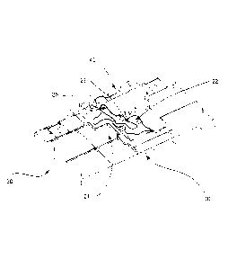
Referring to figure 1, we present a classic assembly of a memory card reader.
This memory card reader comprises a memory card reader body 10 comprising a
memory card insertion slot 11. The memory card connector is directly
integrated into
the memory card reader. It comprises pins 12 for connection to the printed
circuit board
(PCB) 13 (seen in a partial view). The PCB 13 also has electronic components
14. To
protect the memory card reader 10, it is covered with a full protective
coating 15 as well
as a front protective coating 15b.
There is therefore a need for providing a memory card reading architecture
that
is intrinsically secured and does not require complementary protection.
3. Summary of the invention
The invention thus relates to a memory card reader body.
More particularly, the invention relates to a memory card reader body with an
overall rectangular parallelepiped shape comprising a slot for inserting a
memory card.
According to the invention, such a reader body comprises, on a rear face 21, a
housing for receiving a memory card connector, said housing for receiving
having a
predetermined volume shape and comprising at least one conductive track.
Thus, the invention facilitates the assembly. Indeed, owing to the
configuration
of the memory card reader body, the invention makes it possible first of all
to weld the
memory card connector to the PCB and then to fix the body of the memory card
reader
to the PCB in covering the memory card connector. In a complementary way, this
memory card reader architecture also makes it possible to fix other components
to the
PCB, the body of the memory card reader subsequently covering also the other
components. In addition, since the housing for receiving comprises a device
for
protecting said memory card connector, it becomes extremely difficult to
penetrate the
device in proximity to the memory card connector. the rear face of the body of
the
reader is the one intended to cover the memory card connector when the unit is
mounted
on a destination PCB.
According to one particular characteristic, said volume shape of said housing
for
receiving is substantially equal to the volume shape of the memory card
connector.
3
CA 02889115 2015-04-21
Thus, the invention limits the volume left free between the housing of the
body
of the memory card reader and the memory card connector. More particularly,
the
volume left free corresponds to the volume needed for the passage of the
memory card.
According to one particular characteristic, said rear face of said memory card
reader body furthermore comprises at least one complementary housing to
receive at
least one electronic component.
Thus, the invention also provides for a protection of one or more
complementary
electronic components that are covered by the memory card reader when it is
fixed to
the PCB.
According to one particular characteristic, in said housing for receiving,
said
memory card reader body comprises at least one protective circuit.
According to the invention, such a body of the memory card reader comprises.
on the rear face of the body of the reader, also called an internal face, at
least one
protective track, this track covering at least one surface appreciably
equivalent to a
.. volume of a free space in said memory card reader body.
Thus, according to the invention, it is no longer necessary to have available
a
protective flexible piece over the body of the memory card reader. Indeed,
according to
the invention, the body of the reader of the memory card directly integrates
the track or
tracks that fulfill the same function as the protective flexible piece and the
front
protection. In addition, since it is no longer necessary to have the
protective elements of
the prior art, the invention simplifies the mounting of the reader terminal
since it
eliminates several mounting steps and also eliminates the cost of these
protections.
According to one particular embodiment, said protective circuit takes the form
of at least one lattice comprising said at least one conductive track.
According to one particular embodiment, said protective circuit takes the form
of at least one continuous electrical track comprising said at least one
conductive track.
For example, this track can be obtained by the use of the technique known as
the
molded interconnected device (MID) technique or by other methods.
4
According to one particular embodiment, said protective circuit is made by
means of a laser etching technique.
This laser etching technique is coupled with chemical baths and is called
laser
direct structuring or LDS.
According to one particular characteristic, said protective circuit is a
flexible
printed circuit positioned within said housing for receiving.
According to one particular characteristic, said rear face of said memory card
reader comprises at least one complementary housing for receiving at least one
electronic component and said complementary housing is positioned beneath said
protective circuit.
According to one particular characteristic, said at least one conductive track
is
shaped to define electrostatic discharge zones coming into contact with a
smart card
when said smart card is introduced into said reader body.
The invention also relates to a memory card 'reader terminal. According to the
invention, such a terminal comprises a body of the memory card reader as
described
here above.
4. Figures
Other features and advantages of the invention shall appear more clearly from
the following description of one preferred embodiment, given by way of a
simple,
illustratory and non-exhaustive example, and from the appended drawings, of
which:
Figure 1, already presented, describes the classic architecture of a memory
card
reader,
Figure 2 illustrates the general principle of the invention, namely the
separation
of the memory card connector and of the memory card reader body into two
distinct functional units;
Figures 3 and 4 illustrate one embodiment of the invention in which the body
of
the memory card reader comprises an intrusion detection track.
5
CA 2889115 2019-10-15
5. Detailed description
5.1. Reminder of the principle of the invention
The general principle of the invention consists in proposing an architecture
of a
memory card reader that directly integrates the functional constraints
inherent in the
working of this type of device. More particularly, the general principle of
the invention
consists in the subdivision of the memory card reader into two distinct parts.
There is a
first part through which the memory card signals travel in transit, this part
including the
switch for detecting the presence of a card. This first part is capable of
ensuring a
residual portion of the electrostatic discharge (from the memory card
connector). There
is then a second part enabling the insertion of the memory card. This second
part
ensures firstly the guidance of the memory card and the absorption of the
memory card
forces. Secondly it carries out a part of the electrostatic discharging of the
card. This
second part also ensures protection of the signals exchanged between the
memory card
and the memory card connector (this is the body of the memory card reader
proper).
The general principle of the invention is described with reference to figure
2.
According to the invention, a memory card connector 10 is built independently
of the
memory card reader body 20. The memory card connector 10 is designed to enable
a
reading of the signals coming from the memory card (not shown). In figure 1,
the
memory card connector 10 is designed for the reading of a smart card. To this
end, the
memory card connector 10 comprises a certain number of pins 11 (eight in
figure 2)
used to come into contact with corresponding zones of the memory card (six or
eight
zones depending on the memory card). The pins 11 are generally metal spring
blades
positioned on the surface of the chip. Since the object of the disclosure is
not this
connector, it shall not be described in detail here below.
According to the invention, on the contrary, this memory smart card 10 is
independent of the memory card reader body 20. This means that, unlike in the
prior-art
systems, the memory card connector 10 is not assembled with the body of the
memory
card reader 20 before being assembled with the PCB of the reader terminal. The
6
CA 2889115 2019-10-15
CA 02889115 2015-04-21
invention proposes firstly to fix the memory card connector 10 to the PCB and
then to
fix the body of the memory card reader 20 over the connector 10. In other
words, it will
be understood that this assembly is not at all of the same nature as the
assembly of the
prior art since the memory card connector is covered by the body of the memory
card
reader which, so to speak, protects it. In other fields, there are known
terminals in which
the lower cover of the terminal (i.e. its external casing) acts as the reader
body.
However, unlike in the invention, this cover is not protected and is not used
to carry out
a securing procedure. This reader body has no track and does not fulfill the
functions
described here. More particularly, this reader body has no track whether on
its rear face
to protect the terminal or in any other portion of the reader in order for
example to carry
out an electrostatic discharge of the memory card prior to its insertion.
Additionally, in at least one embodiment, the invention proposes to eliminate
the
protective flexible piece which entirely covers the memory card reader. In one
embodiment, the invention replaces this protective flexible piece by an
internal
protective device, i.e. one that is situated inside the memory card reader
body 20 itself.
Here below, one specific embodiment of the invention is described. It is
understood that this embodiment in no way restricts the scope of the
invention. More
particularly, in other embodiments of the invention, the memory card connector
can be
protected by using means for etching electrical tracks other than those
described here
below (for example a flexible circuit bonded to the interior of the body of
the reader).
5.2. Detailed description of one embodiment
In this embodiment, an internal protective device is positioned in the body of
the
memory card reader. In this embodiment, the protective device takes the form
of
electrical tracks integrated into the body of the memory card reader 20 in
proximity to
the contact zones of the pins of the memory card connector 1 0 when the body
of the
memory card reader covers the memory card connector.
This embodiment is presented more particularly with reference to figures 2 and
3. As indicated here above, a complementary part (the body of the memory card
reader
20) is added above the memory card connector. In this embodiment of the
invention, the
body of the memory card reader 20 is a part made of plastic. In addition to
its functions
7
CA 02889115 2015-04-21
=
of insertion and holding and of absorbing the stresses in the memory card, for
example
the smart card, the body of the memory card reader 20 also protects the I/0
signal
travelling in transit through the memory card (smart card) and the memory card
connector 10, as closely as possible to the signal to be protected (the
structured surface
is therefore smaller and the protection is better than with a flexible
shielding external to
the memory card reader).
In this embodiment, the body of the memory card reader 20 is a part with a
generally rectangular parallelepiped shape, a width of about 60 millimeters, a
depth of
about 40 millimeters, and a height of about 4 millimeters. The body of the
memory card
reader 20 comprises an insertion slot 30, with a height of 0.8 to 1.5
millimeters. The
insertion slot 30 enables the insertion of the memory card in an accurate
position so that
it comes into contact with the memory card connector 10. The memory card
reader also
has, on its rear face 20, a housing 22 intended to receive and cover the
memory card
connector 10. The volume shape of this housing for receiving 22 is appreciably
complementary to the volume shape of the memory card connector 10, without
counting
the space needed for the presence of the memory card. Thus, the memory card
connector 10 and more specifically the tracks through which the 1/0 signals
travel are
covered by the body of the memory card reader 20. In addition, in the housing
22. the
body of the memory card reader comprises at least one protective circuit 23.
This
protective circuit 23 can be a 3D circuit. This protective circuit 23 for
example takes the
form of one or more intrusion detection lattices or the foi _______________
III of one or more continuous
intrusion detection tracks (for example a ground circuit, and two lattices at
different
potentials). This protective circuit 23 is positioned in the housing 22 on the
rear face of
the memory card. It is also positioned on the side edges 24 of the housing.
Besides, the
protective circuit is stepped: it means that the protective circuit 23 is not
situated in a
single plane but in several (at least two) planes. Thus, it is ensured that
the protective
circuit 23 appreciably covers the volume shape of the memory card connector
10. In this
embodiment, the memory card reader body 20 furthermore comprises at least one
complementary housing 40 for receiving at least one electronic component.
More particularly, the body of the memory card reader, in one particular
embodiment of the invention, is a part called an MID (molded interconnect
device).
8
CA 02889115 2015-04-21
More particularly, the body of the memory card reader MID protects two
surfaces in
opposite parts. Indeed, a laser etching is done in order to produce 3D
electronic tracks.
The use of this technique is unusual in the field of the invention.
In one embodiment, the part made by LDS (laser direct structuring) has an
internal surface which is extended to an upper part (reference 24 in figures 2
and 3)
enabling complete protection in MID, in every direction. In this embodiment of
the
invention, the MID etching enables the making of one or more lattices, said
lattice or
lattices being classically a protection enabling the detection of the
insertion of a device
into the body of the memory card reader. The use of a lattice to detect an
insertion or an
attempt at drilling is a technique known in the field of the invention.
However, unlike in
the prior art, the invention directly integrates the lattice into the internal
surface of the
memory card connector and does so in a highly integrated manner.
In other words, the laser etching is done in three dimensions in order to be
in
keeping with a volume of the memory card connector and more particularly to be
situated in proximity to the sending/reception of signals coming from the
card. Thus, a
3D lattice is defined. This 3D lattice is adapted to the shape of the memory
card
connector. There is no longer an excessively sized flexible piece or another
element for
the front protection given the zone to be protected.
More particularly, the distance between the etching defining the protective
tracks
and the pins of the memory card connector is about one-tenth of a millimeter.
It will therefore be understood that, with this magnitude of size, it is
appreciably
more complicated to make an attack on the memory card connector in trying to
insert a
device. Thus, in only one part, the invention makes it possible to bring down
the
protection to the lower part of the connector (the recessed or undercut
portion) in adding
.. neither a complementary phase nor an intermediate connection.
The body of the reader also resolves the problems related to the stopping the
card upon insertion. It does not require that the card should be stopped by
the electrical
connector which for its part carries only the fastenings to the electronic
printed circuit,
which are soldered by rellow soldering (and therefore are fairly fragile with
respect to
the stresses generally observed).
9
CA 02889115 2015-04-21
It must also be noted that the body of the reader can be formed of two parts
that
can be clipped together with a link between the two parts which can overlap
each other,
and that there is no possibility of subsequent separation (except by damaging
the lattice
and therefore activating a protective response). In this case, the lattice or
lattices can
also be bigger because it is no longer necessary for them to be visible, for
reasons of
manufacturing process.
5.3. Complementary characteristics
In certain embodiments, which may or may not be combined with the
characteristics described here above, the body of the memory card reader as
defined
comprises a discharge zone (called an ESD zone) enabling a first discharging
of the
memory card when it is inserted into the reader. More particularly, in order
to preserve
the property whereby the body of the memory card connector is a single piece,
this
electrostatic discharge zone is produced by using MID technology. In a first
embodiment, this discharge zone is situated in proximity to the zone of
insertion of the
memory card, appreciably at the position where the chip of the memory card is
situated
during the insertion. More particularly, the body of the reader is configured
so that the
chip of the card comes into contact with this discharge zone.
In this second embodiment, this discharging zone is situated within the body
of
the reader, more particularly on the internal face of the flanks of the body
of the reader.
More particularly, the internal face of the flanks of the body of the reader
is configured
so that at least one edge of the card comes into contact with this discharging
zone.
According to another characteristic, in order to avoid the problems related to
the
welding of the protective lattice (on the inner face of the body of the memory
card
connector) to the PCB, the connection between these two elements is done by
means of
an elastomeric connector, for example of the Zebra (registered mark) type.
Thus, it is
not necessary to available complicated mechanisms for welding the body of the
memory
card reader to the PCB: indeed, since the connection is provided by means of
an
elastomeric connector, the mounting of the unit formed by the memory card
connector,
the elastomeric connector and the body of the memory card reader is
facilitated.
10
CA 02889115 2015-04-21
More generally, to facilitate the assembly, the following steps are
implemented:
a step for fastening the memory card connector to the PCB. This fastening can
be done by screwing in or by soldering or by bonding or by a combination of
these methods. Other fastening methods can also be used.
- a step for positioning the elastomeric connector (when it is used). The
positioning of the elastomeric connector can advantageously be done in a zone
left free for this purpose within the memory card connector.
a step for positioning and fastening the body of the memory card reader with a
mode of fastening of the body of the reader relatively to the PCB. In the case
of
Zebra, a screw fixed to a part of the memory card connector is an advantageous
solution or again the addition of a fifth pin acting as a mechanical holding
piece.
Thus, two or three steps only are needed to assemble and fix the memory card
reader to the PCB.
5.4. Description of one embodiment of a memory card reader
This embodiment is more particularly described with reference to figure 4. For
greater simplicity, the numerical references that have been previously used in
figures 2
and 3 are kept. In this embodiment, the memory card reader comprises a memory
card
reader body 20, a memory card connector 10, and an elastomcric connector 30.
The
architecture of the memory card connector 10 is built so that it comprises a
space FCE
left free for the positioning of the elastomeric connector 30. Thus, during
the
assembling, the memory card connector 10 is first of all fixed to the PCB and
then the
elastomeric connector 30 is inserted into the space ECE. The body of the
memory card
reader 20 is then positioned above the unit formed by the memory card
connector and
the elastomeric connector. As already mentioned, the body of the memory card
connector 20 comprises a zone for discharging the card 24. The memory card
reader 20
is fixed to the PCB by means of a screw 26 and four anchoring slugs 27. The
screw 26
also serves to maintain permanent pressure over time. The screw 26 is screwed
into the
memory card connector which is itself fixed to the PCI3 by soldering. The link
is
therefore direct. The anchoring slugs have a particular shape adapted on the
one hand to
11
CA 02889115 2015-04-21
A
fulfilling a function of guiding the memory card in the reader and, on the
other hand, if
necessary, to carry out an electrostatic discharging of the edges of the
inserted card.
In addition, in this system, the centering between the memory card connector
and the body of the memory card reader enable the positioning to be done in a
rigorous
way.
Indeed, in this embodiment, the memory card connector comprises at least two
centering holes. The centering holes are configured so that the centering pins
which are
integrated into the body of the memory card reader can take position in the
centering
holes. Thus, in this embodiment, it is not possible to carry out an erroneous
mounting of
the memory card reader. More particularly, it is not possible to position the
body of the
memory card reader with an incorrect angle relative to the connector.
12