Note: Descriptions are shown in the official language in which they were submitted.
CA 02890261 2015-04-27
WO 2014/074122 PCMJS2012/072337
HIGH ENERGY DENSITY ELECTROSTATIC CAPACITOR
FIELD OF THE INVENTION
This invention relates generally to capacitors, and, more particularly, to a
high energy
density capacitor with a dielectric layer between augmented permittivity
polymer layers.
BACKGROUND
Methods for the manufacture of capacitors are varied depending upon the nature
of the
capacitor and the energy storage requirements. In electronics, low dissipation
factor and
small size are primary requirements. In other applications the size of the
energy storage
device is less important than cost. In yet other applications, rapid delivery
of the energy
stored in the capacitor is a paramount concern.
In the field of energy storage, capacitors are generally recognized as
advantageous. In
the past, pure electrostatic capacitors have usually been the least energy
dense and one of the
most expensive devices to store bulk energy. Despite their limitations,
electrostatic
capacitors have found widespread use in electronics due to their ability to
deliver very high
power rates. This very attractive feature is due to the ways in which the
power is stored
within the capacitor. For example, since the discharge of a capacitor does not
generally
depend upon the movement of electrochemical species in a relatively macro
environment, the
power delivered by a capacitor is generally at least several orders of
magnitude greater than a
similarly sized electrochemical battery.
Capacitors are also generally able to withstand relatively low temperatures
and
relatively high temperatures. Many types of capacitors perform in temperature
ranges of -
C to 120 C. Extension of these ranges with controlled or linear capacitances
is also a
desirable feature.
Unfortunately, capacitors are also generally characterized by high cost per
unit energy
25 stored per volume or weight. Use of electrostatic capacitors for bulk
energy storage has been
severely hampered by the high unit costs in this application. A reduction in
the unit cost per
unit energy stored is desperately needed by the world's increasing needs for
energy storage.
By way of background, assuming a 1 cubic meter volume and using units of the
mks
system, it can be shown that energy is proportional to permittivity and
inversely proportional
30 to the square of the thickness or distance between electrodes, as
follows:
eoKV 2 eoKE 2
U=
2d2 2
1
CA 02890261 2015-04-27
WO 2014/074122 PCT/US2012/072337
where, U = energy
V = Voltage between the electrodes
d = distance between electrodes
K = Relative Permittivity
e0 = permittivity of vacuum
E = Electric Field (V/d)
The thinnest dielectric at the highest voltage possible (largest E-field) will
provide the
highest energy density possible at a given relative permittivity, K. The
highest voltage
possible varies greatly depending upon the material used for the dielectric.
To obtain the
highest energy storage levels, the dielectric should be very nonconductive,
have a good
permittivity and be as thin as possible.
Any conductivity between the electrodes is termed leakage current and is to be
avoided.
At some voltage level the dielectric will become conductive, by either the
leakage current
rising to unacceptable levels or the leakage current rising dramatically in a
fraction of a
second (usually accompanied by a plasma spark). The limit of the E-field value
varies
greatly depending upon the molecular chemical nature of the dielectric and the
morphology
of the dielectric material.
As a general rule the more polar a molecule in the dielectric, the higher the
dielectric
constant (i.e., relative permittivity). And, as a general rule the high
dielectric breakdown
voltage materials tend to have low permittivity. Exceptions to those general
rules are certain
compounds, such as barium titanate or other Perovskite types of mixed metal
oxides
(ceramics). Those types of compounds we can see both high permittivity and
good resistance
to dielectric voltage breakdown. However, another problem then occurs when
these types of
dielectrics are pushed to energy storage levels that are beyond their
capabilities. In particular,
metal oxide ceramics have difficulty maintaining high permittivity at large E-
fields
(voltages). As an example, it has often been found that the permittivity of
barium titanate at
high E-fields results in an over 100 times reduction in permittivity versus
the low E-field
permittivity. Thus, the need for a high E-field breakdown material with
simultaneous high
permittivity is needed in electrostatic capacitor devices. It is therefore
important that the
voltage rating for the capacitor be as high as possible when energy storage is
the primary use
for the device.
In addition to having a high break down voltage, a high energy density
capacitor should
also possess an extremely low leakage current. Thus, when the capacitor has
been charged to
2
CA 02890261 2015-04-27
WO 2014/074122 PCT/US2012/072337
a given voltage, the rate of charge conduction from one electrode to the other
should be a
relatively small value. When the capacitor is charged for energy storage over
a given period
of time, the rate of leakage is an acceptably low enough value that would vary
depending on
the use of the storage device (how long is it stored) and the "value" of the
energy thus stored
(how easy is it to recharge and the cost of the charge). While an acceptable
value for leakage
may vary greatly from application to application, leakage is undesirable and
to be avoided
and minimized.
Heretofore it has been recognized that the addition of insulative materials to
the
dielectric matrix can cause an unwanted diminution in the value of the
dielectric breakdown
strength. In general this is true. Also the construction of a capacitor is
governed by the
geometric construction of the device. A multilayer dielectric is generally not
preferred for a
film capacitor. Setting aside the complications involved in forming several
layers between
the electrodes for the dielectric, the overall gain of energy storage is
usually little if any. This
is caused by the reduction in the E-field that is necessary when the layers
are diminished in
thickness.
Due to the desirable characteristics of electrostatic capacitors and other
undesirable
features, an improvement in the methods and materials for the construction of
these energy
storage device and improved capacitors incorporating these materials are
needed. The
invention is directed to overcoming one or more of the problems and solving
one or more of
the needs as set forth above.
SUMMARY OF THE INVENTION
To solve one or more of the problems set forth above, in an exemplary
implementation
of the invention, a solid state electrical energy state storage device, such
as a capacitor,
includes a pair of conductive electrodes, i.e., a first electrode and a second
electrode. The
first electrode and second electrode are parallel and spaced apart by an
intervening space. A
primary dielectric comprised of a primary dielectric material is disposed
between the pair of
conductive electrodes within the intervening space. The primary dielectric has
a first surface
adjacent to the first electrode and an opposite second surface adjacent to the
second electrode.
The secondary dielectric layer is comprised of a secondary dielectric material
and is disposed
between and in contact with the first surface of the primary dielectric and
the first electrode.
The secondary dielectric layer has an augmented permittivity, i.e., a
permittivity that is
augmented by exposing the dielectric to a magnetic field and/or an electric
field during
formation of the dielectric material, before the dielectric material has fully
solidified. The
3
CA 02890261 2015-04-27
WO 2014/074122 PCT/US2012/072337
tertiary dielectric layer may also have an augmented permittivity. The
permittivity and
composition of the secondary and/or tertiary dielectric layers may be
different from the
permittivity of the primary dielectric. The permittivity and composition of
the secondary and
tertiary dielectric layers may be, but do not have to be, the same. The
secondary and tertiary
dielectric layers may thin films having thicknesses that are substantially
less than the primary
thickness of the primary dielectric. The secondary and tertiary dielectric
layers may
comprised of an insulating polymer, such as a xylene based polymer. Further,
the xylene
based polymer may be a puralene polymer, which is a new xylene based polymer
formed
under atmospheric conditions via reaction with monatomic oxygen and provided
an
augmented permittivity through exposure of the polymer to a magnetic field
and/or an
electric field during condensation and solidification on a substrate. Exposure
to an electric
field provides an electric field ordered solid matrix. Exposure to a magnetic
field induces
radical intermediate species and attendant increases in permittivity.
In another embodiment, the solid state electrical energy state storage device
includes an
integrally formed heterogeneous dielectric disposed between the pair of
conductive
electrodes. In this embodiment, the dielectric has different compositions
(e.g., different
concentrations of constituents) through its volume, and different
permittivities through its
volume.
By way of example, the integrally formed heterogeneous dielectric may have a
first
portion including a first surface and a first composition, a central portion
and a second
portion including a second surface opposite the first surface and a second
composition. The
first surface is adjacent to and in contact with the first electrode. The
opposite second surface
is adjacent to and in contact with the second electrode. The central portion
has a central
composition and is disposed between the first portion and the second portion.
The central
composition has a central average permittivity. The first composition has a
first average
permittivity. The second composition has a second average permittivity. The
first and
second average permittivities may be the same augmented permittivity (e.g.,
electric field
and/or magnetic field augmented permittivity) and may be different from the
central average
permittivity.
4
BRIEF DESCRIPTION OF THE DRAWINGS
The foregoing and other aspects, objects, features and advantages of the
invention will
become better understood with reference to the following description, appended
claims, and
accompanying drawings, where:
Figure 1 is a side view of an exemplary capacitor that may contain conductive
and
dielectric elements according to principles of the invention; and
Figure 2 is a perspective view of an exemplary capacitor that may contain
conductive
and dielectric elements according to principles of the invention; and
Figure 3 is a high level flowchart that illustrates an exemplary method of
producing an
augmented permittivity material for use in a capacitor according to principles
of the invention;
and
Figure 4 is a schematic that conceptually illustrates an exemplary structure
comprising
layers of materials for a capacitor according to principles of the invention;
and
Figure 5 is a schematic that conceptually illustrates another exemplary
structure
comprising layers of materials for a capacitor according to principles of the
invention.
Those skilled in the art will appreciate that the figures are not intended to
be drawn to
any particular scale; nor are the figures intended to illustrate every
embodiment of the
invention. The invention is not limited to the exemplary embodiments depicted
in the figures
or the specific components, configurations, shapes, relative sizes, ornamental
aspects or
proportions as shown in the figures.
DETAILED DESCRIPTION
In a capacitor with a multilayer dielectric between two electrodes, where each
dielectric
layer may have distinct relative permittivity, the overall permittivity is the
following:
I f fb f, a +
K Ka Kb lc
Where K = overall relative permittivity
fx = volume fraction percent of layer x
Kx = relative permittivity of layer x
The lowest permittivity layer predominates in the calculations to a very large
extent when
the volume fractions of the layers are relatively equal. However, when the
volume fraction
percent of the low permittivity material is small and permittivity of the
larger bulk layer is
large, then the overall permittivity of the device is less substantially
compromised by the low
permittivity material. This is illustrated in the table below.
5
CA 2890261 2018-02-14
CA 02890261 2015-04-27
WO 2014/074122 PCT/US2012/072337
Permittivity (K)
3.0 6.0 12.0
of layer a
Permittivity (K)
20000.0 20000.0 20000.0
of layer b
fa it;
0.1 0.9 30.0 59.8 119.4
0.2 0.8 15.0 30.0 59.9
Table 1.
Thus, if the volume fractions are chosen carefully and relative permittivity
of the layers
is optimized, then vast improvement of the dielectric can take place.
Heretofore these
improvements have not been realized due to the processes, materials, and the
methods
defined herein having not been invented.
The aforementioned results are tempered by the ability of the dielectric to
withstand
substantial E-fields without dielectric breakdown or excessive leakage
currents. Thus, the
benefit of energy storage improvements in the permittivity can be completely
negated by a
reduction in the working E-field values.
A common misconception is that the permittivity of a given material is linear
to the
point of its breakdown voltage. Extreme non-linearity in permittivity is
usually found. In
certain cases (e.g., barium titanate) the reduction in permittivity can be
over 100 times the
low field value. Thus, increases in E-field are less productive in traditional
capacitor design
than thought.
A previously known general class of energy storage devices is referred to as
HED
(High Energy Density) capacitors. These capacitors are electrostatic
capacitors that are
different from EDLC (Electrical Double Layer Capacitor) type of capacitors
commonly
referred to as supercapacitors or ultracapacitors. As the design, manufacture,
and
performance of the energy storage devices disclosed herein differ in
construction, materials,
and overall performance so much from previously known devices for energy
storage, a new
term for these devices is used herein. The acronym SHED (Super High Energy
Density) is a
name given to a capacitor having a structure and composition according to
principles of the
invention. SHED capacitors have properties and a design that are most closely
related to
traditional electrostatic capacitors. Concomitantly, SHED capacitors have
performance
6
characteristics that are normally associated with polymer film capacitors, but
the energy
densities are vastly greater than that of traditional film capacitors by
orders of magnitude.
Additionally, in the case of a SHED capacitor, reduced E-fields are present in
the bulk
dielectric and permittivity is linear with E-field. This enables substantially
increased energy
storage.
In a preferred embodiment, substantial improvements in the voltage rating,
leakage
current, and dielectric permittivity of an energy storage capacitor are
realized. While the
improvements as described herein relate to the field of energy storage, the
methods and devices
disclosed herein may be applied to other devices, imparting improved frequency
response and
reduced dielectric absorption.
In one or more embodiments, a high permittivity low leakage capacitor and
energy
storage device is described having the following improved characteristics:
1) High voltage rating (High break-down E-field),
2) High relative permittivity,
3) Low leakage current at maximum voltage charge,
4) Small size and weight,
5) Safe use due to low toxicity and other hazards,
6) Easy and better manufacturing procedures,
7) Environmentally friendly manufacturing,
8) High rate of discharge and charge, and
9) Ability to fully discharge their electrical energy.
A process for manufacturing high permittivity high quality materials for use
in a
capacitor according to principles of the invention is also disclosed. Among
the materials is a
material referred to herein as PuraleneTm, which is a compound that possess
the characteristics
of a recognized class of materials known as parylenes. The Puralene class of
materials extends
into materials comprised of polymeric aromatics possessing carbon atoms alpha
to aromatic
moieties within the starting materials. Puralenes are one class of materials
that can be used to
make energy storage devices according to principles of the invention.
The varieties of dielectrics that may be used to form a capacitor are
virtually limitless.
To produce a substantially improved energy storage device, it requires more
than simply
making a dielectric and putting it between two electrodes. The method whereby
the dielectric
is selected, transformed, and applied is important and not obvious to those
skilled in the art of
electrostatic capacitor manufacture. Additionally, embodiments are described
whereby
7
CA 2890261 2018-02-14
CA 02890261 2015-04-27
WO 2014/074122 PCT/US2012/072337
certain known methods of manufacture which are commonly discounted as being
unattractive
methods of process are shown to be actually superior methods for the
production of high
energy density electrostatic capacitors.
During manufacture a magnetic or electric field or both may imposed upon the
dielectric material, i.e., the dielectric material may be exposed to such
fields as part of the
manufacturing process. The exposure to an electric or magnetic field during
processing
results in a different material that exhibits increased permittivity, i.e.,
augmented permittivity.
At low electric field potentials, the increase in permittivity is
proportionally increased with
the increase in the electric field potential. In some salts of inorganic metal
ions the increase
in the permittivity is achieved when exposed to a magnetic field.
Additionally, exposure to
magnetic fields enhances permittivity of organic compounds.
Simultaneous utilization of an electric field and a magnetic field can help
reduce the
requirements for the strength of either field with materials that respond to
the magnetic field.
When electric field strengths of almost any magnitude are impressed upon the
dielectric,
before full solidification, while the dielectric is in a pliable or less
viscous state, an increase
in the permittivity of the resulting dielectric is achieved. This is made
possible using the low
temperature processes described herein. Electric field strengths greater than
100 V/micron
provide greater than 100% improvement in the permittivities of several
different organic and
inorganic dielectrics.
Magnetic fields may also be used to cause increases in the permittivities.
Even a
relatively small magnetic field (e.g., about 1 Gauss) has caused observable
increases in the
permittivity of polymeric materials and/or crystallization of polymers, small
molecule
organics, and salts of both inorganic and organic nature. Strong magnetic
fields seem to
induce greater amounts of permittivity increases than weak fields.
Permittivities in the range
of 7 to >2000 and improvements in permittivities from normal range from 5% to
>6000%
have been observed utilizing the methods taught.
In the case of a molecule in which there is substantial polarization and/or
separation of
charge due to zwitterionic structures, the acid and the base may be contained
within the
molecule itself. In those cases, high dielectric polarization may be achieved
within a single
molecule. Good permittivities may be obtained with amino acids where an acid
and base
chemical moiety is found. However, in many protein matrices, ionic forms may
be
encapsulated with the protein backbone. In the case of the protein zein, this
structure is
8
CA 02890261 2015-04-27
WO 2014/074122 PCT/US2012/072337
believed to produce a high permittivity dielectric when solidified under a
magnetic and/or
electric field.
The following representative embodiments, set forth specific examples of
methods of
making a high permittivity material in accordance with the present disclosure.
It is
understood that the disclosure need not be limited to the disclosed
embodiments but it is
intended to cover various modifications thereof, including combinations of the
steps and
components of the various examples.
Referring now to Figures 1 and 2, a conventional form of a capacitor
(originally known
as condenser) is conceptually illustrated. The capacitor includes housing
which contains a
dielectric material disposed between a pair of opposed plates, referred to as
electrodes.
Connecting leads extend from the electrodes. The configuration and arrangement
of the
housing, connecting leads, plates and dielectric material may have many
variations. While
the invention may be applied to a capacitor of the type illustrated in Figures
1 and 2, the
invention is not limited to such a particular capacitor configuration.
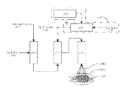
Referring now to Figure 3, a high level flowchart that illustrates an
exemplary method
of producing an augmented permittivity material, e.g., Puralene, for use in a
capacitor
according to principles of the invention is shown. Sections, referred to
chambers, may
comprise tanks having an inlet and an outlet or tubular structures with an
inlet and an outlet.
Chamber 210 is a heated tube or other evaporation device to volatilize
starting material feed
200. Starting material feed 200 is evaporated and mixed with inert gas 205 in
chamber 210.
Inert gas 205 may be any of a group of inert gases, such as, but not limited
to, Argon.
Substitution of nitrogen for argon and/or other essentially inert gases is
possible. Pumps and
valves may be used to propel and control the flow of fluids from one station
to another.
By way of example and not limitation, chamber 210 may comprise an electrically
heated Inconel (nickel alloy 600) pyrolysis reaction tube. The tube is heated
to a temperature
of about 450 C to 630 C at atmospheric pressure. A flowing stream of argon gas
alone, or
with a reactive compound such as nitrous oxide, is supplied to the pyrolysis
reaction tube.
The starter material feed 200 may be xylene vapor (Aldrich #134449-4L). If the
carrier gas
205 includes a reactive compound (e.g., N20), the ratio of gases is adjusted
to provide
approximately molar stoichiometric ratios of 1:1 (xylene to nitrous oxide).
The heated starter material 200 in the volatile mixture with inert gas reacts
with
monatomic oxygen in reaction chamber 215. Being very reactive and transient,
monatomic
oxygen must be available to react with the volatile mixture in the reaction
chamber 215. As
9
CA 02890261 2015-04-27
WO 2014/074122 PCT/US2012/072337
discussed above, the source of monatomic oxygen may be a gaseous compound
supplied with
the carrier gas 205, or a gaseous compound supplied separately 240, or another
source, such
as a plasma generator 235.
Monatomic oxygen plasma may be created by exposing oxygen (02) gas at a low
pressure to a high power energy source, such as an RF discharge, which ionizes
the gas.
Alternatively, a compound such as Nitrous Oxide (N20) may supply monatomic
oxygen for
the reaction. Thus, a monatomic oxygen plasma generator 235, or a monatomic
oxygen
chemical compound (e.g., N20) feed 240, or another suitable source of
monatomic oxygen is
provided.
A plasma gas can be used with the aforementioned starting materials to form
the
intermediate oxidized products that may subsequently react to form reaction
products that are
oxidized forms of the starting materials which may be monomers, dimers,
trimers, oligomers,
or polymers. The plasma generator 235 includes a gas feed 230 that supplies
gas to a plasma
reaction chamber 220. A plasma driver 225 provides high power energy to ionize
the gas.
The ratio of gases is adjusted to provide approximately molar stoichiometric
ratios of
1:1 (xylene to nitrous oxide or xylene to monatomic oxygen plasma).
Illustratively, increased
amounts of nitrous oxide result in partial and/or complete oxidation of xylene
with reduced
formation of the desired cyclophane or its polymer. Close control of the
stoichiometry is
desired in this gas phase reaction.
The reaction products are supplied to a reaction chamber 235, which is heated
to
approximately 450 C to 800 C to facilitate vaporization of the reaction
products. The
vaporized reaction products 245are expelled onto a low temperature collection
surface 250,
where the reaction products condense and form a solid. At higher temperatures
(650 C to
800 C) the output of the reaction chamber 235 is sufficiently hot enough to
maintain the
monomeric p-xylylene in monomeric form.
Condensation of the gas onto a cooled glass vessel resulted in the deposition
of a
colorless to cream colored solid. This solid is partially soluble in 95%
ethanol. The solid was
compared to a sample of [2,2 1paracyclophane (Aldrich #P225-5G-A) by GC
analysis
(SRI#310, 15m, megabore column, FID detector) and was shown to give identical
retention
times.
Rapidly cooling of the monomer onto a surface 250 results in a liquid
condensation of
the monomer and rapid polymerization of the monomer into a polymer. Comparison
of the
film thus produced appears to be identical to parylene film produced by the
Gorham process.
CA 02890261 2015-04-27
WO 2014/074122 PCT/US2012/072337
Without augmentation, permittivity of the solidified product is about 3,
electric breakdown
strengths are about identical at 100 V/micron, and solubility in both hot and
cold solvents are
below detectable levels.
In this reaction it is believed that the reactive p-xylylene reactive
intermediate is formed
and subsequently dimerized in the reaction tube 235 or during condensation 245
onto the
substrate 250. This reaction used to synthesize the dimer, in comparison with
the known
"Gorham process", results in a vast improvement in the overall synthesis yield
of the dimer
and also results in a vast improvement in the purity of the dimer directly
from the reaction. It
is understood that variation in the stoichiometric amounts of the reactants
may be adjusted to
provide for greater or lesser yield with associated purities varying to
provide a more
economical process or better overall production efficiency without
substantially deviating
from the scope of this invention. Subsequent purifications of the materials
from this reaction
can be performed on this material in a manner that is much easier to
accomplish than with
previously taught processes. The reaction is shown below.
pyrolysis, 450'3 to
r,;,-.. \Nr======CH3 63 Er C, I. Oa tv,
11 gas ficm ¨
Y'`'''''.-
"3 __ 1.=./ = eõ. ,4'
_ - Hiz -%',
+ 1i2 +1-1:,0
As the reaction temperature at station 235 is increased to >650 C, the
deposition of the
xylylene monomer can proceed directly onto a solid substrate target without
necessity for
isolating the intermediate dimer. Deposition of the exit gas at above 650 C
reaction
temperature upon a cool glass plate resulted in formation of an ethanol
insoluble substance
that displays characteristics of a parylene polymer. However, solubility
characteristics clearly
show that the material is insoluble in all common solvents (i.e. hexane,
xylene, ethyl acetate,
ethanol, water).
It is believed that the reaction mechanism proceeds through a route involving
the prior
decomposition of nitrous oxide. Nitrous oxide is energetically unstable
molecule that can be
thermally decomposed at elevated temperatures. Products of the reaction are
diatomic
nitrogen and monoatomic oxygen. The monoatomic oxygen is able to react with
itself to
form diatomic oxygen, but this reaction is relatively slow. Estimates vary
determining the
temperature that pure thermal decomposition occurs, but estimates of 1100 C
are often cited.
Catalysis of this reaction as shown below in equation 1 is known to occur with
a variety of
11
CA 02890261 2015-04-27
WO 2014/074122 PCT/US2012/072337
metal oxides and mixed metal oxides. Some temperatures used for nitrous oxide
decomposition with certain catalysts are as low as 350 C.
______________________ NN 0(0)
Equation 1
CH3 CH2
0(o)
-I- + H20 Equation 2
CH3 CH2
The reactive species for the process is very likely the monoatomic oxygen
produced
from the decomposition of the nitrous oxide. In this sense, the nitrous oxide
can be viewed as
a convenient carrier for the delivery of the reactive intermediate monoatomic
oxygen.
In a similar manner to the nitrous oxide reaction, pure diatomic oxygen can be
utilized
as a reactant. However, to produce substantial yields of the desired products,
activation of
the oxygen is necessary. It is believed that activation of the oxygen is due
to the excitation of
the oxygen molecule to produce monoatomic oxygen as shown in Equation 3.
[plasma]
0) (0)
0=0 -JP- U 1' 0 Equation 3
The reaction with monoatomic oxygen produced in this manner thus proceeds in a
manner similar to that of the nitrous oxide decomposition route.
Cooling of the elevated temperature gases 245 exiting from the reaction tube
235 is
necessary. If the reaction gas is at too high of a temperature, the ability of
the reactive
intermediate to condense and adhere to a surface is greatly reduced. To this
end, a device to
mix cool nonreactive gases into the hot reaction stream has been devised. The
reaction may
proceed at increased pressure (above atmospheric pressure). Accordingly, an
expansion valve
may be used at the exit of the reaction tube 235 to provide Joule-Thomson
effect cooling of
the hot gas when the gas is below its inversion temperature.
The method may be extended to other substrates such as the ones shown below.
CH
OCH3
CI
faCH3
CI CH3 CH3
H3C' CH3
H3C 'CI
CH3 H3C
1,2,4-TRIMETHYLBENZENE
2-CHLOR0-1,4- 2,5-DICHLORO-PARA- 2,5-DIMETHYLANISOLE
DIMETHYLBENZENE XYLENE
12
CA 02890261 2015-04-27
WO 2014/074122 PCT/US2012/072337
Substituents such as the ones noted above (chloro, dichloro, methoxy, and
methyl) are
not the only aromatic substituents that are capable of being modified by this
process into
reactive intermediates and their subsequent polymers. Additionally,
paracyclophanes and
compounds derived thereof are not exclusive to this process. Meta and ortho
orientation of
the substituents on the aromatic rings are also viable reaction starting
materials. The reaction
can be generalized to include all compounds that are capable of reaction with
monatomic
oxygen produced from a plasma or from decomposed nitrous oxide or its
intermediate
reaction products and also contain hydrogen atoms stabilized by the presence
of an aromatic
ring. Typically such hydrogen atoms are located in a position alpha to a
phenyl ring (benzylic
position). Michael structures removed from the alpha aromatic ring positions
are known to
give similar reactivity to the hydrogen alpha to the aromatic ring position as
is well known to
those versed in organic synthesis. However, the reactivity of such hydrogen
atoms is not
limited to alpha and/or Michael positions from an aromatic ring or the
aromatic ring such as
benzene. Other aromatic stabilization are known for many different rings,
fused rings, and
non-ring systems, as known to those versed in the art of organic chemistry.
Such starting
materials may preferably have the presence of two hydrogen atoms that are
capable of being
removed to form partially oxidized starting materials. These preferred
materials may
optionally have the ability to dimerize, trimerize, oligiomerize, or
polymerize. The
nonlimiting example used herein is p-xylene.
A preferred implementation of the invention augments permittivity of the
polymer by
exposing the condensing reaction products 245 to a magnetic or electric field.
To the output
of the reactions described above, the gaseous stream of reaction product 245
is directed to a
cool solid surface 250. Illustratively, the surface target 250 may be immersed
in a magnetic
field 255 such as that provided by a Neodymium magnet (S84, K&J Magnetics).
Other
magnetic field sources may be utilized and are intended to come within the
scope of the
invention. Condensation of the monomer and subsequent polymerization can
proceed rapidly
while in the magnetic field 255. If the target and the magnet maintain the
same relative
orientation during the polymerization process, then a baseline increase in the
electrical
.. permittivity will occur. If the orientation of the magnetic field 255
relationship to the target
is rotated during the polymerization or solid phase condensation process, then
the resulting
permittivity will be decreased.
13
CA 02890261 2015-04-27
WO 2014/074122 PCT/US2012/072337
When the reaction is conducted as noted above, using the p-xylylene monomer as
the
polymerization molecule, but without the presence of the magnetic field the
relative
permittivity of the material deposited is approximately 3. When the material
is run as
described with a magnetic flux 255 density of approximately 200 to 2000 Gauss,
the relative
permittivity is approximately 7. Thus, the magnetic field substantially
increases the
permittivity by over a factor of 2 times. In a similar manner other salts,
dipoles, and salts of
organic acids can be entropically oriented during solidification or
polymerizations to produce
enhanced high permittivity materials. Improvements in permittivity range from
10 to over
1000% may be attained.
In another implementation, the surface target 250 is immersed in an electric
field 255
such as that provided by a high voltage power supply (G40, Emco, lead spacing
2" at
4000V). Condensation of the monomer and subsequent polymerization can proceed
rapidly
while in the electric field. If the target and the electric field maintain the
same relative
orientation during the polymerization process, then a baseline increase in the
electrical
permittivity will occur. If the orientation of the electric field relationship
to the target is
rotated during the polymerization or solid phase condensation process, then
the resulting
permittivity will be lower.
Condensation of dielectric reaction products in the presence of an electric
and/or
magnetic field, augments the permittivity of the condensed dielectric. This
step may be
.. applied to compounds other than parylene polymers.
When the condensation step is conducted as noted above, using maleic acid salt
with
guanidine as a high dielectric material, but without the presence of the
electric field the
relative permittivity of the material deposited is approximately 500. When the
material is run
as described with an electric field density of 10,000 to 30,000 V/m, the
relative permittivity is
approximately 25000 to 40000. Thus, the electric field substantially increases
the
permittivity by at least a factor of 25 in that particular case. In a similar
manner other salts,
dipoles, and salts of organic acids can be entropically oriented during
solidification or
polymerizations to produce enhanced high permittivity materials. Improvements
in
permittivity range from 50 to over 10000%.
The use of electrical and/or magnetic fields during the condensation process
modifies
the mechanical strength. The material may not be anisotropic after
condensation in strong
fields. Thus, this method is a way of controlling the mechanical properties of
the reaction
products made by this procedure.
14
CA 02890261 2015-04-27
WO 2014/074122 PCT/US2012/072337
Referring now to Figure 4, an exemplary capacitor structure according to
principles of
the invention is conceptually illustrated. A removable carrier film 325 (e.g.,
a polymer film
such as TFE or other non-stick surface material as generally known) is used as
an initial
substrate upon which a conductive coating 305 is deposited. This layer 305 is
the first
electrode. The coating 305 may be aluminum or other conductive metal or
possibly a carbon
coating or conductive polymer. Next, a thin coating of a high permittivity
dielectric material
315, such as a Puralene polymer with augmented permittivity, is applied to the
conductive
coating 305 to provide a nonconductive surface 315 while the conductive
coating 305 retains
its conductivity in the two dimensions perpendicular to the coating plane.
Subsequent to this
step, a thick film of dielectric material 320 may then be applied to this
surface 315 by any of
a variety of methods known to those in the thick film coatings (e.g., screen
coating, spin
coating, vapor deposition, etc.) Optionally, then another thin coating of a
high permittivity
dielectric material 310, such as a Puralene polymer with augmented
permittivity, is applied to
the surface of this dielectric thick film 320. Finally, the exposed surface of
the layers is
coated or put in contact with another conductive layer 300 to form an opposite
electrode from
the first 305. Advantageously, the intermediate thin film dielectric layers
310, 315
substantially enhance overall permittivity in a cost effective manner, without
compromising
break-down E-field or increasing leakage current at maximum voltage charge.
Connection
and mounting of the device thus constructed is well known to those versed in
this art.
An ionization process may be utilized to enable the dielectric 310, 315 to be
applied as
a thin film. An ionizing gas may be fed into a vapor (or atomized) material.
The resulting
material is electrically or magnetically augmented and directed to a removable
carrier film, as
described above. The carrier film has a conductive surface that is oppositely
charged from
the charge of the ionized dielectric. This surface then attracts the
dielectric material 310, 315
to provide a smooth and uniform surface onto which the dielectric may
condense. The
dielectric 310, 315 is condensed in the presence of an electric and/or
magnetic field onto the
conductive surface. After the dielectric 310, 315 is so formed, it may be
applied as a layer of
a capacitor and the carrier film may be removed.
In another embodiment, the dielectric coating 310, 315 is applied by means of
an
ionization process as a thin film. In this embodiment, an ionizing gas is fed
into a vapor (or
atomized) material. The resulting material is electrically charged and
directed to the carrier
film. The carrier film has a conductive surface that is oppositely charged
from the charge of
the ionized dielectric. This surface then attracts the dielectric material to
provide a smooth
CA 02890261 2015-04-27
WO 2014/074122 PCT/US2012/072337
and uniform surface for the dielectric to condense. In this case the
dielectric is condensed in
the presence of an electric field onto the conductive surface. Additionally,
the film surface is
immersed in a magnetic field provided by a flowing electric current or a
permanent magnet
during the condensation or liquid spreading phase. After the dielectric 310,
315 is so formed,
it may be applied as a layer of a capacitor and the carrier film may be
removed.
In yet another embodiment, each dielectric layer 310, 315 is applied, by means
of an
ionization process, as a thin film. In this embodiment the coating is applied
is applied in a
continuous fashion with a gradient of composition such that first a low
permittivity material
is applied, then a changing composition to a higher permittivity material is
sequentially
deposited, as conceptually illustrated in Figure 5. The composition of the
dielectric layer
410, once it reaches a certain thickness, may then have a constantly
decreasing permittivity
by incorporation of different layers or stepless gradient methods of
deposition in liquid or
vapor phase, e.g., CVD. This dielectric layer 410 is nonhomogeneous, having a
permittivity
gradient with permittivity being less at the dielectric-electrode interfaces
400-410, 405-410,
than at the center of the dielectric 410. The dielectric 410 is disposed
between electrodes
400, 405.
These methods of electrostatic capacitor manufacture are different from prior
art
methods and produce a structurally and functionally distinct capacitor.
The principles of the invention may be applied to film capacitors. A
conventional film
capacitor, which has a single layer of polymer film, exhibits the best
dissipation factors and
the best power delivery capabilities. Limited energy densities of film
capacitors reduce their
applications. With the methods described above, the limitation of energy
density in the film
capacitor can be substantially removed.
An insulative polymer layer 310, 315 next to the electrode 300, 305 is
optional. In
certain cases it is best to coat both electrodes with a coating that is
thinner than would be
otherwise used. This reduces the probability of a pore causing a leakage
current. In addition,
it may also be advantageous to the nature of the dielectric to apply an
insulative layer within
the bulk dielectric. This provides for better bonding and less stress when
flexing the layers
during handling due to the more flexible nature of the high permittivity
materials in contact
with the electrodes.
When a polymer for forming a SHED dielectric is chosen, a particularly
excellent
choice is a polymers from the parylene (poly-p-xylylene) family of polymers,
which may be
formed as Puralene using the method described above in relation to Figure 3.
Puralene
16
CA 02890261 2015-04-27
WO 2014/074122 PCT/US2012/072337
polymer provide several advantages including 1) decreased number and size of
pores, 2) low
cost, 3) freedom from defects with self-healing properties, 4) ease of use and
low cost of
application, and 5) ability to have custom modifications of chemical and
morphological
structure. As a very cost effective choice Puralene is a preferred polymer for
a capacitor
according to principles of the invention. However, other methods for forming
pore-free
coatings are known and can used in the manner described herein. Thus, the
invention is not
limited to the Puralene family of polymers and related derivative structures.
As can be seen from the foregoing description, the present method avoids the
high
temperature methods greater than 500 C at the dielectric formation site. This
allows for the
use of lower temperature polymers such as organic polymers. In addition, the
high
permittivity dielectric may be used in conjunction with other high dielectric
materials that
normally would be unsuitable as capacitor dielectrics.
A capacitor according to principles of the invention controls leakage current.
The
coating material coats and insulates, including contaminants. This enables
manufacture of
the device with fewer defects and with better production yields. Since it is
difficult to make
most high permittivity dielectrics pure enough to display low conductivity
(and thus
producing high leakage currents), the use of organic polymers produced
directly on the
electrodes is superior to conventional polymers and dielectrics commonly found
in
electrostatic capacitors.
The formation of the enhanced dielectric material in the presence of an
electric field is
believed to be a result of the orientation of the electrostatic charges and
dipoles that are in the
resulting mixed matrix of dielectric. The field causes an ordering of the
polymer or the solid
matrix in a largely entropically more ordered arrangement at a higher energy.
This, in and of
itself, does not cause an increase in permittivity, but it does allow for the
less polar portions
of the dielectric to assume different energetically favored arrangements
within the solid
matrix in the presence of an electric field than in the absence of the field.
In the absence of
the ordering effect in the solid dielectric, the total energy difference in
conformational
changes that take place with the electric field versus the total energy in the
absence of the
field are smaller. This arrangement is referred to herein as an "electric
field ordered solid
matrix," which appreciably augments permittivity. A polymer having an electric
field
ordered solid matrix exhibits an augmented permittivity.
It would be understandable if the sensitivity of the solid dielectric to
magnetic field
effects during the solidification process for the polymer or other
solidification process
17
showed little effect. This is not the case, however. During any chemical
reaction process there
is a certain amount of radical character. It is believed that induced free
electron radicals modify
the course of the solidification process during the chemical reaction due to
its interaction with
the magnetic field during certain transition states and/or radical
intermediate species and
induced changes to the overall permittivity of the resultant polymer or other
chemical species.
In the case of the methods for the formation of high permittivity materials,
this effect has been
found to be profound to the overall performance of the energy storage device.
This type of
substance is referred to as having "radical intermediate species" induced by a
magnetic field,
which augments permittivity. A polymer having a magnetic field induced radical
intermediate
specie, exhibits an augmented permittivity.
The methods described herein provide a unique approach for making high
permittivity
capacitors without having to resort to standard high temperature manufacturing
methods that
almost no organic compound can withstand. This new approach vastly expands the
materials
by which these capacitors can be made, and increases the performance of the
capacitors due to
the reduced leakage currents that many organic polymers can display.
Additionally, these
materials may be manufactured in a manner to form large area films with
enhanced dielectric
properties.
One method for the manufacture of a SHED capacitor according to principles of
the
invention is to use a PET film as a carrier film (such as 0.5 to 6 inches in
width), and deposit
the layers as noted above on a roll to roll machine. Methods to deposit the
dielectric materials
are known to those versed in the art of film deposition. Typically a 10 micron
thick coating of
the dielectric may be deposited by vapor phase evaporation and the electrodes
may be 0.5
microns in thickness. This coated film can be rolled into a cylinder and edge
connection
attached as known to those in this area of production.
While an exemplary embodiment of the invention has been described, it should
be
apparent that modifications and variations thereto are possible, all of which
fall within the
scope of the invention. With respect to the above description then, it is to
be realized that the
optimum relationships for the components and steps of the invention, including
variations in
order, form, content, function and manner of operation, are deemed readily
apparent and
obvious to one skilled in the art, and all equivalent relationships to those
illustrated in the
drawings and described in the specification are intended to be encompassed by
the present
invention. The above description and drawings are illustrative of
modifications that can be
made without departing from the present invention, the scope of which is to be
18
CA 2890261 2018-02-14
CA 02890261 2015-04-27
WO 2014/074122 PCT/US2012/072337
limited only by the following claims. Therefore, the foregoing is considered
as illustrative
only of the principles of the invention. Further, since numerous modifications
and changes
will readily occur to those skilled in the art, it is not desired to limit the
invention to the exact
construction and operation shown and described, and accordingly, all suitable
modifications
and equivalents are intended to fall within the scope of the invention as
claimed.
19