Note: Descriptions are shown in the official language in which they were submitted.
CA 02890584 2015-05-05
WO 2014/076669 PCT/IB2013/060178
NON-STATIONARY MAGNETIC FIELD EMITTER, ITS CONNECTION IN SYSTEM
AND DATA MODULATION METHOD
FIELD OF INVENTION
The present invention relates to a non-stationary magnetic field emitter,
which forms a
miniature antenna substitute on a flat carrier with a small available build
height, especially on
the surface of a removable memory card, such as microSD card or SIM card. The
antenna is
usable particularly for creating an additional contactless NFC / REID
communication channel in
a mobile phone or also on a PCB board of different electronic devices. The
solution is primarily
intended for payment applications implemented by means of a mobile
communication device.
In principle, however, a new type of emitter, its placement and method of
modulation according
to the invention can also be used for other applications and devices,
particularly, where is not a
sufficient space to enlarge the antenna, and where the antenna is, when
applied in various
surroundings, shielded by adjacent elements with different structure and
attributes in terms of
different environmental characteristics.
PRESENT TECHNOLOGY STATUS
Antenna placement directly on a removable card, which is intended for
insertion into the
slot of a mobile communication device, is known from the published patent
documents, such as
DE 10252348 Al, WO 03/043101 A3. These publications describe the general
possibility of
using the antenna on the card, but do not contain a sufficient antenna
specification in a situation
where the removable card is shielded by adjacent pieces of the mobile
communication device,
particularly the mobile phone.
Specifically described NFC antennas are in shape of wire loops on the surface,
whereas
in the case of small size all the available space is employed. When placing
the NFC antenna on
relatively small areas, the antenna is shaped of an inscribed rectangular
spiral coil with rounded
corners, which generally follows the external contour of the available area.
This arrangement
has created quite typical NFC antenna shape.
Antennas for NFC and RFID transmissions are, therefore, essentially flat with
loop
winding round the edges of a useable area, such as according to
DE102008005795,
CN102074788, U52009314842, CN101577740, CN201590480, CN201215827, CN201515004,
CN201830251, JP2010102531, JP2011193349, KR20100056159, KR100693204,
W02010143849, JP2004005494, JP2006304184, JP2005033461, JP2010051012. When
implementing such an antenna on a removable memory card, a flat card character
is utilized in
natural way and the antenna develops by loop winding on the available part of
the largest area,
CA 02890584 2015-05-05
WO 2014/076669 PCT/IB2013/060178
as for example W02012019694, DE102010052127, DE102004029984, CN101964073.
However, frame antenna solutions on available surfaces do not lead to a
desired result, and,
therefore, different applicants arc complementing antennas with other
elements, such as ribs,
layers, and the like. These solutions increase the structure difficulty and
still do not lead to the
creation of a reliable communication channel. At the present, are known
miniature antenna
solutions, like according to US 2007/0194913 Al, addressing the problem with
reduction of the
antenna size and its connection to the substrate, but such applications do not
solve the problem
with different antenna shielding. Applying the knowledge about existing NFC
antennas in an
area with a little available room does not produce desired results, whereas
the miniaturization
below a certain level does not linearly change the resulting antenna
attributes.
Published Logomotion's patent applications describe the antenna configuration
and
particular removable memory card layers with purpose to preset emitting and
receiving antenna
characteristics to allow creation of a reliable communication channel even at
different shielded
card slots. Such defined technical task led to the creation of several
technical solutions that have
led to satisfactory results only with some mobile phones, and then the
development advanced
towards creation of larger, additional antennas on a mobile phone's body out
of shielded areas.
These additional antennas (CN201590480 U), for instance in the form of
stickers, can be linked
contactless with a basic antenna on the card, but it still remains small
versatility of such an
arrangement, and also complexity of application is unfavorable for the average
user.
The antenna placed directly on a removable card has very limited dimensional
options.
Mobile phones have slots for cards of microSD format, which significantly
limits size of the
antenna, which can be placed directly on the card. When placing the removable
card in very
shielded slots, for example under the battery of a mobile phone, conditions of
transmission from
the antenna on the card become significantly worse. Using of rectifying
layers, foils, has a
narrow specific effect, and is less versatile when setting various structures
of mobile phones.
Basic theoretical and technical publications are of the opinion that at a
small thickness and
available space, the RFID or NFC antenna shall be formed as a sheet antenna,
such as in RFID
HANDBOOK, Klaus Finkenzeller, 2010 according to Figures 2.11, 2.15, 12.7,
12.9, 12.11,
12.13. In accordance with the same source (section 4.1.1.2 Optimal Antenna
Diameter /
Physical Principles of RFID Systems), optimal is if the radius of transmitting
antenna
corresponds to the square root of the required antenna range.
The standard for contactless communication ISO 14443 characterizes the
conditions of
the A or B modulation with carrier signal having the 13,56 MHz frequency. The
data
transmitted are modulated into the subcarrier frequency in the transmitter and
the subcarrier
frequency is combined with the basic, carrier signal. The result will be a
frequency
2
CA 02890584 2015-05-05
WO 2014/076669 PCT/IB2013/060178
superposition with transmitted data that are detected in the receiver by
separation of the carrier
signal from the received spectrum.
Since there are more often being used metal components and housings in mobile
phones,
it can appear a problem with construction and NFC antenna placement even in a
situation,
where the NFC element is already foreseen in a mobile phone design, or similar
communication
element. Desired is that solution which ensures the high throughput of
transmitted signal from
the mobile phone PCB board, from SIM card, or the element on the removable
memory card,
which may be shielded by surrounding mobile phone metal elements, such as a
battery or metal
housing.
SUBJECT MATTER OF THE INVENTION
The mentioned disadvantages are significantly eliminated by a non-stationary
magnetic
field emitter used in the capacity of antenna, particularly the antenna on a
flat substrate in an
electronic device, e.g. mobile phone, where the essence of the emitter
according to the
invention lies in the fact that the emitter has an oblong, at least partially
a ferrite core, the core
is winded up with a wire with at least two threads, the threads are placed
tightly next to each
other and the effective width w of one thread corresponds to the radius of the
core in a circular
core cross-section with deviation of +- 75%. In other effective core cross-
sections, the width of
one thread corresponds to the equivalent radius with deviation of +- 75%.
Ratio from 0,25 to 1,75, preferably from 0,5 to 1,5, particularly preferably
from 0,85 to
1,15 of the one thread effective width w to the core radius, or, the
equivalent core radius, is not
only a symptom of size dimensioning. As appeared in inventing the emitter,
just a dimensional
relationship observance in relation with tight wire winding shows the synergy
interaction of
several physical patterns. In the extent of the stated interval, is created
magnetic field
interaction from different parts of wires and from individual coils without
forming undesirable
eddy fields, whereby the magnetic field in the core is amplifying, and also it
cannot leak out
along the coil out of the terminal ends of the core. The stated ratio of the
effective one-thread
width to the core radius has not yet been an observed parameter in emitters or
antennas. At
existing antennas with the core, the effective width w of one thread achieves
less than 0,001 to
0,1 times radius of the core. According to this invention, favorable to the
emitter will be the
ratio close to 1, namely w = D/2, where D is the core diameter, or, the
equivalent core diameter.
The emitter is used as a substitute for a classic electromagnetic antenna,
whereas, on the
other side of the contactless NFC or RFID coupling, signal is received and
transmitted by
standard NFC or RFID receiving means. The emitter has a task to create an
intensive and
homogenous magnetic field. In the case of using the emitter on microSD card or
SIM card
3
CA 02890584 2015-05-05
WO 2014/076669 PCT/IB2013/060178
(subscriber identity module), the core cross-section will be smaller (for
example the parameter
of the core height), of less than 1 mm. In the case of using the emitter on
micro SD card, the
core length is more than 7 times the smaller parameter of the core cross-
section. The core
length does not usually exceed 15 mm. In the case of using the emitter on
nanoSIM card, the
thickness of the emitter is smaller than 0,65 mm, and its length does not
exceed 12 mm. The
emitter will be used, in particular, to create an additional contactless
communication channel.
The emitter of this invention also creates the electric field, however, this,
on the receiving
device's side, is not a signal carrier; it is just the minor field component,
which does not make
an important contribution to penetrate through the shielding of the host
device. At miniaturizing
antenna with the core thickness below 1 mm, technical problems arise that
cannot be solved just
by proportional sizing of commonly known larger antennas structures. First of
all, the usage
of threads that are parallel to the carrier surface axis, according to this
invention, becomes
evident by the fact that the thread diameter will significantly reduce, which
is contrary to the
general demand to increase antenna range, according RFID HANDBOOK, Klaus
Finkenzeller,
2010.
The core is oblong in longitudinal direction, in order that the core ends were
placed the
farthest away from each other within the available room on the surface. The
core can be curved
but the best results are achieved with a direct rod core, when the magnetic
field lines enclose
outside the emitter in the longest path and, therefore, have an effort to leak
out of the shielded
space. The ferrite of the core should have a relative permeability preset so
that the inductance of
the emitter was from 600 nH to 1200 nH, preferably close to the 750 nH. Taking
account of this
criterion, the ferrite core can have permeability in the range of 30 to 300.
The core permeability
will be set according to the technological possibilities of maximum permitted
magnetic
saturation and the core cross-section dimensional options. The ferrite shall
mean any material
that amplifies the magnetic field characteristics and attributes.
Essential is, that the threads shall be winded up tightly next to each other
in order to
prevent magnetic field emission from the core outside of the core ends. The
thread wires form
the shielding of the core. The wires of adjacent threads prevent creation of
eddy magnetic field
of the wire that is between the adjacent wires. Between neighboring threads,
substantially, there
is just a gap in the form of wire insulation thickness. A set of metal coils
creates a core
shielding cover, which directs the magnetic field flow.
To achieve a condition, when the magnetic field is leaking out of the emitter
even
through slight gaps between the shielding elements in the host device, the
magnetic field in the
core needs to be as homogeneous as possible, and at the same time has the
greatest intensity at a
small core cross-section. The requirement of homogeneity relates to the
finding that at small
4
CA 02890584 2015-05-05
WO 2014/076669 PCT/IB2013/060178
emitter sizes, the unequal magnetic field intensity in the core shows big
losses. We require the
high magnetic field intensity in order to achieve the high penetrability of
magnetic field across
the environment.
Both requirements meet best in configuration where the effective width w of
one thread
corresponds to the core radius at a circular core cross-section. The effective
width w of one
thread is a parameter, in which a thread wire reflects the length of the core.
The wire can have a
different cross-section therefore the effective width w of one thread can be
different from the
real wire width. In the most common case, when the thread wire is of a ring or
simple flat
shape, but not interlaced, the effective width w of the thread, substantially,
will be equal to the
wire width. When using a flat wire so that the part of one-thread wire is
covered with an edge of
the adjacent wire, the effective wire width w will be regarded the width
without the edge, which
has already covered the adjacent wire. Basically, it will be the part of that
wire width, which
will in flat wire contact the core. In a dense, tight coil, the effective
width w of one-thread wires
will be identical to a thread pitch.
A demand to match the effective width w to the radius of the core, or the
equivalent
radius of the core, should be understood that the effective width w is
substantially equal to the
core radius. At small total cross-sectional parameters of the core, even a
small technology
deviation causes the departure from that rule, while still reaching benefits,
or at least
sufficiently useful effect of that principle. Under meeting the dimensional
relationship condition
is, therefore, necessary to consider a situation, when the effective width w
of the thread is in the
range from 0,6 to 1,4 times the radius of the core, or the equivalent radius
of the core. In the
extent of ratio from 0,6 to 1,4, a loss of maximum magnetic power is of 10%.
Even with a
relatively large ratio range (0,25 to 1,75) is achieved sufficiently strong
and favorable result,
whereas the prior art includes the different order ratios of effective width
and the core radius
(less than 0,001 to 0,1).
Respecting dimensional relationship, we create the emitter with the effect of
a magnetic
gun, when the magnetic field is emitted intensively from a small cross-
sectional area of the
miniature core.
The term equivalent radius of non-circular cross-section means the radius,
which a ring
should have if it had the same area as the cross-sectional shape of the
specific non-circular
cross-section. The equivalent radius of the non-circular cross-section is
therefore the equivalent
radius across the board. For example, at an exact square cross-section of the
core with a side
"a" the equivalent radius is re = ahln. At a rectangular cross-section of
parameters "a", "b",
without rounded edges, the equivalent radius is re = -V(a.b/n). The core can
have a square cross-
section, rectangular, circular or elliptical, or can be formed by combining
mentioned shapes.
CA 02890584 2015-05-05
WO 2014/076669 PCT/IB2013/060178
The most common shape of the core is designed to take advantage of the space,
usually the core
will have the circular cross-section shape, or elliptical shape, or a cross-
section is at least in
partially rectangular shape, especially square or oblong, preferably with
curved corners.
Being simple, the emitter will be made in the way that the wire of width w is
winded
along the whole length of the core I and has N = I / w threads. The source U
has an internal
impedance Z. The emitter Ls has a series loss resistance Rs and is connected
to the source U via
an adjustment member C1//C2, as shown in Figure 1, so that to be perfectly
adapted on a
working frequency f. Figure 1 shows the transformation of a series circuit
Ls+Rs to parallel
\
Lp//Rp, where Rp = )11 S and -1-p = ti Ls
=
Providing that the quality of the resonance circuit Q >> 1, then the
relationships can be
simplified to the pattern L = Ls and Rp = Q2 Rs.
;122
The source power to cover the loss is then FT7 = -. Inductance Ls can be
adjusted if
õR(1)
Rs is smaller than the real part Re(Z). In that situation, the current IL
flowing with the
inductance Ls is
a. u
r
R,
H =
The magnetic field in the middle of the emitter is then
where N is the number of threads. Relation will be further edited to
r
Fr =
twR
where RjN is a standardized loss of winding on one thread and has character
¨b
= a. C r
Figure 2, then, shows the dependence Rs to the coil width w divided by the
core diameter. In
Figure 2, is marked the point C corresponding to the ratio w/D = 0,5. The
maximum coil width
is wmax=270. At bigger width a mutual overlapping of wires would occur. The
rest part of the
graph covers the area from N=2,5 threads to N=55 threads.
Graph in Figure 3 shows the dependence of the magnetic field intensity in the
centre of
the emitter. Maximum value (point A in the graph) of the magnetic field is in
a case if w=0,5.D,
so when the effective width w of the thread corresponds to the radius of the
emitter's core. To
6
CA 02890584 2015-05-05
WO 2014/076669 PCT/IB2013/060178
the left of point B (very thin wire width), is resistance Rs greater than
internal impedance Re(Z)
is, and the source is not able to deliver the required power to the load,
which results in a
significant decrease in the magnetic field intensity. Point B is interesting
also because the
capacity C2 = 0, the resulting resonant circuit is simplified to series
resonant circuit, as shown
in Figure 4. Such a simplified circuit, however, does not provide the maximum
magnetic power.
Magnetic field to the right of the point A decreases, because the coil, whose
width w increases,
forms still greater angle with the axis of the emitter's core.
Based on the Biot-Savart law, vector Hx is count up as the vector product of
the current
IL and the vector r, which in our case is an axis of the emitter's core. It
integrates across the
whole curve x of winding (a spiral with pitch w)
I .1 dr r I r tix cos cx
¨
47j r 3
Consequently, the finding shows that in a very wide coil, the angle a starts
strongly affect the
magnetic field intensity with the coefficient cos a. On the contrary, to the
left of point A,
impact of the angle a is negligible, but starting to show the significant loss
of Rs, as shown in
Figure 2. Since the value of w=D/2, the loss Rs starts significantly increase
(point C). The graph
shows that the optimal emitter inductance is approximately at L=750 nH. Under
the given
parameters of the emitter it is necessary to choose such a permeability that
at w=D/2,
inductance shall just be L=750nH.
When using a single-stage coiled wire of a classical circular cross-section,
there occurs a
problem with a bending radius of a wire, since the effective width w of the
wire, now equal to
the wire diameter, shall be substantially equal to the core radius, for
instance a circular core.
Allowable minimum wire bending is usually determined more than twice the
bending radius. If
then we have only one millimeter of a build height to place the emitter, the
maximum height of
the core would be less than half a millimeter, which causes technological
problems and
complications with a winding of relatively thick wire onto a breakable and
small core. Problems
with winding are caused by the ratio of the effective width to the core
radius, according to this
invention, as the wire should be relatively wide and, therefore, thick, in
comparison with the
core.
In order to make better use of an available height of the room and still
following the
basic rule of the present invention (i.e. the dimensional relationship between
the effective width
w of the thread and the core radius), it was invented a solution involving the
use of a flat wire.
Its width after winding across the core corresponds to the radius of the core.
The flat wire is
being winded on the core easier, and, in the cross-sectional height, it does
not take up much
7
CA 02890584 2015-05-05
WO 2014/076669 PCT/IB2013/060178
space. The given space is then possible to make better use for the emitter's
core. The flat wire
has yet sufficiently low electrical resistance. The flat wire will have the
width exceeding twice
the height of the wire, or the wire thickness.
Furthermore, it was invented that at a favorable configuration, the flat wire
can be
replaced by a system of at least two adjacent coiled wires, but they together
still make only one
thread. These wires are electrically connected as well. If, for instance, we
want to replace the
flat wire with the original aspect ratio 1:3, we use for replacing such a flat
wire three wires of
uniform circular cross-section, winded up next to each other, as if this was a
three-stage thread.
If we replace the flat wire with the original cross-section 1:8, we use 8
wires of circular cross-
section placed next to each other, as if, in mechanical terms, this was an
eight-stage thread.
Wires in one multi-stage thread would not have to be insulated between each
other, since these
wires will have the coil ends electrically linked, but, due to technological
simplicity, the same
insulated wire can be used for all wires of the specific thread. In other
arrangement, only
marginal wires of one tread can be electrically insulated, internally placed
wires do not need to
have insulation.
The effort to achieve the homogeneous high intensity magnetic field, which
will emit
from the distant core ends, leads to a number of contradictory requirements.
It is advisable to
use as few threads as possible, but with decreasing number of threads is
reduced also the length
of the core, which is shielded by these threads, with decreasing number of
threads also
increases the current load, which is needed for signal emission, the current
intensity is,
however, limited by the host device elements. Using the flat wire, or, using
the multi-stage one-
thread wire, held parallel, properly eliminates this conflicting clash of the
demands.
Emitter in miniature size can be placed on the PCB board inside a mobile
communication device or can be placed within the removable memory card's body,
or can be
placed on a SIM card, or can be placed on a battery, or can be placed in
combination of the
above.
Using the emitter according to the invention directly on the PCB board of a
mobile
communication device (especially mobile phone), the emitter provides advantage
particularly in
that the emitter used as an antenna has miniature size, and it can be placed
almost anywhere on
the board. Up to now, NEC antennas were designed special for each new mobile
phone model,
whereas the antenna loops encircled the larger surface area on the PCB board
or around the
PCB board. Until now, one manufacturer of several mobile phone models had to
use several
types of NFC antennas. When using the emitter of the present invention, even
when used
directly on the PCB board, it will be sufficient to use a miniature emitter.
8
CA 02890584 2015-05-05
WO 2014/076669 PCT/IB2013/060178
In the case of using the emitter on the removable memory card, such a card is
designed
for insertion into the expansion slot of a mobile communication device. In
this case, the emitter
on the removable memory card substrate is placed in such a way that the axis
of the antenna
core is oriented predominantly parallel to the surface of the removable card's
body and the
emitter is located on the marginal parts of the removable memory card's body
out of the contact
interface zone. Advantageous is if the emitter is located along the edge that
is opposite the edge
with contact interface zone of the removable memory card.
Favorable is when the length of the core, that is the core parameter in
direction of the
winding axis, is as long as possible within dimensional possibilities of the
card, this enables the
longest magnetic field lines and only a minor part of the magnetic flow is
closed in a short path.
When placing the emitter into the removable card's body, the core height will
be up to lmm,
the width up to 5 mm and the length up to 15 mm. In a favorable orientation
out of the zone of
contacts, the core will have a rectangular cross-section with the height up to
0,7 mm, the width
up to 1 mm and the length up to 11 mm.
In the case of using the emitter on a SIM card, for emitter placement is
available larger
space. SIM card is larger than a microSD card and also does not have such a
high penetration of
electronic components outside the chip in the contact field. The emitter can
be placed on a SIM
card in different positions and rotations. When placing the emitter on a
microSIM card or a
nanoSIM card, there are considerably more limited spatial options than at a
normal SIM card.
For such an emitter location has been invented the solution, when the emitter
on the removable
card cooperates with the amplifier (booster), which is placed in the slot, or
in the immediate
vicinity of the slot, in which the card is inserted. The amplifying element is
then available to a
larger space, or larger area for building, such as space, or the emitter
surface on the removable
card itself. The term amplifying element includes also the element that does
not increase the
energy level of the magnetic field, but the emitted flow from the emitter for
instance only
directionally directs or homogenize.
The amplifying element can take the form of a ferromagnetic or ferrite foil or
a board,
can take the form of a resonance circuit or the like. In principle, it will be
appropriate that the
amplifying element does not require new additional contacts for connecting the
slot with the
substrate, for instance for power supply and the like. Then, it is possible to
design a new slot to
enhance its functionality without changing the design of the surrounding (PCB
board, holder
and the like).
The mentioned configuration of an emitter and the amplifying element in the
slot will be
well usable in manufacturing practice, because slots are externally supplied
components,
externally manufactured subsystem, which after designing has reserved an
appropriate space in
9
CA 02890584 2015-05-05
WO 2014/076669 PCT/IB2013/060178
the host device. Into the unmodified space, we can later place a slot that is
supplemented with
the amplifying element. The principle of cooperation between the emitter on a
removable card
and the amplifying element located in a host device can also be used more
generally, when the
emitter is located in a removable element, as a card, jack, battery, other
accessories, and the
amplifying element is placed in the slot, connector, removable cover, which is
in the range of
the emitter's magnetic field.
When using the emitter in a mobile phone battery (accumulator), available are
more
placement options and rotations of the emitter's core. In principal, more
emitters on different
places with different mutual orientation can be placed in one battery.
Activation of a particular
emitter can be chosen according to the results of successive transmissions in
a given mobile
phone.
Signal transmitted from the magnetic field emitter according to this invention
is received
by a standard receiving means in a given frequency band. For instance, if the
emitter is
specified for NFC transmission between a mobile phone and a POS terminal
reader, the antenna
on the mobile phone's side will take the form of the magnetic field emitter
with a ferrite core,
but on the PUS terminal NFC reader's side a common receiving antenna will be
located. Just
the conformity with the existing standard devices is important, in order there
was no need to
change the hardware that is widely spread on the side of PUS terminals.
Hardware changing on
the mobile phone's side happens just by inserting the removable memory card
(particularly
microSD format) in addition to existing expansion slot of the mobile phone, or
by inserting a
new SIM card, or a new battery. The expansion slot of the mobile communication
device is a
slot for a card that does not affect the basic communication function of the
device, then, it is
particularly, but not exclusively, the slot for the removable memory card of
micro SD format.
From the technological point of view, it will be preferable if the core is
formed a ferrite
rod positioned on the non-conductive substrate. The non-conductive substrate
will have a width
corresponding to the width of the core and a length at least equal to the
length of the core. The
thread wires are winded up across the ferrite rod and also across the non-
conductive substrate,
thereby, a wire coil mechanically upholds the core with the non-conductive
substrate. The non-
conductive substrate can have on both ends connecting pads to connect coil
wires and to
connect the antenna with the removable memory card's body. On connecting pads,
the multi-
stage coil wires are connected to each, and also these emitter contacts are
interconnected with
conductive circuits of the host device.
Magnetic field generated in the emitter according to this invention has the
ability to
penetrate though small gaps in spatial structure of a mobile communication
device. Flat gaps
for example between a card and a card slot, then between a battery housing and
an adjacent
CA 02890584 2015-05-05
WO 2014/076669 PCT/IB2013/060178
mobile phone's body, are sufficient to allow the magnetic field penetrate out
of the mobile
phone body. The magnetic field emitted out of the emitter will be on the
opposite side of the
communication channel received by a common antenna, for example in the form of
a POS
terminal. In practice, the emitter will be located mainly inside the mobile
phone, which has in
unfavorable configuration metal coverings. The magnetic field lines come out
through small
gaps between the covers, therefore, into the space where a NFC reader is
located. Coverings are
basically always detachable, often for being able to remove the battery from
under the cover,
making the gap between their parts. Those are sufficient to ensure that the
magnetic field with a
high intensity penetrates out from the emitter according to this invention.
Emitter resonant characteristics can be achieved by adjusting the position and
parameters of the coil wire so that the coil itself has an adequate capacity,
or, the whole system
of all coil wires has an adequate capacity, possibly including electromagnetic
environment
linkage.
The emitter can be designed in the way that it is tuned appropriately under
the impact of
different surroundings. If it is located in close proximity to electrically
conductive materials, the
emitter inductance is reduced. This feature is utilized for automatic control
of emitted power
depending on the surroundings, in which the emitter is located. This will
increase the versatility
of applying the emitter, when distributed it is no need to consider the impact
of different types
of mobile phones. The emitter will be tuned for instance to the resonance of
15 MHz just when
it is in a metal cover. Under environmental impact, the antenna inductance is
stabilized, reduced
to 1 1tH. However, if it is placed outside the housing, the inductance will
increases to 1,3 i_.tH
and the resonance will move to 12 MHz. Since the emitter emits power having
frequency of
14,4 MHz, the maximum power is emitted precisely when the resonance is close
to that value,
because its internal resistance is then the smallest. However, if the emitter
is placed under the
plastic covering, the resonance will move downwards to 12 MHz and the internal
resistance at
frequency of 14,4 MHz will increase. The emitter will be in a preferable
configuration designed
and constructed so that the frequency and/or inductance and/or internal
resistance are preset to
the maximum transmit power in the most unfavorable possible shielding, e.g. in
full covering.
Then, the reducing rate of shielding, in relationship with the environment,
will reduce the
transmit power at the same input energizing, by reason that the adjacent
shielding elements
affect the frequency an/or inductance and/or internal resistance of the
emitter. Simply, for
transmitting by means of the emitter, we will intentionally use also the
surrounded metal parts,
although their absence causes a decrease in transmission power, but the
emitter will be set so
that even at zero shielding, the emitter transmission power exceeds the
minimum performance
for receiving by standard NFC or RFID means.
11
CA 02890584 2015-05-05
WO 2014/076669 PCT/IB2013/060178
The magnetic field emitter according to this invention shall, in principle, be
used to
transmit the signal from the body of a removable memory card or the body of a
SIM card, from
a PSB board or a battery. In the reverse direction of communication, when the
signal is received
onto the removable memory card, usually, it is not a problem with the
electromagnetic field
intensity, whereas, in this direction, the transmitting antennas are not
dimensionally restricted.
In principle, it is, particularly, no need to optimize the transfer path
towards the emitter, which
will serve as a receiving antenna. In other arrangement, the emitter can be
complemented a
classical coil, a separate NFC antenna for receiving a signal towards the
removable card.
Maximum effective current from the output driver can be in the range of 0,1 ¨
0,2 Arms,
when the maximum permissible current load is based on the standard card
interface. The output
driver is part of the power amplifier output stage. The current in the coil
wire does not exceed
the value of 0,8 Arms. The output resistance of the output driver in such a
setting and power
supply on microSD card can be less than 10 Ohm. The specific impedance value
may vary
according to the preset ratio of voltage, current and power.
When reducing the core cross-section, we attempt to achieve the highest
possible
magnetic field intensity in the core. This brings increased demands on the
core material. An
appropriate way to increase the ferrite core efficiency is the concentration
of the frequency band
to the narrowest frequency spectrum as possible. A frequency spectrum design
is yet largely
contingent by normal modulation principle, basically, is determined by the
contactless
communication standard, according to which the transmitted data are modulated
into the
subcarrier frequency, which is combined with the basic, carrier signal. The
emitter, according to
this invention, has shown to be particularly advantageous to the new principle
of modulation,
when the frequency spectrum can be tuned, tuned to a single frequency. The
emitter is narrowly
tuned to transmission frequency, regardless of subcarrier frequency. The
frequency spectrum
can, therefore, have a sharp peak.
The emitter and the receiver are connected transformer, the receiver transmits
a carrier
signal at a first frequency, on the emitter's side, are data modulated and
transmitted to the
receiver, the receiver analyzes the signal, while the signal appears in the
form of a carrier signal
at a first frequency and modulated subcarrier frequency with data at second
frequency with
respect to the carrier frequency. In the receiver, the carrier signal is
separated from the signal on
the antenna output and transmitted data are demodulated. The subject matter of
a new
modulation in data transmission from the emitter to the receiver, in
particular, means that the
receiver frequency and emitter frequency are different and the difference in
frequency
corresponds to the subcarrier frequency. Signal, which is received and
demodulated on the
receiver's side, is formed combining the transmitted carrier signal and
modulated data
12
CA 02890584 2015-05-05
WO 2014/076669 PCT/IB2013/060178
transmitted by the emitter, where this combination is detected and received at
the receiver
antenna. This difference in frequency is not caused by an inaccuracy, but is
intentional and
significant. The difference in frequency is in the extent of the subcarrier
frequency, to the usage
of which the receiver is preset.
When using a transformer connection in transponder, the frequency signal does
not have
to be actively transmitted; it is sufficient if the induction circuit of the
transponder antenna is
short-circuited on a needed frequency. These changes on the transponder's side
can be
measured on the receiver antenna output.
The change in the transmitting frequency of the emitter, as opposed to the
receiver
carrier frequency, is chosen in such a way, so there would not even be
necessary to change the
evaluation method of the received signal on the side of the receiver nor it
would be necessary to
change the connection (arrangement) of the receiver. The change in the
transmitting frequency
can be preset to both sides of the carrier frequency value, which means that
the transmitting
frequency can be lower or higher than the value of the receiver carrier
frequency.
Due to the small mutual distance, a transformer connection is created in the
antenna
system that is formed by the receiver's antenna and the emitter with mutual
induction. During
data transmission, the receiver sends its carrier frequency to the antenna,
the emitter sends a
modulated signal with a different frequency to its antenna and then the
signals of different
frequencies are combined in the mutual antenna system.
The output from the receiver's antenna is analyzed in the receiver. This
output on the
receiver's antenna has the same character as if the emitter transmitted on the
carrier frequency
with a modulation of subcarrier signal while using load modulation. Then, from
the result of the
frequency combining, the signal carrier is transponded in the receiver and the
result obtained
corresponds to the modulated subcarrier signal, even though the emitter does
not physically use
the subcarrier signal. The data transmitted can be received from this signal
through
demodulation, even when in reality they were modulated directly into the
emitter's transmission
frequency. The data procession method is not changed by this kind of
configuration for the
receiver, which is an important factor, since it enables using existing
receivers with new
emitters. The reverse data flow direction can be the same as it was until now.
In case the receiver, as described by this invention, transmits its signal
outside the
mutual induction it has with the receiver's antenna, the transmitted signal
will not correspond to
the usage of subcarrier frequency, since the emitter does not transmit it and
the receiver that
would expect a standard signal structure would not be able to evaluate this
kind of signal. Only
when mutual induction is created, the physical effect of merging different
frequencies occurs.
The difference between these frequencies is deliberately set to the extent of
expected subcarrier
13
CA 02890584 2015-05-05
WO 2014/076669 PCT/IB2013/060178
frequency. The received signal is processed by the receiver in the same way,
as it is done in up
until now existing solutions. The significant contribution of this invention
is, that it does not
require changes on the side of the existing receiver. The emitter will be
located for instance in
the mobile phone. During realization of cashless payment, the mobile phone
with the emitter on
the memory card is approached to the receiver, which is within the POS
teiminal reader. The
signal is generated in the card and is modulated with the frequency that is
different from the
frequency generated by the receiver as a carrier frequency. The signal from
the receiver is
combined with the signal from the emitter and forms a signal in the form of
combined signal,
which appears in the receiver to be a signal that is in accordance with
existing structure. The
receiver, reader then processes a merged, combined signal as is common in
existing processes.
It is suitable if the transmitted data are modulated directly by a change in
phase of the
emitter's frequency ç=0 , or (1)=1800. It is sufficient if, at the modulation
in the emitter, the
phase of the frequency transmitted is changed during modulation once per basic
time unit ¨ etu.
In this way a smaller number of phase changes is sufficient, a situation,
which lowers the
requirements on the modulation management on the emitter's side and which also
lowers noise.
The method described is capable of operation in transformer connection between
the
emitter and the receiver, the advantages of this method primarily appear in
weak transformer
connection with the transformer connection coefficient k = 0,2 ¨ 0,001.
From the point of view of using existing receivers, it is suitable if the
carrier signal fr has
the 13,56 MHz 7 kHz frequency. The difference between the signal carrier
frequency and the
emitter's frequency is formed entirely by the carrier frequency, preferably by
1/16 of the carrier
frequency, which corresponds to the 847 kHz. This relationship between the
frequencies is
advantageous from the hardware point of view, where it is possible to use
existing electronic
elements for division of frequencies and is also advantageous from the point
of view of
conformity with existing standards. The frequency generated by the emitter ft
will be of the
13,56 MHz + 847 kHz = 14,4075 MHz value, with the same tolerance of 7 kHz as
well.
The signal detected on the receiver's side corresponds to the situation during
common
load modulation of the carrier frequency. However, in present solutions and
methods, the
antenna load would have to be changed every half-wave of the subcarrier signal
¨ which in case
of carrier frequency being 13,56 MHz, would be approximately every 0,6 [is. In
the solution
and method according to this invention it is sufficient if the change is done
only once per 1 etu,
so approximately it would be every 9,3 [is. Smaller bandwidth of changes
generates less noise
with the value N oisePower = 10.10 g(16)=12 dB.
The data transmission method according to this invention enables to tune the
emitter's
antenna to a narrow transmission frequency, whereas it is not necessary to
consider the
14
CA 02890584 2015-05-05
WO 2014/076669 PCT/IB2013/060178
antenna's emission characteristics for subcarrier frequency. In reality the
emitter does not use
subcarrier frequency; the subcarrier frequency is present only during the
frequency interference.
The receiver expects reception of the subcarrier frequency; in configurations
according to ISO
14443, the absence of the subcarrier signal on the receiver's antenna output
would prevent any
kind of communication from taking place.
The method described will find wide application during transmissions in which
the
transmitter is located on or in the mobile communication device, preferably on
the card, which
is (in a removable manner) placed into the mobile communication device's slot
(SD card,
microSD card, SIM card, microSIM card, nanoSIM card). In that being the case
it is not
practically possible to increase the transformer connection coefficient and
the improvement of
transmission characteristics is the main advantage of the method described in
this invention.
The emitter is, as described in the invention, tuned to a narrow frequency
characteristic, which
corresponds to the transmitting frequency. In case of reverse data course a
different frequency
is used, which does not create any transmission difficulties on the
emitter's/transponder's side,
since the reader transmit with a considerably higher energy and even with a
higher frequency
spectrum. The reader can be for example a communication element of the POS
terminal.
For realizing the method of modulation the emitter according to this
invention, the
connection (arrangement) comprising of the emitter, modulation element,
demodulation
element and an electromagnetic wave generator with a frequency that is
different from the
receiver's frequency, can be used. The usage of the electromagnetic wave
generator in the
connection is not common in a transformer connection of receiver and
transmitter antenna
inductions, since up till now a load modulation on the side of the transmitter
has been used. In
our connection the generator will be the oscillator of electromagnetic waves
and the
transmission data are connected to the oscillator's input.
Since the emitter should be able to operate even during the reverse data flow,
the
emitter's demodulation element will be connected to the turning of the
induction heading
towards sensor resistor. To eliminate voltage peaks at the entrance into the
demodulation
element, the demodulation element will be connected via inductor. The turning
reduces tension
and improves impedance circuit. The power supply of the emitter's circuit can
be ensured from
the received electromagnetic field, in which case the transmitter can be
considered to be a
passive element; however the power supply can be secured also by its own power
source. In
case of implementation of the emitter into the memory card in the mobile phone
according to
this solution, the transmitter can be supplied with energy over the card's
interface.
The frequency values mentioned here are suitable settings and corresponding to
existing
norms and standards, but it is possible to apply the described way of
frequency combination
even on completely different frequency values, since the creation of
subcarrier signal in
frequency combiner is based on generally valid manifestations of wave.
The emitter on the card according to the present invention has excellent
transmission
properties in slots of different mobile communication device, and even in the
slots positioned
under a battery. The measurement has shown that the mobile phone with the
removable
memory card with the emitter, according to the present invention, is capable
to create a reliable
NFC communication channel, whereas the directional orientation of a mobile
phone to a NFC
reader is not limiting. The impact of different mobile phone structures on
reliability of
additionally created contactless channel is suppressed.
The connection of emitter and method of data transmission modulation described
can
be used even in other transmission solutions, e.g. in galvanic separated data
transmission from
the sensors, during data transmission from moving, oscillating elements and
similar. The
connection (arrangement) and method according to this invention enables to
optimize
transmission systems in data transmission that is used in household equipment,
electrical
appliances, medicine, car technique and similar. The invention simplifies the
modulation of
the signal on the part of the emitter, it lowers the noise and allows for a
very narrow and
effective tuning of the emitter.
These effects in conjunction with the new structural configuration of emitter
(ratio of
effective width of one thread to the emitter core radius) synergistically
improve transmission
characteristics even when the transformer connection is weak, which creates
the prerequisite
for quality data transmission even from shielded surroundings.
According to an aspect of the present invention there is provided a non-
stationary
magnetic field emitter in the capacity of a miniature antenna on a flat
carrier, where the emitter
has an oblong core with permeability higher than 1, the core is at least
partially ferrite, a wire
with at least two threads is winded on the core, and where the emitter forms
an element for
creating a contactless NFC or RFID communication channel, where the signal
transmitted
from the emitter is received by a standard NFC or RFID receiving means,
wherein
16
CA 2890584 2020-01-09
threads are placed on the core in one layer, or most in two layers,
threads are placed on the core tightly next to each other to limit magnetic
field emission from
the core outside of its ends,
the effective width w of one thread corresponds to 0,25 to 1,75 times the
radius of core at the
core circular cross-section or corresponds to 0,25 to 1,75 times the
equivalent radius for other
core shapes,
whereby the effective width w of one thread is a width of the thread in case
the adjacent threads
are not interlaced, and a width of the thread minus its overlapping edge in
case the adjacent
threads are interlaced,
the term "equivalent radius of non-circular cross-section" means the radius,
which a ring
should have if it had the same area as the cross-sectional shape of the
specific non-circular
cross-section.
BRIEF DESCRIPTION OF DRAWINGS
The invention is further explained with Figures 1 to 26. The used display
scale and the
ratio of individual components may not correspond to description in the
examples and the
scales and proportions cannot be interpreted as narrowing the scope of
protection.
Figure 1 schematically depicts the transformation of the series LR circuit to
parallel
circuit.
Figure 2 includes a graph of loss in the emitter's coils depending on the
ratio of the
wire width to the diameter of the core.
In Figure 3 is a graph expressing the size of the magnetic field at the centre
of the
emitter depending on the ratio of the winding width to the diameter of the
core.
In Figure 4 is the series resonant circuit, to which simplifies the resulting
resonant
circuit at point B of the graph according to Figure 3.
16a
CA 2890584 2020-01-09
CA 02890584 2015-05-05
WO 2014/076669 PCT/IB2013/060178
In Figure 5 is an axonometric view of the emitter with the flat wire cross-
section. The
gaps between the wire coils are shown only to increase transparency in fact
the winding is
arranged tightly next to each other.
In Figure 6 is a cross-section of the core and the flat wire at a single coil.
Again,
between the coils one another and between the coils and the core are shown
gaps to increase
transparency, in fact, the winding is arranged tightly next to each other and
just on the core
without gaps.
Figure 7 depicts the cross-sectional area of the flat wire with overlapping
edges.
Between the coils one another, and between the coils and the core are shown
gaps to increase
transparency, in fact, the winding is arranged tightly next to each other and
just on the core
without gaps.
Figure 8 shows the cross-section of the core with multi-stage wire coil, where
the wire
of all one-thread stages is same and insulated. Between marginal wires of
adjacent threads in
Figures 8 to 13 is for increasing transparency depicted a gap, which, in fact,
by winding does
not arise. The gap in the figures is intended to distinguish wires to one-
thread groups.
Figure 9 depicts a cross-section of the core with multi-stage wire coil, where
only
marginal wires of one coil are insulated. The wires placed inside one group,
of one coil are non-
in sul ated.
Figure 10 shows the wire pitch in the coil on the core with the circular cross-
section. In
the view, for clarity, only one wire 41 is shown, other wires are shown in
cross-section only.
The thread pitch is half the diameter of the circular core.
Figure 11 presents a view of a half of the emitter, where the coil comprises
of the flat
non-insulated wire, along the edges of which is winded the insulated wire of
the circular cross-
section.
In Figure 12 is a view of the end of the emitter's coils at the end of the
core with non-
conductive substrate, which is soldered on the removable memory card
substrate.
Figure 13 shows the detail of one-tread-wire interconnection on a connecting
pad, which
is created on the bottom of non-conductive substrate.
Figure 14 depicts an example of the emitter location on the removable memory
card of
microSD format.
In the Figure 15 is a magnetic field emission diagram in side perspective,
when the
emitter is placed on the removable memory card and that is inserted into the
mobile phone with
metal housings. The emission diagram in horizontal plane shows the magnetic
field effort to
push through the narrow slit in a metal cover so that the magnetic field lines
enclosed.
17
CA 02890584 2015-05-05
WO 2014/076669 PCT/IB2013/060178
Figure 16 includes examples of four antenna frequency settings in NFC
transmission
zone. The resonance curve is marked in a full line. The top of the resonance
curve represents
the antenna resonance frequency fR and can coincide with the transmission
frequency fl or with
receiving frequency f2, or can form only the top of the curve, which
characterizes the usable
frequency band. The transmit frequency fl is carried in dashed line. The
receiving frequency f2
is carried in dot-and-dashed line. The axis y shows the input current to the
antenna.
Figure 17 shows impedance parameters of the emitter.
Figure 18 depicts the automatic tuning of the emitter power, when the emitter
impedance varies depending upon the environment. Curve "a" represents the
internal resistance
of a system with the emitter placed in a plastic housing, curve "b" applies to
a system with the
emitter placed in a metal housing.
In Figures 19 and 22 are shown SIM cards with emitters located differently in
the body
of the card.
Figure 23 depicts the location of the emitter directly on the mobile phone PCB
board.
In Figure 24 is shown the location of the emitter in the body of the mobile
phone
battery.
Figure 25 and 26 depict the slots of a miniSIM card and a nanoSIM card. Slots
are
provided with amplifying elements and are shown as being removed from the host
device.
EXAPLES OF INVENTION
Example 1
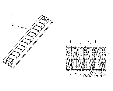
In this example according to Figures 1, 2, 3, 4, 8, 12, 13, 14, 15 to 18 is
described a
structure of the emitter with a ferrite core 1 of rectangular cross-section.
The core 1 has the
length of 9 mm and the cross-section 0,8 mm x 0,6 mm. To the core 1 is
appended a non-
conductive substrate 6, which has the width of 0,8 mm and the thickness of
0,04 mm. On the
core 1 and also across the non-conductive substrate 6 are winded 21 threads 2
of copper
insulated wire placing right next to each other. One thread 2 is made up of
six parallel wires 4
with a diameter of 0,05 mm. This will replace the flat conductor of one thread
2 sized 0,3 mm x
0,05 mm.
On the non-conductive substrate 6, at the ends, are two connecting pads 7, on
which are
conductively linked six wires 41, 42, 43, 44, 45, 46. Wires 41, 42, 43, 44,
45, 46 at the ends of
the core 1, that is after the last thread 2, draw apart to create bigger space
for the tip of an
ultrasonic welder. Wires 41, 42, 43, 44, 45, 46 are ultrasonically bonded
down, welded to the
contacting pads 7.
18
CA 02890584 2015-05-05
WO 2014/076669 PCT/IB2013/060178
At the same time, the connecting pads 7 are linked to a contact, with which is
whole the
emitter's body soldered to the substrate, in this example, to the substrate of
the removable
memory card 5 of microSD format. The emitter on the removable memory card 5 is
located
opposite to the zone with card contacts, in this example, preferably right in
the part where the
card has a small thickening to facilitate easier card removing from the slot
12.
Core 1 with a cross-section of 0,8 mm x 0,6 mm has the equivalent radius of
0,391 mm.
This is the radius at which the circular core has the same area 0,48 mm2 as is
the cross-sectional
area of the rectangular core with parameters of 0,8 mm x 0,6 mm. With 21
threads per length 9
mm, the effective width w of one thread 2 is about 0,428 mm. The ratio between
the equivalent
radius and the effective width is 1 : 1,095, the effective width w of one
thread thus corresponds
to about 1,1 times the equivalent radius.
The advantage of six parallel wires 4, compared to the flat wire is also the
better
conductivity on high frequencies. Due to the skin effect of depth p=17gm/14
MHz the
conductive surface of six circular wires is 7r/2 times greater than in a flat
wire with the same
size, and thus result lower losses. The emitter of this example has at the
frequency of 14,4 MHz
inductance L=1,3 pH and quality Q=21 in power load of 13 dBm.
The antenna array comprises of an antenna energizer (driver), series parallel
resonant
system with the magnetic field emitter and a low noise amplifier with high
profits (limiter).
Driver is designed into bridge connection (H bridge) with output resistance
Rout of less than 4
Ohm at bridge supply voltage Vcc=2,7V. Due to the fact that the switching time
of MOSFET
transistors is less than ins, the higher switching harmonic products need to
be filtered by
capacity C3. Switching signals of bridge H+ and bridge H- are mutually out of
phase by 2,2 ns
so that to prevent simultaneous switching of both controlled branches and thus
a short-circuit of
power supply Vcc to ground.
By the structure described we achieve the effect of the "magnetic gun" with
horizontal
emission at the ends of the ferrite rod of the core 1. The magnetic gun
theory, as defined in this
invention, is in that the magnetic field lines cannot leave the ferrite rod of
the core 1 earlier than
at its ends, and that is because the electrically conductive materials of
wires 4 with closer
mutual winding are impermeable. And since the magnetic field lines must always
be enclosed
in to each other, the only place where they can leave the emitter, are the
ends of the core 1. In
practice, however, it is not possible to make a winding so that there is no
air gap between the
wires 4 and, therefore, part of the field lines penetrate through wires 4.
Excellent emission
characteristics of the emitter, which is placed inside the metal shielding,
are observed in Figure
15.
19
CA 02890584 2015-05-05
WO 2014/076669 PCT/IB2013/060178
The emitter is located inside a mobile phone that has metal covers. This is
visible in
Figure 15 as the shielding cover 3, i.e. the magnetic field flow barrier. The
magnetic field lines
come out from small gaps between covers, i.e. to the area where NFC reader is
placed.
Due to different background location, the emitter detunes, and in the case
that it is
located in close proximity to electrically conductive materials, the emitter
inductance is reduced
to 1[tH. This attribute is used for automatic control of emitted power
depending on the
environment, in which is located. The emitter is tuned to the resonance 15 MHz
only if it is in a
metal housing (environmental impact reduced the antenna inductance to 1 41)
Metal housing
represents the shielding cover 3. However, if placed outside the housing, the
inductance is
increased to 1,3 [tH and the resonance is moved to 12 MHz. Since the emitter
power is emitted
at the frequency of 14,4 MHz, so the maximum power is remitted precisely when
the resonance
is close to that value, as its internal resistance is then the smallest, about
20 Ohm. However, if
the emitter is placed the under plastic cover, resonance is shifted down to 12
MHz and the
internal resistance having the frequency of 14,4 MHz grows to 50 Ohm. Due to
this
configuration we reach a status that the emitter placed under the metal cover
emits the
maximum power, while in a situation when it is under plastic cover, emitted
power
automatically goes down, thereby ensuring that in this case the receiving
devices (POS
terminals) are not energized with too high signal. This automatic attunement
of emitter power
when the impedance varies according to the environment is shown in Figure 18.
Example 2
In this example, as shown in Figure 5 and 6, is used the flat insulated wire
4, the cross-
sectional height of which corresponds approximately to one eighth of the cross-
sectional width
of the wire 4. The flat wire 4 can be used in the oval cross-sections of the
core 1, where at small
sizes and small radius of the rectangular core 1 rounding, there is no risk of
damaging or
breaking the wire 4 in his winding onto the core 1. In another example of
construction, the wire
4 can be created on the core 1 by the vapor deposition of the metal layer, or
other similar
technology of coating a conductive path to the surface. On the core 1, a mask
in the function of
separating gaps between the threads at least equal to the thickness of the
wire 4 can be
created. The mask in this case is in shape of a screw lead strip with a width
forming inter-thread
insulation 8. Then the metal layer is applied to form a flat, wide coil. By
potential application of
insulation on the edge of the wire 4 and then repeatedly applying the
conductive layer strip,
which will overlap the inter-thread gap, can arise the fitting of flat wire 4
edge limiting a
magnetic field leakage out of the core 1 ends.
CA 02890584 2015-05-05
WO 2014/076669 PCT/IB2013/060178
Example 3
In this example, as shown in Figures 5 and 7 is the flat insulated wire 4. led
across the
edge of adjacent thread 2 to form a thread overlap to prevent penetration of
the magnetic field
between the threads. However, still remains the possibility of magnetic field
leakage through a
gap with a thickness that is twice the thickness of insulation 8 of the wire
4.
Example 4
In this example, as shown in Figures 9 and 10 is used a combination of non-
insulated
wires 42, 43, 44, 45, 46 and insulated wires 41 and 47 One thread 2 is made up
of seven wires
4, where the two marginal wires of the given threads 41 and 47 have insulation
8 to avoid inter-
thread short circuit at tight winding. Non-insulated wires 42, 43, 44, 45, 46
are placed inside the
group. As they do not have insulation 8, it will reduce the formation of gaps
for magnetic field
leakage and these wires 42, 43, 44, 45, 46 do not need to be electrically
interconnected.
Therefore, only the wires 41, 42, 46 a 47 are output to the connective pad 7.
Example 5
In this example, according to Figure 11, for creation a single thread 2 is
used a
combination of one flat non-insulated wire 42 and two insulated wires 41, 43
with a classic
circular cross-section. That combination makes production of emitters simple
like the
appropriate, available flat wires with a small thickness do not have any
insulation. Boundary
wires 41 and 43 form inter-thread insulation and are on the connecting pad 7
conductively
linked to each other and also to the flat wire 42.
Example 6
In this example, the core 1 takes the form of a ferrite rod with a circular
cross-section of
the diameter 0,8 mm and the length of 7 mm. The emitter has 17 threads 2, the
effective width
w of the thread 2 is 0,41 mm. The ratio of the effective width of thread 2 to
the radius of the
core 1 is 1,025. The permeability of the core 1 is chosen so that at given
emitter's size and
winding the inductance was L=750 nH.
In this example there is an emitter placed on the removable memory card 5,
which also
contains the payment card function and for the communication between this
payment card and a
POS terminal, a data transmission method that uses two different frequencies
is used. The POS
terminal contains a contactless payment card reader. The cards have to
approach the Operating
volume of the reader in order for the communication connection to be
established. The
placement of the payment card containing a communication element into the
mobile memory
21
CA 02890584 2015-05-05
WO 2014/076669 PCT/IB2013/060178
card 5 into the slot 12 deteriorates the possibility of full approach of the
communication
element on the payment card to the center of the reader's operational volume.
At the same time,
the mobile phone slot 12 is primarily designed for the insertion of a common
memory card 5.
For the communication element, for the slot 12, presents an undesirable
shielding, part of the
slot's 12 body is made of metallic shapes shell. The communication element
contains the
emitter according to this invention, and in this example, it is placed
directly on the micro SD
card. The card's 5 format does not limit the extent of this invention, in the
future any format
whatsoever could be used. The continuing miniaturization of the memory cards 5
and of the
corresponding slots 12 deteriorates the possibilities of effective placement
of the
communication element on the card 5; however the solution described here
solves the problem.
The communication element uses the NFC platform. In real environment and in
case of the
mobile phone is handled in a normal way by the user the transformer connection
coefficient is k
= 0,2 ¨0,001.
The contents and the structure of the transmitted data can be different, in
this example
the data necessary during communication and authorization of payment processes
will be dealt
with. The owner of a mobile phone equips his device with a memory card 5 that
is equipped
with a non-stationary magnetic field emitter. By doing this, he extends the
functionality of his
mobile phone. In preferable configuration, there will be also a payment card,
corresponding to a
different invention of this patent's applicant, on the memory card 5. It is
important, that the
connection of a mobile phone with a memory card 5 will appear to the PUS
terminal and its
payment card reader as a standard contactless card. So the structure of
transmitted data will be
in the accordance with the standards in payments. The advantage of the
solution mentioned is a
comfortable usability of the mobile phone user interface.
The emitter contains a generator of the electromagnetic waves with the
frequency of
14,4075 MHz 7 kHz. This frequency is for 847 kHz higher than the receiver's
frequency. The
receiver's frequency is in the standard 13,56 MHz 7 kHz. The difference
between the
frequencies is 1/16 of the carrier frequency of the receiver. It is important,
if the generator is
connected and active to energize the emitter when data are transmitted over
transformer
connection, which was not used up till now. In case generator existed in the
emitter in already
existing solutions, the generator was not designed for active activity in the
transformer
connection, since it was not necessary due to the same transmitting frequency.
The generator is
connected to the resonant circuit, the output of which is connected to the
antenna.
The data from the emitter on the memory card 5 are transmitted into the
receiver in the
PUS terminal reader through the transformer connection of the emitter and
receiver antenna
inductions M. The data are modulated into the signal on the emitter's side and
the receiver
22
CA 02890584 2015-05-05
WO 2014/076669 PCT/IB2013/060178
transmits the carrier signal. The distance of the emitter from the receiver
will be in cm,
basically, the mobile phone's body will be touching the reader, the
transmission will be
contactless in physical sense. The emitter can even move in the operational
volume, while his
speed would be lower than 1 m/s.
The emitter sends the signal with the frequency 14,4075 MHz 7 kHz, the
receiver's
carrier frequency is 13,56MHz 7kHz. The difference between the frequencies
has a value that
corresponds to the size of the subcarrier frequency, which is derived as a
1/16 of the carrier
frequency according to the ISO 14443.
In antenna arrays of the receiver and the emitter, the signals of different
frequencies are
combined and in the receiver's on the antenna's output, the signal appears in
the form of a
connection of a carrier frequency and modulated subcarrier frequency with
data. The carrier
signal is separated from the result of the signal combination in the receiver.
The result of this
separation is a subcarrier signal, even though the emitter has never
transmitted it physically.
From the subcarrier signal the transmitted data are demodulated. The
demodulation element,
resonance circuit and receiver's generator have the same configuration and
function as in
today's existing technical solutions.
In this example, the basic time unit etu corresponds to the one bit time
interval, so to the
time necessary to transmit one data unit. In the data flow direction from the
emitter into the
receiver, the etu is defined as letu=8/ft, where one ft is a frequency of the
modulated signal that
was transmitted by the emitter. The basic transmission velocity is 106
kbits/s. During
modulation of the signal from the emitter, it is sufficient, if the phase is
changed once per 1 etu
(approx. once per 9,3 [is), so 16 times less frequently in comparison to the
existing load
modulation. Smaller broadband generates 12dB less noise. The data transmitted
are modulated
directly by a change of the emitter's frequency signal phase, where (p=0 or
(p=180 . This
modulated signal could also be called the emitter's carrier signal, since
however the emitter
does not create the subcarrier frequency, then, this frequency is only called
the emitter's signal
frequency.
The emitter is narrowly tuned to the transmitting frequency of 14,4075 MHz, it
has the
narrow and high course of the FFT curve. The emitter is tuned without
considering the emitting
characteristics for the transmission of the subcarrier frequencies 847 kHz. In
case this antenna
should transmit even the subcarrier frequency, the radiation characteristics
would we
insufficient for a reliable transmission. In the solution according to this
invention, it is
important that the signal radiation with the transmitted data is realized
exactly on the 14,4075
MHz frequency, which is the peak of the FFT curve.
23
CA 02890584 2015-05-05
WO 2014/076669 PCT/IB2013/060178
In this example, it is necessary to ensure even reverse data flow direction
from the POS
terminal reader into the memory card 5 in the mobile phone. The emitter
encompasses the
demodulation element, which is connected to the antenna inductance turning
towards the sensor
resistor, preferably over inductor. The usage of the inductor decreases the
voltage peaks on the
entrance to the demodulation element. Thanks to the turning and the inductor,
the demodulation
element can be dimensioned to a smaller voltage. In this data flow direction,
the etu is defined
as 1 etu = 128/fr, where fr is the carrier frequency of the receiver.
Example 7
The ferrite core 1, in a form of ferrite rod with angular cross-section, is
coated by
conductive layer, which forms the wire 4. First, on the core 1 is placed a
screw led mask, which
will separate threads 2 apart. Then, the core 1 is coated by a metal layer
where, due to a
separating mask, is created the coil with desired number of threads 2. The gap
created by a
mask represents the inter-thread insulation. The ending of a coated metal
layer on the sides of
the core 1 form connecting pads 7 which then attach the whole emitter element
to the substrate.
In this example (but it may also be related with other examples), the emitter
is located
on the mobile phone PCB board 10. The telephone has a housing with metal
parts, which
represents shielding covers 3. Thanks to the use of the emitter according to
this invention,
essentially, the emitter can be placed on any free space on the PCB board 10
and there are no
problems with a poor magnetic field penetration out of the mobile phone's
body.
Example 8
The emitter, as shown in Figure 23, is made similar to examples 1 to 7. Mobile
phones
manufacturer designs new models in a way that when designing PCB board 10, is
not limited
by the demands for the known types of NFC antennas. Different types and models
of mobile
phones are equipped with one type of emitter type directly on the PCB board
10.
Example 9
The emitter is located in the SIM card 9. The core 1 of the emitter is in
different
versions according to Figures 19 to 22 oriented and located differently.
Example 10
The emitter as shown in Figure 24 is placed in the body of the mobile phone
battery 11.
Basically, it is a charging accumulator 11, which, however, is commonly called
a battery 11. In
24
CA 02890584 2015-05-05
WO 2014/076669 PCT/IB2013/060178
regard to a small thickness of the core 1, the emitter is placed on the
surface of a common
battery 11 under the last layer of the plastic battery 11 housing.
Example 11
NanoSIM card 9 slot 12, as shown in Figure 26, has a holder of shaped metal
plate. The
slot 12 includes an amplifying element 13 in the form of a ferrite foil.
NanoSIM card 9 has the
emitter on the edge of the card's body of the card.
INDUSTRIAL APPLICABILITY
Industrial applicability is obvious. According to this invention, it is
possible to produce,
by industry and repeatedly, and use non-stationary magnetic field emitters in
the capacity of an
antenna placed directly on the removable memory card with a high emissivity
and small size. A
new type of emitter modulation substantially reduces noise and allows to
increase the magnetic
field intensity in the emitter's core.
LIST OF RELATED SYMBOLS
I- core
2- thread
3- magnetic field flow barrier
4- wire
41, 42, 43, 44, 45, 46, 47 to 4N ¨ wires of one thread / one-thread wires
5- removable memory card
6- non-conductive substrate
7- connecting pad
8- wire insulation
9- SIM card
10- PCB board
11- accumulator / battery
12- slot
13- amplifying element
w ¨ effective width of thread
PCB - printed circuit board RFID ¨ Radio-frequency identification
NFC - near field communication SD - Secure Digital
PUS ¨ point of sale SIM - Subscriber Identity Module