Note: Descriptions are shown in the official language in which they were submitted.
CA 02892528 2015-05-25
WO 2014/149783
PCT/US2014/020911
1
METHOD AND APPARATUS FOR PROVIDING WELDING POWER
FIELD OF THE INVENTION
[00011 The present disclosure relates generally to the art of providing
welding
type power. More specifically, it relates to providing welding type power
using an inverter
based output circuit.
SUBSTITUTE SHEET (RULE 26)
2
BACKGROUND OF THE INVENTION
[0002] There are many known types of welding-type power supplies that
provide welding
type power. Welding type power, as used herein, refers to power suitable for
electric arc welding,
plasma arc cutting or induction heating. Welding-type power supply, as used
herein, refers to a
power supply that can provide welding type power. Welding type systems are
used to perform a
variety of processes and used in a variety of settings. Welding-type system,
as used herein, is a
system that can provide welding type power, and can include control and power
circuity, wire
feeders, and ancillary equipment.
[0003] Some welding type systems include a preregulator which provides
a de bus, followed
by an inverter based output circuit. The preregulator conditions the input
power, and provides a
known de bus. The inverter based output circuit receives the bus and provides
the welding type
power as an output. One successful design includes a boost circuit as part of
the preregulator, and
the output circuit includes an inverter, transformer, rectifier and output
inductor. This type of
welding power supply is described in USP 6987242 (Geissler). Other welding
type power
supplies that have inverter based output circuits include USP 6115273
(Geissler) and Patent
Publication 20090230941 (Vogel), all three of which are owned by the owner of
this patent, and
all three of which may be reviewed for details. Other welding type power
supplies include
additional stages, or use other topologies for each stage (such as a buck
preregulator, a combined
rectifier-boost preregulator, a chopper instead of or following the inverter,
a second inverter
following the first inverter, etc.
[0004] Inverter based output circuits offer many advantages, but they
do have some
drawbacks. First, the switches and diodes used in an inverter circuit can
fail, particularly when
exposed to higher than rated voltages. Clamping voltages are known, but can
result in excess
losses. Also, commutating switches and diodes can create excess heat. USP
6801443 returned
the entire clamp energy back into the output in one single switching event.
CA 2892528 2020-04-28
CA 02892528 2015-05-25
WO 2014/149783
PCT/US2014/020911
3
[0005] Most welding type power supplies include and output inductor.
Starting
the welding process can be difficult, particularly with a large output
inductor, because the
inductor must be "charged" before welding can be preformed. This can be made
more
difficult during starting because of the higher than usual arc voltage, Past
welding type
power supplies have started by a "crowbar" of the bus but that can stress
components.
[0006] Accordingly, a welding type power supply with an inverter
output circuit
that is clamped in an efficient manner is desirable. Preferably, such welding
type power
supply would also provide for efficient commutations of devices and will
provide for
efficient starting of the weld process.
SUBSTITUTE SHEET (RULE 26)
CA 02892528 2015-05-25
WO 2014/149783
PCT/US2014/020911
4
SUMMARY OF THE PRESENT INVENTION
[0007] According to a first aspect of the disclosure a welding type
power supply
includes an input circuit, a controller and an output circuit. The input
circuit receives an
input power signal and provides an intermediate power signal. The output
circuit
receives the intermediate power signal and provides a welding type power
output. The
output circuit has an inverter with at least two inverter switches, and a
clamp circuit that
limits the voltage across the inverter. The clamp circuit captures and buffers
the excess
energy, and returns the excess energy to an input of the inverter over a
plurality of
switching cycles. The controller has control outputs connected to the input
circuit and the
output circuit, to control them.
[0008] According to a second aspect of the disclosure a method of
providing
welding power includes receiving input power and providing an intermediate
power
signal. The intermediate power signal is inverted by controlling at least two
inverter
switches to provide an inverter output. The voltage across the inverter is
clamped and the
excess energy is captured and buffered provided to an input of the inverter
over a
plurality of switching cycles.
[0009] The clamp circuit includes a buck circuit in one embodiment.
[00101 The output circuit includes an intermediate inverter, a
transformer and a
rectifier in another embodiment. The intermediate inverter receives the
intermediate
power signal and provides an intermediate ac signal to the transformer. The
transformer
provides a transformed ac signal to the rectifier. The rectifier provides a
rectified de
signal to the inverter.
[00111 The rectifier includes at least two diodes and a second clamp
circuit limits
the voltage across the at least two diodes, and provides an output across the
voltage
source in another embodiment,
[00121 The clamp circuit includes a voltage source connected to the
buck circuit
in one alternative,
[0013] The inverter is a half bridge inverter with two inverter
switches or a is a
full bridge inverter with four inverter switches in other alternatives.
SUBSTITUTE SHEET (RULE 26)
5
[0014] The buck circuit has a buck switch, and feedback indicative
of the voltage
across the clamp is provided to the controller so that the controller controls
the buck
switch in response to the voltage across the inverter in yet another
embodiment.
[0015] According to a third aspect of the disclosure a welding
type power supply
includes an input circuit, an intermediate inverter, a transformer, a
rectifier an output
inductor and a controller. The input circuit receives an input power signal
and provide an
intermediate power signal. The intermediate inverter receives the intermediate
power
signal and provides an intermediate ac signal. The transformer receives the
intermediate
ac signal and provides a transformed ac signal. The rectifier receives the
intermediate ac signal
and provides a rectified dc signal to the inductor. The rectifier includes at
least
two diodes and a clamp circuit that limits the voltage across diodes and
captures the
excess energy. The controller controls the input circuit and the intermediate
inverter.
[0016] According to a fourth aspect of the disclosure a welding
type power supply
includes an input circuit, an output circuit, and a controller. The output
circuit receives
the intermediate signal and provides a welding-type signal. The output circuit
includes an
output inductor and an inverter. The inverter has at least two inverter
switches. The
inverter includes a clamp circuit having a voltage source and the clamp
circuit is
connected to charge the inductor. The controller controls the input circuit
and the output
circuit.
[0016A] According to a further aspect of the disclosure a welding
type power supply
including an input circuit disposed to receive an input power signal and
provide an
intermediate power signal; an output circuit, disposed to receive the
intermediate power signal
and provide a welding type power output. The output circuit includes an
inverter connected to
receive power from the input circuit and having at least two inverter
switches. The inverter
includes a clamp circuit connected to the inverter that limits the voltage
across the inverter.
The clamp circuit includes at least one switch and an inductor and a capacitor
connected that
capture and buffer the excess energy. The capacitor has sufficient capacitance
to return the
excess energy to an input of the inverter over a plurality of switching
cycles; and a controller
having control outputs connected to the input circuit and the output circuit.
[0016B] According to another aspect of the disclosure a method of
providing welding
power, includes receiving an input power signal and providing an intermediate
power signal;
converting the intermediate power signal to a welding type signal, including
inverting a de signal by
CA 2892528 2017-10-04
5a
signal by controlling at least two inverter switches to provide an inverter
output; and clamping the
voltage across the inverter, the clamp circuit having at least one switch and
an inductor and a
capacitor with sufficient capacitance, is connected for capturing and
buffering the excess energy,
and returning the excess energy to the inverter over a plurality of switching
cycles; and a
controller having control outputs connected to the input circuit and the
output circuit.
[0016C] According to an aspect of the disclosure a welding type system,
including means for
receiving an input power signal and providing an intermediate power signal;
means for inverting
the intermediate power signal, connected to the means for receiving; means for
clamping the
voltage across the means for inverting, capturing and buffering the excess
energy, over more than
one cycle and for returning the excess energy to de signal means over a
plurality of switching
cycles. The means for clamping includes a capacitor, an inductor and a switch
and is connected
to the means for inverting. The capacitor has sufficient capacitance to return
the excess energy to
dc signal means over the plurality of switching cycles.
[0016] The clamp circuit limits the voltage across the inverter, and
includes a buck circuit
that can be used to assist in arc striking and stabilizing.
[0017] The output circuit includes a transformer and a rectifier having
at least two diodes,
and a second clamp circuit limits the voltage across the at least two diodes
and provides an output
across the voltage source in another embodiment.
[0018] The input includes a boost circuit, and the intermediate power
signal is a boosted dc
bus in another embodiment.
[0019] Other principal features and advantages will become apparent to
those skilled in the
art upon review of the following drawings, the detailed description and the
appended claims.
CA 2892528 2020-04-28
CA 02892528 2015-05-25
WO 2014/149783
PCT/1JS2014/020911
6
BRIEF DESCRIPTION OF THE DRAWINGS
[0021] Figure 1 is a diagram of a welding-type system in accordance
with the
preferred embodiment;
[0022] Figure 2 is a full bridge inverter circuit used as an
intermediate inverter;
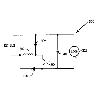
[0023] Figure 3 is a clamp circuit for an inverter;
[0024] Figure 4 is a clamp circuit for an inverter;
[0025] Figure 5 is a diagram of an output circuit; and
[00261 Figure 6 is a full bridge inverter circuit used as an output
inverter.
[0027] Before explaining at least one embodiment in detail it is to be
understood
that the invention is not limited in its application to the details of
construction and the
arrangement of the components set forth in the following description or
illustrated in the
drawings. The invention is capable of other embodiments or of being practiced
or carried
out in various ways. Also, it is to be understood that the phraseology and
terminology
employed herein is for the purpose of description and should not be regarded
as limiting.
Like reference numerals are used to indicate like components.
SUBSTITUTE SHEET (RULE 26)
CA 02892528 2015-05-25
WO 2014/149783
PCT/US2014/020911
7
DETAILED DESCRIPTION OF THE PREFERRED EMBODIMENTS
[0028] While the present disclosure will be illustrated with reference
to a
particular circuit and a particular system, it should be understood at the
outset that other
circuits and systems may be used.
[0029] Generally, the preferred embodiment is implemented with a
welding-type
system such as that shown in US? 6987242. It includes a preregulator input
circuit that
creates an intermediate power signal (preferably a de bus), an output circuit
with an
inverter, a transfoi ____________________________________________ trier, and a
rectifier and a controller. Additionally, an output inverter is
provided in the preferred embodiment, for ac welding. The outrun inverter
receives the
transformed and rectified signal, and provides an ac welding signal. An output
inductor
is provided, preferably after the inverter. Alternatives provide for the
inductor being
before the output inverter, omitting the output inverter, using a chopper,
using a buck
preregulator, using a combined boost-rectifier preregutator, omitting the
boost (and
inverting the rectified input).
[00301 Input circuit, as used herein, includes the circuitry that
receives input
power such as rectifiers, filters, preregulators, etc. Intermediate power
signal, as used
herein, includes the output of the input circuit, and can be a rectified
signal, a regulated
signal such as the output of a boost or buck converter, or an unregulated de
bus. Output
circuit, as used herein, includes the circuitry that provides the welding type
signal, and
can include inverters, converters, transformers, rectifiers, filters, chokes,
etc. Controller,
as used herein, is the digital and/or analog circuitry and/or
logic/instructions that
cooperate to provide control signals to one or more circuits. A controller can
be located
on a single board, or distributed across multiple locations.
[00311 The preferred embodiment has a clamp circuit for the output
inverter, and
a clamp circuit for the output rectifiers. The clamp circuit for the output
inverter includes
a buck converter which takes the energy from clamping and gradually recycles
the excess
energy back into the output circuit (to the input of the output inverter) and
maintains a
controlled stable clamp voltage. The buck circuit also clamps the output
rectifier diodes
and assisting in arc striking and stabilizing by applying the high clamp
voltage to the
output to counter the high arc voltage transient that are encountered. In
other word, the
output of the clamp circuit for the output diodes is fed back to the output
inverter clamp
SUBSTITUTE SHEET (RULE 26)
8
to act as a voltage source. Also, the 300 volt source can be used to quickly
charge the output
inductor.
[0032] Clamp circuit, as used herein, refers to a circuit used to
clamp the voltage across
circuitry to protect that circuitry, such as clamping the voltage across a
diode. Clamp circuit
output, as used herein, refers to the energy that is clamped being provided to
other circuitry.
[0033] Figure 1 is a diagram of a welding-type system 100 in
accordance with the preferred
embodiment. Welding-type system 100 includes an input circuit or preregulator
102, an output
circuit 104 and a controller 106. These modules are preferably designed as
shown in USP
6987242, except as set forth herein.
[0034] Preregulator 102 is preferably a boost preregulator, but other
topologies such as
buck, cuk, etc. may be used. Preregulator 102 preferably provides a 940V
regulated dc bus across
a capacitor 103 to output 104. Other embodiments provide for an unregulated
bus, or for
additional stages as part of input circuit 102, between input circuit 102 and
output circuit 104, or
before or as part of output circuit 104.
[0035] Output circuit 104, shown in more detail in Figure 5,
preferably includes a full
bridge inverter 501, a transformer 503, an output rectifier 505, a full bridge
output inverter 507
and an output inductor 509. Inverters 501 and 507 each include at least four
inverter switches.
Inverter 501 receives the do, bus and inverts it to a desired signal using PWM
at a frequency of
about 20KHz ¨ 40KHz. The frequency is preferably high enough to keep
transformer 503 small.
The load is a primary of transformer 503, and the secondary of transformer 503
is rectified to be a
welding type output. Output inverter 507 inverts the welding type output to
provide an arc
welding output. If dc welding is provided output inverter 507 can be turned
off (or omitted for
only de welding power supplies). Output inverter 507 preferably operates a
welding process
frequency of about 20-400Hz. Alternatives provide that on or both of inverters
501 and 507 be
half bridges, or that other topologies are used. A half bridge inverter
includes at least two
inverter switches. Inverter switch, as used herein, refers to a switch used to
invert a signal. A
single inverter switch maybe comprised of several parallel devices that
function as a single
switch.
CA 2892528 2020-04-28
=
9
[0036] Controller 106 may be discrete components or an integrated
circuit, and it may be
analog or may include a combination of analog and digital control elements.
Controller 106
receives the necessary feedback from preregulator 102 and output circuit 104
to control the
switches in those circuits such that the desired de bus and the desired
welding type output are
provided.
[0037] Figure 2 shows a typical full bridge inverter circuit 200 with
four inverter switches
Si -S4, and four diodes Dl-D4, and capacitors Cl and C2. The load is the
primary of transformer
Ti. The secondary transformer Ti is rectified and provides as the welding-type
output.
[0038] Output circuit 104 also includes a clamp circuit as part of
inverter 507 to limit the
voltage across inverter 507. A clamp circuit 300 is shown in Figure 3 and
includes a buck
inductor 302, a buck switch 304, diodes 306 and 308, capacitor 310 and voltage
source 312. The
output of clamp circuit 300 is provided to the input of inverter 507 (the
output of rectifier 505).
Thus, the energy from clamping is recovered and used in the welding output. As
described
below, the 300 volt source can be recovered from clamping output diodes, it
can be a separate
source, or a combination of independent voltage and recovered voltage.
[0039] The buck converter is also used to assist in arc striking and
stabilizing. The weld
control can override the regular buck converter control (returning energy to
the weld) and have it
apply the higher clamp voltage to the input of the inverter or the rectified
dc link. This allows a
high driving voltage to be applied to the output when needed. Limiting the
voltage across the
inverter, as used herein, refers to clamping the voltage across the diodes in
an inverter bridge.
Voltage across the inverter, as used herein, refers to the voltage across the
diodes in an inverter
bridge.
[0040] Buck switch 304 is controlled to provide three advantages in
the preferred
embodiment. Current (from the output rectifier clamp) is recycled back to the
input of output
inverter 507 in a gradual continuous fashion (i.e., over a plurality of
switching cycles), and
thus the clamped energy is provided back into the weld output in a gradual
fashion, and it
keeps the clamped voltage under control. Also, buck switch 304 is controlled
to aid in revers-
ing the current during commutation of the switches in output inverter 507 by
providing
a high voltage to the output circuit to counter the transient high
CA 2892528 2020-04-28
CA 02892528 2015-05-25
WO 2014/149783
PCT/US2014/020911
arc voltage and keep the current in the output inductor rising. Also, buck
switch 304 is
controlled to provide a high voltage to counter the high initial arc voltage
and help the
current start to rise at the initiation of the weld. The 300 volt source can
be used to
commutate at low current output (when there is neither a need to clamp not
sufficient
energy from clamping to commutate). Buck switch 304 is controlled by
controller 106,
which receives feedback signals indicating bus, clamp and inverter voltages.
300 volt
source 312 is also used in the preferred embodiment to charge output inductor
509 rather
than crowbarring the bus.
[0041] Output circuit 104 includes the secondary of primary 503,
rectifier 505,
including diodes 402 and 404, as shown in Figure 4. A diode 406 clamps diodes
402 and
404, and that clamp is provided as a voltage source 412. This voltage can
override the
300 volt source, or the 300 volt source can be derived from source 412. Figure
6 shows
output inverter 507 in more detail, which includes switches 601-604. Capacitor
310,
diode 306 and output inductor 509 are also shown.
[0042] Alternatives include clamping only output inverter 507 or only
output
diodes 402 and 404, not providing the 300V source, as well as not using the
clamped
voltage to commutate inverter 507, or not using the 300V source to charge
output
inductor 509.
[0043] Numerous modifications may be made to the present disclosure
which still
fall within the intended scope hereof. Thus, it should be apparent that there
has been
provided a method and apparatus for providing welding type power that fully
satisfies the
objectives and advantages set forth above. Although the disclosure has been
described
specific embodiments thereof, it is evident that many alternatives,
modifications and
variations will be apparent to those skilled in the art. Accordingly, the
invention is
intended to embrace all such alternatives, modifications and variations that
fall within the
spirit and broad scope of the appended claims.
SUBSTITUTE SHEET (RULE 26)