Note: Descriptions are shown in the official language in which they were submitted.
CA 02892581 2015-05-26
WO 2014/085562
PCT/US2013/072195
MULTIWAVELENGTH QUANTUM CASCADE LASER VIA
GROWTH OF DIFFERENT ACTIVE AND PASSIVE CORES
CROSS-REFERENCE TO RELATED APPLICATIONS
[0001] This application claims the benefit of priority under 35 U.S.C. 119
of U.S.
Provisional Application Serial No. 61/732,289 filed on November 30, 2012, the
content of which is relied upon and incorporated herein by reference in its
entirety.
FIELD
[0002] The present specification generally relates to semiconductor-based
lasers and,
more specifically, to semiconductor-based lasers particularly for applications
such as
gas sensing, medical diagnostics, and other applications in which a
multiplicity of
different wavelengths or wide-range wavelength tuning is needed. Methods of
making
such devices are also disclosed.
TECHNICAL BACKGROUND
[0003] Generation of multiple wavelengths in the mid infra-red (MIR) from a
quantum cascade lasers has been realized by designing one single core capable
of
emitting two wavelengths simultaneously (see "Bidirectional semiconductor
laser", C.
Gmachl et al, Nature 387, 777 (1999): one core designed such that opposite
bias leads
to emission of two different wavelengths), or by adding gratings with
different
periods to one single core with broad enough gain bandwidth. See, e.g., "High-
performance, homogeneous broad-gain QCLs based on dual-upper-state design", K.
Fujita et al, Appl Phys Lett 96, 241107 (2010) and further work by the same
group in
Appl Phys Lett 98, 231102 (2011): one core which has a wide gain bandwidth and
can
be tuned to emit over a wide range of wavelengths (tuning range 330cm-1 in the
first
work, 600cm-1 in the second). See also "Broadband Distributed-Feedback Quantum
Cascade Laser Array Operating From 8.0 to 9.8 Jim", B. G. Lee et al: one broad-
gain
core, array of parallel devices whose exact wavelength is controlled by a
grating. In
these cases, the wavelength coverage is only about 15-20% of the center
wavelength.
[0004] Another technique consists in stacking different cores on top of one
another,
each emitting at a different wavelength. See C. Gmachl, D. L. Sivco, R.
Colombelli,
F. Capasso and A. Y. Cho, "Ultra-broadband semiconductor laser," Nature, 415,
883-
887, (2002) and C. Gmachl, D. L. Sivco, J. N., Baillargeon, A. L. Hutchinson,
F.
-1-
CA 02892581 2015-05-26
WO 2014/085562
PCT/US2013/072195
Capasso and A. Y. Cho, "Quantum cascade lasers with a heterogeneous cascade:
two-
wavelength operation," Appl. Phys. Lett., vol. 79, 572-574, 2001. Here again,
gratings of different periods can be added above the core to select precise
wavelengths, this time within a somewhat wider range due to the different
cores (30-
40% of the center wavelength).
SUMMARY
[0005] According to one aspect, of the present disclosure, a method of forming
a laser
source capable of producing mid-IR laser radiation comprises growing a first
core
structure on a substrate, etching away the first core structure in one or more
locations,
and growing a second core structure on the substrate. At least one of the core
structures comprises a quantum cascade gain medium emitting at a frequency
within
the range from 3-14 Jim.
[0006] According to another aspect, a laser source capable of producing mid-IR
laser
radiation comprises a quantum-cascade core positioned on a substrate for
emitting
within the range from 3-14 lam and a second core on the substrate positioned
in-plane
relative to the first core. The second core is one of a) a passive waveguide
core b) a
second quantum-cascade core structured for emitting at a frequency differing
from
that of the first core and c) a semiconductor active core region.
[0007] These and other features and advantages will be apparent from the
specification and the drawings to those of skill in the art.
BRIEF DESCRIPTION OF DRAWINGS
[0008] Figs. lA and 1B: Plan and cross-sectional schematic view of one
embodiment
of a multicore device according to the present disclosure.
[0009] Fig. 2: Schematic of certain process steps in a method according to one
embodiment of the present disclosure.
[0010] Figs. 3A and 3B: Plan and cross-sectional schematic view of one
alternative
embodiment of a multicore device according to the present disclosure.
[0011] Figure 4. Schematic cross-sectional view of one alternative aspect of
certain
embodiments of a device according to the present disclosure.
[0012] Figure 5. Schematic cross-sectional view of another alternative aspect
of
certain embodiments of a device according to the present disclosure.
-2-
CA 02892581 2015-05-26
WO 2014/085562
PCT/US2013/072195
DETAILED DESCRIPTION
[0013] The present invention can be understood more readily by reference to
the
following detailed description, drawings, examples, and claims, and their
previous
and following description. However, before the present compositions, articles,
devices, and methods are disclosed and described, it is to be understood that
this
invention is not limited to the specific compositions, articles, devices, and
methods
disclosed unless otherwise specified, as such can, of course, vary. It is also
to be
understood that the terminology used herein is for the purpose of describing
particular
aspects only and is not intended to be limiting.
[0014] The following description of the invention is provided as an enabling
teaching
of the invention in its currently known embodiments. To this end, those
skilled in the
relevant art will recognize and appreciate that many changes can be made to
the
various aspects of the invention described herein, while still obtaining the
beneficial
results of the present invention. It will also be apparent that some of the
desired
benefits of the present invention can be obtained by selecting some of the
features of
the present invention without utilizing other features. Accordingly, those who
work in
the art will recognize that many modifications and adaptations to the present
invention
are possible and can even be desirable in certain circumstances and are a part
of the
present invention. Thus, the following description is provided as illustrative
of the
principles of the present invention and not in limitation thereof
[0015] Disclosed are materials, compounds, compositions, and components that
can
be used for, can be used in conjunction with, can be used in preparation for,
or are
embodiments of the disclosed method and compositions. These and other
materials
are disclosed herein, and it is understood that when combinations, subsets,
interactions, groups, etc. of these materials are disclosed that while
specific reference
of each various individual and collective combinations and permutation of
these
compounds may not be explicitly disclosed, each is specifically contemplated
and
described herein. Thus, if a class of substituents A, B, and C are disclosed
as well as a
class of substituents D, E, and F, and an example of a combination embodiment,
A-D
is disclosed, then each is individually and collectively contemplated. Thus,
in this
example, each of the combinations A-E, A-F, B-D, B-E, B-F, C-D, C-E, and C-F
are
specifically contemplated and should be considered disclosed from disclosure
of A, B,
and/or C; D, E, and/or F; and the example combination A-D. Likewise, any
subset or
combination of these is also specifically contemplated and disclosed. Thus,
for
-3-
CA 02892581 2015-05-26
WO 2014/085562
PCT/US2013/072195
example, the sub-group of A-E, B-F, and C-E are specifically contemplated and
should be considered disclosed from disclosure of A, B, and/or C; D, E, and/or
F; and
the example combination A-D. This concept applies to all aspects of this
disclosure
including, but not limited to any components of the compositions and steps in
methods of making and using the disclosed compositions. Thus, if there are a
variety
of additional steps that can be performed it is understood that each of these
additional
steps can be performed with any specific embodiment or combination of
embodiments of the disclosed methods, and that each such combination is
specifically
contemplated and should be considered disclosed.
[0016] In this specification and in the claims which follow, reference will be
made to
a number of terms which shall be defined to have the following meanings:
[0017] "Include," "includes," or like terms means encompassing but not limited
to,
that is, inclusive and not exclusive.
[0018] The term "about" references all terms in the range unless otherwise
stated.
For example, about 1, 2, or 3 is equivalent to about 1, about 2, or about 3,
and further
comprises from about 1-3, from about 1-2, and from about 2-3. Specific and
preferred values disclosed for compositions, components, ingredients,
additives, and
like aspects, and ranges thereof, are for illustration only; they do not
exclude other
defined values or other values within defined ranges. The compositions and
methods
of the disclosure include those having any value or any combination of the
values,
specific values, more specific values, and preferred values described herein.
[0019] The indefinite article "a" or "an" and its corresponding definite
article "the" as
used herein means at least one, or one or more, unless specified otherwise.
[0020] As used herein, a "superlattice" comprises at least two semiconductor
materials with different bandgaps that produce quantum well confinement and
interband or typically generally intersubband transitions (see, e.g. ,U.S.
Appl. No.
13/661,559, herein incorporated by reference in its entirety). The thicknesses
of the at
least two semiconductor materials may change within lattice or may be of
constant
thickness. If the thicknesses of the materials change, they may change in a
linear or
nonlinear fashion.
[0021] As used herein, a "stage" comprises a series of quantum wells formed by
the
superlattice that allow electrons to transition from an injector region to an
active
section, with the active section structured to induce lasing via one or more
intersubband transitions. A particular stage structure generally lases within
a quite
-4-
CA 02892581 2015-05-26
WO 2014/085562
PCT/US2013/072195
narrow wavelength range. A stack comprises multiple stages arranged in a
stacked
configuration. As used herein, "heterogeneous quantum cascade" comprises a
stack
of multiple stages wherein the stages are not identical, that is, wherein
there are at
least two different stage structures each inducing lasing at differing center
frequencies. The "active region" or "core" is comprised of at least one stack
and is
used to describe the region of the laser that produces the light emission.
[0022] At present, in order to increase the mid-IR optical gain bandwidth
beyond that
of a typical single quantum cascade core, multiple differing stages stacked in
the
growth direction, are proposed and demonstrated. A significant drawback of
this
approach is that the lasing efficiency at a given wavelength is low because
only a part
of the total stack contributes to the lasing.
[0023] As a method to overcome this barrier, a process is disclosed herein for
forming
multiple differing cores in the lateral direction, that is, multiple differing
cores, in-
plane relative to one another, within one wafer. Devices are also disclosed. A
schematic depiction of one such device having such cores is shown in Figs. lA
and
1B, while some steps of such a method are shown in Fig. 2.
[0024] Fig. lA is a schematic top or plan view looking down on a wafer 10 or
laser
source 100 as formed on wafer 10, from the top after the growth of three cores
40, 50,
60. Respective waveguides 70 are associated with each core. The respective
cores are
labeled ),1, ),2, and )3, to indicate that each is structured for generating a
respective
differing emission profile having respective differing center frequencies ),1,
),2, and
a Fig. 2A is a schematic cross section of the structure of Fig. 1A, taken
along A-A
as indicated in Fig. 1A, showing the cores 40, 50, 60 on a substrate and lower
cladding layer 12, with an upper cladding layer 14 above each core. A
conductive
layerl 6 compatible with metallization may lie above the cladding layer, with
respective metal contacts 18 formed thereon for current injection into the
respective
cores 40, 50, 60. At least one of the cores 40, 50 or 60, and in one
alternative
embodiment, two or all three of the cores 40, 50 and 60, are quantum-cascade
type
cores structured so as to produce center frequencies within the range from 3-
14 Jim. In
another alternative embodiment, in addition to at least one core 40 of quantum-
cascade type and structured so as to produce as center frequency within the
range
from 3-14 lam, at least one of the other cores 50 or 60 is in the form of a
semiconductor active core region structured for generating interband
transitions
-5-
CA 02892581 2015-05-26
WO 2014/085562
PCT/US2013/072195
emitting at a center frequency outside the range from 3-14 pm. Thus widely
spaced
wavelength sources may be integrated on the same substrate 12.
[0025] Fig. 2 shows a schematic illustration of certain process steps 20, 22,
24, 26,
28, and 30 according to one embodiment of a method of the present disclosure.
As
illustrated in Fig. 2, in a step 20, a first core structure 40 is grown and/or
deposited
(including by combinations of growth and deposition) on a substrate 12. In a
step 22,
the first core structure 40 is etched away in one or more location on the
substrate,
leaving at least one first core 40 as shown. In step 24, a second core
structure 50 is
grown and/or deposited on the substrate, and in step 26, the second core
structure 50
is likewise etched away in one or more second locations on the substrate,
leaving at
least one second core 50 as shown. These steps may optionally be repeated
further,
with a third core structure 60 as shown in steps 28 and 30 deposited and then
removed
at one or more locations, leaving at least one third core 30 as shown. Each
respective
etch step may desirably take the form of a wet etch, although other suitable
etch
processes may be used. Each respective etch step may be used to remove all of
the
core structure overlying any previously deposited core, or, more preferably,
if butt
joints are to be used, a small overlying portion may be left, as will be
explained
below.
[0026] Because each core 40, 50, 60 is formed separately, this process allows
the
design of each core (both its material and structure) to be optimized to give
high
lasing efficiency and/or power at an assigned lasing wavelength. In
embodiments,
each of the assigned wavelengths are in the mid-IR wavelength region, and each
core
structure is in the form of a quantum cascade gain medium. Desirably, the
width W
of each core is chosen so that the corresponding laser frequency will lase in
single
lateral mode. As shown in the embodiment as shown in Figs. lA and 1B, the
devices
are desirably isolated from one another laterally by side regrowth of barrier
layers 80,
such as of InP layers, which both limits unwanted electrical current injection
and
provides optical confinement. Alternatively, deep-etched trenches (not shown)
may be
used for isolation in the lateral direction.
[0027] In the embodiment of Figs. lA and 1B, the multiple cores are positioned
adjacent each other, side-by-side as part of separate respective waveguides
70. Figs.
3A and 3B show another aspect in which multiple cores 40, 50, 60 are
positioned
adjacent each other end-to-end as part of common waveguides 70, desirably
joined
directly in respective butt-joints J. Fig. 3A is a schematic plan view similar
to that of
-6-
CA 02892581 2015-05-26
WO 2014/085562
PCT/US2013/072195
Fig. 1A, while Fig. 3B is a schematic cross-section of the structure of Fig.
3A, taken
along the line B-B indicated in Figure 3A. The multiple cores 40, 50, 60 of
this
embodiment (three different cores in this instance) each compose part of each
active
device or waveguide, which will thus each emit, at the same time, one, two, or
three
wavelengths ),1, ),2, and )3, depending on how each core is biased (how the
metal
contacts are supplied with voltage/current) at the time in question. The
device of Figs.
3A and 3B may desirably be laterally confined (not shown) in a manner similar
to that
shown in Fig. 1B above.
[0028] Desirably one of the cores 40 is a quantum-cascade core structured for
generating intersubband transitions emitting at a first center frequency
within the
range from 3-14 lam, and a second core 50 (or 60) is one of a) a passive
waveguide
core structured to guide wavelengths having said first center frequency, b) a
second
quantum-cascade core structured for generating intersubband transitions
emitting at a
second center frequency within the range from 3-14 pm different from said
first
center frequency, and c) a semiconductor active core region structured for
generating
interband transitions emitting at a second center frequency outside the range
from 3-
14 pm. The third core 60 (or 50) may further desirably be a quantum-cascade
core
structured for generating intersubband transitions emitting at a third center
frequency
within the range from 3-14 Jim, different from said first center frequency and
(if used)
said second center frequency. Alternatively, the third core 60 (or50) may be a
passive
waveguide core structured to guide wavelengths having said first and (if used)
said
second center frequencies. Such a third core is desirably positioned and
arranged to
form a waveguide multiplexer for the first (and alternatively also the second)
waveguides.
[0029] As another alternative aspect, one (or more than one, should that ever
be
desirable) of the multiple cores 40, 50, 60 can be a passive core structured
to be
transparent to wavelengths emitted by one or more of the other cores, such as
by a
quantum cascade gain medium of one or more of the other cores. Candidate
materials
to form a low optical loss waveguide at mid-IR wavelength include AlInAs,
InGaAs,
GaInAsP, and AlGaInAs. The passive waveguides thus created can be arranged to
serve as splitters or combiners, or multiplexers or demultiplexers to divide
or combine
light, in the form of one-to-many or many-to-one waveguide structures.
[0030] Where butt joints are employed, to ensure a smooth transition between
the
butt-joined cores, the second and any succeeding core growth steps are
preferably
-7-
CA 02892581 2015-05-26
WO 2014/085562
PCT/US2013/072195
performed with at least some portion of the previous core structure (with
which a butt
joint is to be formed) exposed¨that is, with no mask layer or at least without
a mask
layer that covers every part of the top surface area of the previously
patterned core(s).
Substantially all the second or other succeeding core structure may then be
removed
from on top of the first core structure, such as by etching. Alternatively,
and more
desirably, a small portion P of the overlying second or other succeeding core
structure
may be allowed to remain to help ensure and preserve a robust butt joint.
There
desirably should be a small overlapped region (2-10 lam) to have good
fabrication
yield and negligible optical transition loss. Embodiments comprising such
small
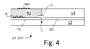
portion P of overlapping core material are shown in figures 4 and 5.
[0031] Figure 4 shows a schematic cross-sectional elevation of a low loss
passive
quantum waveguide core PQ, desirably formed with GaInAsP, butt-joined with an
active gain quantum cascade core QC, with a small overlap of the quantum
cascade
core over the passive core PQ to help ensure and preserve a robust butt joint.
(It
should be noted that the order of core growth need not be as implied by this
structure¨the passive core may be the second or other subsequently grown core,
and
the active core may be the second or other subsequently grown core.) As
another
alternative aspect, gratings G may be added above or below the passive core PQ
to
provide wavelength selective feedback. As a further alternative, one or more
microheaters MH may be added on the top of an electrically insulating top
cladding
layer 90, such as SI-InP, to allow the microheater to selectively change the
refractive
index of the waveguide for wavelength tuning.
[0032] Across all embodiments, cladding layers are provided on both sides of
the
cores in the growth direction, with the bottom cladding layer desirably being
n-doped,
while the top cladding layer is n-doped where current injection is needed, but
is semi-
insulating wherever microheaters are positioned, if any, such as by being Fe-
doped
wherever microheaters are positioned, for example.
[0033] As another alternative aspect, a tunnel junction TJ can be added above
or
below the passive core, as shown (above in this instance) in the schematic
cross
section of Fig. 5, to inject minority carriers for changing the refractive
index by the
free carrier effect.
[0034] Methods of manufacturing may comprise using fabrication processes
similar
to those traditionally used in DFB QCLs. Embodiments herein are advantageous
in
that they can functionally replace tunable EC QCLs with a device having
smaller size,
-8-
CA 02892581 2015-05-26
WO 2014/085562
PCT/US2013/072195
faster speed and lower cost. Further, embodiments also have size and cost
advantages
over DFB QCL arrays, since DFB QCL arrays typically need combining optics to
optically combine the output of an array into one optical beam.
[0035] Embodiments may comprise a gain material comprising at least two,
compositionally non-identical, layers forming a superlattice. By proper design
of the
layer thicknesses, it is possible to engineer a population inversion between
two
subbands in the system which is necessary to achieve laser emission. The
thickness of
the layers may be identical or may be different depending on the desired
design. In
some embodiments, the layers have a thickness from about 1 A to about 500 A.
In
some embodiments, the layers have a thickness from about 10 A to about 100 A.
In
some embodiments, the layers have a thickness of about 1, 2, 3, 4, 5, 6, 7, 8,
9, 10, 11,
12, 13, 14, 15, 16, 17, 18, 19, 20, 21, 22, 23, 24, 25, 26, 27, 28, 29, 30,
35, 40, 45, 50,
55, 60, 70, 80, 90, 100, 125, 150, 175, 200, 250, 300, 350, 400, 450, or 500
A.
[0036] Materials that may be used to form the layers in the gain material
generally
comprise semiconductors, such as group IV, III-V, and II-VI semiconductors. In
some embodiments, the layers may comprise GaAs, AlxGai_xAs, SixGei_x, or
GaxIni_
As and AlyIni_yAs, wherein x and y are from 0 to 1.
[0037] The superlattice gain material may be produced using various
techniques, for
example molecular-beam epitaxy (MBE) (including gas-source MBE and MO-MBE),
metalorganic vapor phase epitaxy (MOVPE), or sputtering. These methods allow
production of layers with thicknesses of only a few atomic spacings.
[0038] Embodiments may further comprise an optical waveguide. An optical
waveguide, as used herein, comprises a physical structure that guides
electromagnetic
waves in the optical spectrum. While not limited to any specific type of
waveguide,
one type of optical waveguide commonly used is a ridge waveguide. A ridge
waveguide is created by etching parallel trenches in the quantum cascade gain
material to create an isolated stripe of QC material, typically, but not
necessarily,
about 5-15 Jim wide and several mm long (the length is usually defined by
cleaving).
Lateral mode confinement may be achieved by the deposition in the trenches of
a
dielectric material, and then the entire ridge is typically coated with gold
to provide
electrical contact and to help remove heat from the ridge when it is producing
light.
More commonly, lateral mode confinement is achieved by growing in the trenches
a
semi-insulating material such as InP if the laser was grown on InP substrate.
Light is
emitted from the cleaved ends of the waveguide.
-9-
CA 02892581 2015-05-26
WO 2014/085562
PCT/US2013/072195
[0039] Embodiments may further comprise an antireflection or antireflective
(AR)
layer. As used herein an AR layer comprises an optical coating applied to at
least one
end (facet) of the device and that reduces reflection, particularly in the IR
region. The
AR layers may be of any type, such as index-matching, single layer
interference,
multi-layer interference, or moth eye (nanostructured). In some embodiments,
the AR
coatings provide less than about 10%, 5%, 4%, 3%, 2%, 1%, 0.5%, 0.1%, 0.01%,
0.001%, or 0% loss.
[0040] Gratings can be patterned by electron beam ("e-beam") writing, contact
printing of a grating mask, manufactured by e-beam lithography, or holography.
[0041] Additional components that may be found in embodiments comprise n-type
cladding layers both above and/or below the gain material. The active gain and
wavelength selective sections may be capped with a patterned electrical
contact layer
which comprises respective control electrodes dedicated to the different laser
sections.
An insulating dielectric material may be deposited in appropriate regions in
the
patterned electrical contact layer to isolate electrically the distinct
regions of the laser
structure.
[0042] In typical embodiments, the lasing sections are separated by a p-type
electrical
isolation region, as described in U.S. Appl. No. 13/050,026, incorporated by
reference
herein in its entirety. For example, an active waveguide core may be
sandwiched
between upper and lower n-type cladding layers. The active core and the lower
n-type
cladding layer, as well as at least part of the upper cladding layer, extend
through the
electrically isolated laser sections of the embodiment. A portion or portions
of the
upper n-type cladding layer comprise sufficient p-type dopant to define p-type
electrical isolation region(s), which extend across part of the thickness of
the upper n-
type cladding layer along a projection separating the sections of the
embodiment. The
upper and lower n-type cladding layers may comprise InP, GaAs, AlGaAs, or any
other conventional or yet-to-be developed cladding material suitable. For
example,
and not by way of limitation, it is contemplated that a variety of cladding
materials
might be suitable, including II-VI semiconductors, Si-Ge or GaN-based
materials, etc.
[0043] There are diverse ways of realizing the p-type isolation regions. Among
these
are selective growth, ion implantation, and diffusion of a p-type dopant. If
the last
option is chosen, the respective compositions of the upper and lower n-type
cladding
layers and the gain material may be selected to facilitate formation of the p-
type
electrical isolation regions by dopant diffusion. More specifically, the upper
and
-10-
CA 02892581 2015-05-26
WO 2014/085562
PCT/US2013/072195
lower n-type cladding layers may comprise InP and the p-type dopant may be
selected
such that its maximum stable concentration in the InP upper n-type cladding
layer is
below approximately n x 1018 cm-3, where n is less than 3.
[0044] An alternative method of isolating the lasing sections comprises
removal of
the highly doped part of the n-cladding layer.
[0045] By way of example, and not limitation, it is alternatively contemplated
that the
upper and lower n-type cladding layers may be GaAs-based cladding layers. Some
of
the cladding layers may be AlGaAs or (A1)GaInP instead of simply GaAs or InP.
For
GaAs-based cladding layers, the core may be GaAs/AlGaAs, AlGaAs/AlGaAs,
(A1)GaInP/(A1)GaInP, or GaInAs/(A1)GaAs. Additional layers of similar
composition
are contemplated for the remaining layers of the structure and should be
selected to
compensate for any lattice-mismatch between GaInAs and the GaAs substrate. For
example, and not by way of limitation, other possible layers are GaInP,
AlGaInP,
GaAsP, and GaInAsP. For GaAs-based cladding layers, suitable dopants used to
make (A1)GaAs semi-insulating include, but are not limited to Cr and 0. At
very low
temperature growth, semi-insulating (A1)GaAs can be obtained without any
dopant.
[0046] Embodiments herein are desirably used in a pulsed mode, but continuous-
wave mode may be useful in some applications. Laser pulse duration may be from
about 1 ns to about 1 ms. In some embodiments, the pulse width at FWHM is
about 1
ns, 2 ns, 3 ns, 4 ns, 5 ns, 6 ns, 7 ns, 8 ns, 9 ns, 10 ns, 20 ns, 50 ns, 60
ns, 70 ns, 80 ns,
90 ns, 100 ns, 200 ns, 300 ns, 400 ns, 500 ns, 600 ns, 700 ns, 800 ns, 900 ns,
1 [Ls, 10
[Ls, 100 [Ls, or 1 ms. In some embodiments, devices embodied herein may be
designed to fire all laser sections simultaneously, individually, and/or in a
sequential
or programmed order.
[0047] Embodiments may be used in any number of methods wherein IR radiation,
and particular IR laser radiation would be advantageous. Particular
applications
include IR absorbance or reflectance measurements, IR and FTIR spectroscopies,
Raman spectroscopy, gas and/or chemical weapons detection, chemical dynamics
and
kinetics measurements, thermal experiments, etc. In one embodiment, the
embodiments are used in IR absorbance measurements to identify molecular
compositions.
-11-