Note: Descriptions are shown in the official language in which they were submitted.
CA 02892684 2015-05-26
1
SWITCHABLE DIRECTIONAL INFRARED RADIATION SOURCE
The field of the invention is that of directional sources of infrared
radiation.
The blackbody concept serves as a model for the far field emissive
behavior of hot bodies. It will be recalled that according to Wien's law, the
wavelength Aw of which a blackbody emits the most radiant light flux, which
flux is here denoted 1, is inversely proportional to temperature T (expressed
in K): Aw = 2898 (in pm K)Ir .
In the natural state, the far field emissive behavior of a solid hot
body is most often very similar to that of a blackbody. Its emission is
incoherent, i.e. it is isotropic (Lambertian) overall, and of broad spectral
width.
Emissivity e(A, 0) relates the emission spectrum 1(A, 0) of a hot
body at a wavelength A in the direction 9 to the emission of a blackbody lo,
and is defined by the ratio:
e(A, 8)= 1(A, 0)/lo(A,T)
lo(A,T) being the monochromatic radiant flux of a blackbody of temperature T
at the wavelength A and 1(A, 0) that of the object at the same wavelength in
the direction 0.
Control of the emission direction is associated with the spatial
coherence of the electromagnetic field. The longer the correlation length, the
greater the directivity. Under these conditions, thermal sources may behave
as veritable antennae. To date, many directional thermal sources have been
designed by structuring materials at subwavelength scales.
- In 1999 Carminati et al., then Shchegrov et al. (2000) demonstrated that the
field associated with a resonant surface mode possesses a high spatial
coherence. However, as this field remains confined to the vicinity of the
interface, far field thermal emission remains incoherent.
- In 2002, Greffet et al. (Greffet et al., 2002) demonstrated that it was
possible to export the spatial coherence of these waves to the far field using
a surface grating. The structure of such a source 100' is shown in figure 1:
it
consists of a bulk sample 50' of SiC, the surface of which has been etched to
CA 02892684 2015-05-26
2
form a 1D grating. However, one of the weaknesses of this type of source
resides in the drift in the emission direction with wavelength. In addition, a
high directivity is observed only for the p polarization, the only
polarization to
which the resonant surface mode couples, the electric field of this
polarization having no component along the surface. Thus, for the s
polarization the radiation emitted remains incoherent.
- To mitigate this drawback, Kollyukh et al. (2003), Ben-Abdallah (2004)
and
Celanovic et al. (2005) proposed to use single films or microcavities to
exploit
the presence of Fabry-Perot type guided modes and cavity modes to control
the emission pattern simultaneously for both polarization states. Veritable
thermal antennae, these structures nevertheless exhibit a low emissivity
level.
- Other more complex structures have been proposed to improve the degree
of coherence of these sources. This is the case for the structures proposed
by Lee etal. (2005). These sources, composed of a periodic one-dimensional
multilayer structure (1D stack) coupled to a polar material, allow the
direction
and frequency of emission to be controlled simultaneously for both the s and
p polarization states of light. However, the directional control of the
emission
of this type of planar source remains low.
- To mitigate this problem, hybrid structures that associate a number of the
features of the structures described above have been developed (Drevillon et
al. 2007). Among these structures, mention may be made of that proposed
by Battula & Chen (2006). It is here a question of nanostructured multilayer
materials composed of a cavity placed between a surface grating and a 1D
photonic crystal, i.e. a 1D surface grating. This structure allowed a source
having a high spatial but also temporal coherence in the visible and near IR
to be obtained. The long coherence length of this structure is attributed on
the one hand to the excitation of evanescent waves on the surface of the
grating. On the other hand, the photonic crystal acts as a polarizer and
suppresses the emission of nonresonant s-polarized radiation that would not
be directional, leaving the emissivity high only for the resonant component of
the emission. Lastly, the high degree of temporal coherence (therefore the
small width) is due to the presence of the cavity that surmounts the photonic
crystal and that amplifies the emission at the frequency of the resonant
modes.
CA 02892684 2015-05-26
3
- Joulain & Loizeau (2007) have also demonstrated that it would be possible
to obtain a temporally coherent directional thermal source by coupling a
surface grating to a simple guide. However, this work relied on a theoretical
approach and was limited to one-dimensional gratings.
- It has also been envisioned to use metamaterials, artificial composite
structures that exhibit a negative dielectric permittivity and a negative
magnetic permeability, to control the direction of thermal emissions (Enoch,
2002). However, the absence of natural magnetic resonance in the infrared
and difficulties with fabrication have slowed the development of these
materials.
- However, in 2005 a team of researchers (Zhang et al., 2005) demonstrated
that it would be possible to design 3D metamaterials in the near infrared (2
pm) by combining perforated dielectric structures and metal films. An
analogous result was also obtained in the far infrared (40 to 60 pm) using
composite structures based on gold wire (Wang et al., 2007). In contrast to
the structures proposed by Zhang et al. (2005), the optical behavior of which
was based on a complex set of interferences between electromagnetic
waves in these structures, it is the presence of stationary waves along the
wires that allows a negative refractive index to be produced, including for
the
"s" polarization.
These various thermal sources are not switchable insofar as only
a mechanical solution, such as a shutter for example, allows the emission of
the entirety of the spectrum to be suppressed (or practically suppressed).
The position of the emissions may also be shifted over the spectrum by
changing the temperature of the source until the Wien wavelength Aw departs
so far from the range of interest that the emission weakens, this approach
moreover having a high inertia. However, the emission mechanism is in no
way suppressed.
Moreover, one solution commonly implemented to obtain a
directional thermal source that is directionally modulable in its emission
band
consists in associating:
- a weakly directional IR radiation source such as a wire, filament or
strip; and
- a mechanical device allowing the radiation to be concentrated in a
privileged direction, such as a parabolic or paraboloidal reflective
CA 02892684 2015-05-26
4
surface for example, and the orientation of which may be varied. The
use of glass optics is generally precluded in the mid-infrared and
optics made of alternative materials (ZnSe, Ge, CsI) suitable for these
wavelengths are expensive and fragile.
The switching (turning on/off) and modulation (change of the
emission direction) functionalities obtained in this way have drawbacks in
terms of inertia, when one operating state is changed to another, and also in
terms of bulk: the optics (the reflective surface) must be much larger than
the
actual source in order to obtain sufficient directionality.
In summary, there exist directional thermal sources that are not
switchable and switchable sources that are not modulable without external
devices (shutters, reflectors) and that are moreover rather slow to switch.
Therefore, there remains to this day a need for a non-wire source
of infrared radiation that simultaneously meets all of the aforementioned
requirements, especially in terms of providing a satisfactory far-field
emission
level, in terms of directional control of the emissivity, in terms of ease of
fabrication, in terms of switching in its emission band, and in terms of low
bulk. The field of application where this need is present is notably that of
infrared spectroscopy, but also that of heating in any context where a form of
agility is required (food-processing, health, control of chemical processes,
individual heating of a seated or standing individual, etc.).
The subject of the invention is a directional thermal source
comprising a substrate bearing an external layer especially made of a metal
insulator transition (MIT) material that possesses a crystalline phase and an
amorphous phase that is in general the high-temperature phase. It operates
in two different configurations:
non-emitting source (emissivity very low relative to that of a
blackbody) when the material of the external layer is in its crystalline
state; and
high-emissivity directional source with an emission similar to that
of a blackbody at the same temperature as the source, when the
CA 02892684 2015-05-26
external layer is in a hybrid crystalline/amorphous state that then
forms a diffraction grating.
The switch from one configuration to another occurs reversibly at
the critical transition temperature Tc of the MIT material, the wavelength Ac
5 corresponding to this temperature Tc being in the emission range of the
source; this switching is achieved electrically under the action of an
optionally
pulsed electrical current or indeed thermally under the action of heat sources
arranged so as to define a field of variable temperature.
If necessary, an insulating layer prevents phase transitions in the
MIT material in other regions of the source, especially those under the
surface of the external layer.
More precisely, the subject of the invention is a source of
directional radiation in an IR band, mainly characterized in that it comprises
at least:
a substrate; and
an external layer comprising controllable cells made of a metal
insulator transition material that changes phase at a temperature Tc at
which the corresponding wavelength is located in the IR band and that
possesses a crystalline phase and an amorphous phase; and
control means for controlling the phase change of the controllable
cells so as to form in this external layer a diffraction grating when the
cells are controlled to the amorphous phase
Thus, a directional source that is switchable depending on its
temperature relative to Tc is obtained. Thus, by varying the temperature only
for a thin exterior film, and for a minimal change in temperature, the same
effect as that obtained by switching the thermal power provided to the source
on/off is obtained. It is thus advantageously possible to obtain a switchable
infrared source.
The diffraction grating is advantageously periodic.
According to one feature of the invention, the control means are
electrical and optionally comprise a generator of electrical pulses.
The control means may be able to control groups of cells, each
group comprising a variable number of cells.
Preferably, the source comprises means for supervising the
control means, which means are configured to modify the spatial
CA 02892684 2015-05-26
6
characteristics of the grating, and thus to obtain a switchable directional
source the emission direction of which may be modulated.
The substrate chosen is advantageously made of a material able
to support a surface mode. It may be made of the same material as that of
the external layer.
According to another feature of the invention, the external layer
comprises a uniform external underlayer made of said metal insulator
transition material and a subjacent underlayer of spatially variable thermal
conductivity intended to form said cells in the external underlayer depending
on the spatial variation; the control means for collectively controlling the
cells
consist of a single thermal or electrical control that results in modulated
thermal heating through the intervention of the underlayer of spatially
variable
thermal conductivity. The formation of the grating is spontaneously and
collectively ensured by the structure of this underlayer of spatially variable
thermal conductivity.
The metal insulator transition material belongs to the group
consisting of vanadium oxides or barium titanates or even lanthanum
perovskites.
Other features and advantages of the invention will become
apparent on reading the following detailed description, given by way of
nonlimiting example and with reference to the appended drawings in which:
figure 1, described above, schematically shows an example IR
radiation source according to the prior art;
figures 2a to 2j schematically show cross sections through
example switchable directional radiation source structures according to a
first
electrically controlled embodiment of the invention;
figure 3a illustrates the hysteresis cycle of the reflectivity at 1550
nm for a VO2 material as a function of temperature, and figure 3b shows the
thermal emission as a function of direction, expressed in 13/0 relative to
that of
a blackbody (it is therefore emissivity e that is plotted), for an example
thermal source according to the invention emitting at 8.5 pm;
figures 4a to 4c schematically show example switchable
directional radiation source structures as seen from above, namely:
CA 02892684 2015-05-26
7
- a 1D periodic grating in the xy plane of the layers, without the
diffraction grating activated (figure 4a) and with the diffraction grating
activated (figure 4b); and
- a 2D periodic grating in the xy plane of the layers with the
diffraction grating activated (figure 4c);
figures 5a to 5d schematically show example switchable
directional radiation source structures the emission direction of which is
modulated depending on the period of the diffraction grating (figures 5a to
5c), and the corresponding emission directions (figure 5d), in cross section;
and
figure 6 schematically shows a perspective view of an example
switchable directional radiation source structure according to another
thermally controlled embodiment of the invention.
From one figure to another, the same elements have been
designated by the same references.
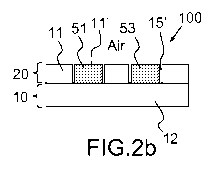
With regard to figures 2a to 2j, a switchable radiation source 100
that is directional in an IR band comprised in the 1 pm to 20 pm band and
according to the invention will be described.
In its structure, this source 100 comprises at least:
a substrate 10 providing a function of ensuring a temperature near
the critical temperature of the MIT, and a function as a primary source
of radiation, in said IR band, centered on the Wien wavelength of the
material from which it is made, the width of the band being given by
Planck's law; and
an external layer 20 intended to direct the radiation.
The external layer 20 comprises controllable cells 51 made of a
metal insulator transition (MIT) material; the phase transition occurs when
the
temperature passes the critical temperature Tc, the wavelength Ac (referred
to as the transition wavelength) corresponding to the critical temperature Tc
being located in the IR band of the source. The MIT possesses a crystalline
and therefore insulating phase referenced 11, and an amorphous phase,
which is electrically and thermally conductive because it is metallic,
referenced 11'. These cells 51 are associated with an electrical or thermal
CA 02892684 2015-05-26
8
means for controlling their temperature change and therefore their phase
change, shown in figures 4 and 6.
According to a first embodiment, the cells are formed in the
following way. Reference is made to figures 2a to 2j.
The substrate 10 is composed of a material 12 ensuring radiation
is emitted in an IR band centered on the Wien wavelength of the material. It
is for example a question of an MIT material such as V02, LaCr03 or a non-
MIT material such as SiC, Si or S131=14, the thickness of which is comparable
to or larger than the thermal wavelength, as shown in figures 2a and 2b. The
material chosen depends on the wavelength at which the source must
operate.
According to one alternative, the substrate may be made of the
same MIT material as that of the external layer, as shown in figures 2c to 2j,
but be intended to remain in its crystalline state 11. For this purpose, an
electrically and thermally insulating layer 15, of Si02 or silicon nitride for
example, typically from 10 nm to 50 nm in thickness, is deposited on the
substrate 11 by chemical deposition (CVD, PECVD, etc.) before the external
MIT layer 20 is deposited and over the entire surface of the substrate, then
etched as shown in figure 2c in order to prevent, in operation, the higher
temperature associated with the amorphous state 11' of the cells shown in
figure 2b from being transmitted to the substrate 11.
An MIT layer of about 2 pm in thickness is deposited on the
substrate 10 or on the insulating layer by cathode sputtering or PLD. This
MIT is typically:
LaCr03 with a Tc = 530 K corresponding to a Ac 5.5 pm; or
- BaTiO3 with a Tc = 393 K corresponding to a Ac 7.4 pm; or
- V02 with a Tc = 340 K corresponding to a Ac 8.5 pm; or
- V203 with a Tc =160 K corresponding to a Ac 18 pm.
The MIT material chosen is preferably a material the transition
wavelength Ac of which is closest to the Wien wavelength of the substrate 10.
More specifically Tc (and therefore Ac) is an average transition temperature
(wavelength, respectively) because the transition exhibits a hysteresis cycle
as illustrated in figure 3a for a 75 nm-thick sample of V02 deposited on a C-
CA 02892684 2015-05-26
9
plane sapphire substrate, in this case of A1203; Tc is the average of TCdown
and Tcup.
This MIT film is patterned with grooves, for example by optical
lithography, e-beam lithography, reactive ion etching or nanoimprint
lithography, so as to form furrows as shown in figures 2a to 2j. Thus, cells
51,
53 taking the form of furrows that are electrically and thermally insulated
from
each other by air 15' are obtained as may be seen in figures 2a, 2b, 2i and
2j.
Typically furrows that are about 2 pm wide and about 200 nm deep are
produced. This width advantageously enables emission in the range
considered, one cell in two being switched, or enables collective switching of
n adjacent cells in m, n and m being low numbers < 10. The grooves may of
course be formed in another direction in order then to obtain circular cells,
cells forming a chequerboard pattern, inter alia.
According to another alternative, furrows are formed directly on
the substrate 11 as shown in figures 2e and 2h. These furrows are coated
with insulator 15 (on their walls and bottom) as shown in figure 2f, then the
MIT material 11 is deposited in these furrows as shown in figure 2g.
According to one variant, a layer of insulator 15 is deposited in the bottom
of
the furrows but not on the walls, then the MIT 11 is deposited in the furrows,
and grooves are formed in order to ensure an insulating air gap 15' between
the walls of the furrows and the MIT 11, as shown in figures 2i and 2j.
Among these cells, certain (or all) are associated with control
means for controlling their phase transition and then become controllable
cells 51, the remaining cells 53 being uncontrollable. When the source is in a
hybrid configuration forming a certain sequence of crystalline/amorphous
states, i.e. when certain of the cells are in their amorphous state, said
cells
form a diffraction grating 50, as shown in figures 2b, 2j, 4b and 4c, that
modifies the emission pattern of the field existing at the substrate/external
MIT layer interface.
This grating 50 is preferably periodic, one- or two-dimensional in
the plane (xy) of the layer, and for example circular or chequered; it will be
recalled that the period P of the grating is related to Wien wavelength by the
relationship P-Aw/(2n), n being the refractive index of the medium. However,
= CA 02892684 2015-05-26
these cells could form an aperiodic diffraction grating the emission
directions
of which would then not have two-fold, four-fold or six-fold orientational
symmetry (invariant in rotation by 2pi/2, 2pi/4 and 2pi/6). Quasi-crystalline
or
Penrose-type tilings are examples of such gratings. Blazed gratings would
5 also allow the azimuthal symmetry of the emission to be broken.
In the case of an MIT substrate, the latter supports, at its interface
with the external layer 20, a surface mode also referred to as a surface
polariton, and hence its far-field emission is weak. When the external layer
is in its hybrid crystalline/amorphous configuration and the cells form a
10
diffraction grating 50, the surface mode supported by the substrate 10 is then
diffracted by said grating 50 and the thermal emission becomes directional in
the near field but also in the far field. Figure 3b shows the thermal emission
at 8.5 pm for a thermal source according to the invention, with emission that
is:
15
omnidirectional and very weak in the purely crystalline phase
(curve a); and
directional and centered on about +50 and -50 in the hybrid
phase (curve b).
When there is an insulating layer 15 between the MIT substrate
20 and the
external layer, the thickness of said layer is chosen to be small
relative to the attenuation length of the surface mode (i.e. the mode that
exists at the substrate/insulator interface); the surface mode then penetrates
partway into the insulator and is diffracted by the grating 50 of the external
layer 20.
Preferably, the substrate 10 is made of material able to support a
surface mode at the interface with the external layer 20 or with the insulator
15, this being the case for MITs or S102. If this is not the case, the
substrate
supports an evanescent field that will also be diffracted by the grating, but
then the emission will be very weakly directional.
The grating may be obtained differently depending on whether all
the cells are controllable or not.
In the case where all the cells are controllable 51, the grating is
obtained by controlling certain cells to their amorphous state and
CA 02892684 2015-05-26
11
others to a crystalline state, depending on the required diffraction
grating.
According to one variant, certain cells 53 are not controllable and
remain in an insulating and therefore crystalline state 11 if it is a
question of cells of MIT material; the grating is obtained by controlling
certain other cells (these cells therefore belonging to the controllable
group 51) or even all of these controllable cells to their amorphous
state. The latter case is illustrated in:
o figures 4a and 4b for a one-dimensional periodic grating 50 in
the plane xy, these figure showing:
- (for 1=0) all the cells (both the controllable cells 51 and
uncontrollable cells 53) in their crystalline state 11 and thus not
forming a diffraction grating (figure 4a); and
- (for 1=10) the controllable cells 51 in their amorphous
state 11' and the uncontrollable cells 53 in their crystalline state
11, thereby together forming a diffraction grating (figure 4b);
and
o figure 4c for a two-dimensional periodic grating 50 in the plane
xy, this figure showing (for I=10) the controllable cells 51 in their
amorphous state and the uncontrollable cells 53 in their
crystalline state, the controllable and uncontrollable cells
together forming a diffraction grating.
As has been seen, the means for controlling the MIT cells 51 may
be electrical. These means comprise electrodes 52 connected to a generator
of an electrical current that is optionally pulsed, for example about every
one
hundred ns to one ps, in order to make the MIT cells rapidly switchable. The
cells 51 require only a low electrical power, for example lower than a few
tens
of mW/cm2, thereby making it possible to achieve useful power/total power
ratios of much lower than 10% for the source.
The cells 51 may be controlled groupwise, the number of cells per
group possibly optionally varying from one group to another; the cells may
even be controlled individually, this corresponding to the case of a single
cell
per group. In figures 4a to 4c, the cells 51, which take the form of furrows
(1D
grating in the plane xy) or form a chequerboard pattern (2D grating in the
plane xy), are controlled individually.
CA 02892684 2015-05-26
,
12
The emission direction of the source depends on the period and
dimensions of the diffraction grating 50, as shown by the formula:
Km=(2Tc/X) sin 0 +m 27c/P
where Km is the parallel component of the diffracted wave of order m, 0 the
angle of emission and P the period of the grating.
It is possible to control the cells so as to choose the period of the
grating, this period being a multiple of the period of the cells.
By changing the period P of the grating, the emission direction of
to the source is then modulated as may be seen from the emissivity curves
(curves a, b and c) corresponding to the gratings in figures 5a, 5b and 5c,
respectively, and as shown in figure 5d for one wavelength. The period
and/or dimensions of the grating are therefore set depending on the desired
direction.
For this purpose, the means for controlling the cells 51 are
advantageously supervised by supervising means, in order to allow, on
request or automatically, these cells 51 to be actively modified depending on
the spatial characteristics desired for the diffraction grating 50 formed by
the
cells, and especially its desired periods (or optionally period if it has only
one)
and/or its desired dimensions, as illustrated in figure 5a for example. If P
is
the period in the direction Ox of the grating in figure 5a, there being two
cells
per period, one cell of which (in two) is intended to be amorphous, the
gratings in figures 5b and Sc have a new period P
. grating = 2P with 4 cells per
period, two cells of which (in 4) are intended to be amorphous in the grating
in figure 5b, and one cell of which (in 4) is intended to be amorphous in the
grating in figure 5c. For example, Pgrating = 4.565 pm for P = 2.282 pm.
To avoid the need for the electrical switching device and the need
to address the cells that this embodiment implies, another embodiment of the
invention, described with regard to figure 6, allows the grating to be formed
more spontaneously on the device scale. In this other embodiment, the
external layer 20 comprises:
-
a uniform external layer 22 made of said metal insulator transition
material, said layer being uniform in that it is not patterned with
grooves or etched; and
CA 02892684 2015-05-26
13
a subjacent layer 21 having a thermal conductivity that is spatially
modulated depending on the pattern of the cells to be obtained in the
external underlayer 22. It is typically a question of a layer of Si the
surface of which has been thermally oxidized through a mask, and
therefore with spatial selectivity, so as to allow zones of Si02 of much
lower thermal conductivity to be defined; it will be recalled that the
thermal conductivity of silicon is about 130 WrK/m whereas that of
silica is about 1.4 W/K/m, i.e. about a factor of 100 lower. The thermal
conductivity of this underlayer 21 is controlled by electrical means.
Preferably, as indicated above, this thermally conductive underlayer
consists of a material supporting a surface mode at its interface with
the external underlayer.
The substrate 13 is typically a thermally conductive Si substrate, in
order to allow excess heat to be removed from the thermal layer by
conduction.
The cells are then formed thermally via this high-thermal-
conductivity layer. Specifically, since this thermally conductive underlayer
comprises spatial zones 21a intended to become hotter than others 21b
under the action of a horizontal flux of electrical current that is initially
uniform, the transition takes place first for the least cooled and best
insulated
zones, thereby increasing their electrical conductivity, so that lines of flux
form in the external layer 22, above the well thermally insulated hot zones
21a, and thus cells analogous to those of the preceding embodiment are
produced. This thermally conductive underlayer 21 also controls the cells; in
this case it is a question of device-scale control.
Whatever its embodiment, this source is not a wire source but
rather a planar or almost planar source, i.e. a source with a radius of
curvature that is large relative to its thickness. Its area is determined
depending on the period of the grating; it must typically comprise at least
ten
periods. Thus, for an IR source centered on 10 pm and for a 1D grating of
4.5 pm period, its area is larger than 0.5 x 0.5 mm2.
As regards fields of application of this type of source, mention may
be made of:
CA 02892684 2015-05-26
14
domestic heating systems, or more generally systems for
managing heat flows;
- thermal control of industrial processes (chemistry, adhesive
bonding, etc.);
the food-processing field (ovens, drying, freeze-drying etc.);
the IR spectroscopy used to analyze gases; and
- stealthy IR sources.