Note: Descriptions are shown in the official language in which they were submitted.
CA 02896468 2015-06-25
WO 2014/011126
PCT/TR2012/000179
MULTIPOINT TOUCH SENSOR WITH ACTIVE MATRIX
The technical field of the invention
The invention is related to sensors (feedback mechanisms) of robotics and
devices.
Known status of the technique
It is well known that automation mimics the human body. It is observed that
the computation
systems for the data acquisition from sensors are basically a simple copy of
human brain as
well as the sensors are the simple copies of the receptors of the human body.
It is clear that
the automation systems with less than a hundred years of past, have a long way
in order to
reach the capability of human body with the experience of hundreds thousands
years of
evolution.
"Tactile Sensing", which is the topic of the invention, - with current
technology - is frequently
limited to sense an approaching metal or a material that the sensor is
sensitive and inform that
to main processor by using proximity sensors. As the data which is transmitted
by these
sensors include only "true" or "false" and they are lack of leveled
information, and they are
also bulky (few millimeters diameter), these sensors are not efficient for
multiple point
!0 applications.
Even for most developed humanoids, the technique that is currently being used
is very
expensive force/torque sensors, that are located on the joints. These sensors
measure the
contact pressure when an obstacle is in the way of the limb or when an object
has been
grasped. There exist one or more sensors and data acquisition systems for each
limb (arm-
15 elbow joint, fingers, etc.) in this detection/sensation method which
costs too much.
For the application when pressure sensors are used the geometrical dimension
becomes the
issue, again. Even if the geometrical problem is relatively solved than again
the transmission
of the data to the main processor becomes an issue. Expensive data acquisition
cards or
microcontrollers are being used for current applications, but when the input
numbers reach the
1
CA 02896468 2015-06-25
WO 2014/011126
PCT/TR2012/000179
level of hundred numbers; these inputs become a constraint/limiting factor.
Human body that
has been trying to be mimicked includes hundreds of thousands even millions of
receptors in
the fingertip, as it is known. And human brain processes all the data that are
coming from
these receptors very fast.
The most recent and similar robotic tactile sensing patent that is related to
the invention is
Koyoma and et. als.'s with number US20110067504A1, which is submitted at
05.29.2008 and
published at 03.24.2011. Optocouplers are suggested for tactile sensing, but
because of the
dimensions of these optocouplers for each fingertip of the humanoid, a single
sensor is
proposed. It is suggested that by placing one sensor for 5 millimeters with a
matrix format
will increase the quantity which means 9 sensors for 1 centimeter.
All related and similar patents have the common issues like, low sensitivity,
low quantity
sensor per one centimeter square (limited to number tens) and the constraints
on the data input
numbers.
Technical problems to be solved by the invention
With the invention, it is intended to increase the number of the quantity of
the sensors per one
centimeter square up to more than one million. It is also aimed to measure all
of these
millions of points' per one centimeter displacements each and proses the data
fast by avoiding
high costs.
Explanations of Figures
Figure 1: Optocoupler systems' elements
Figure 2: Symbolical view of the fiber optic cables assembly that is meant to
minimize the
used area of optocoupler systems' elements
Figure 3: Symbolical view of image sensors like CCD, CMOS etc.
Figure 4: Symbolical view of a CCD, CMOS etc. type of sensor being used like
the receiver
of the optocoupler (phototransistor).
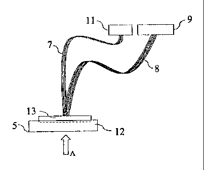
Figure 5: General view of the system elements.
2
CA 02896468 2015-06-25
WO 2014/011126
PCT/TR2012/000179
Figure 6: Array sequence of the fiber optic cables in the sensing area.
(Figure 5 ¨ "A"
direction view)
Figure 7: The displacement that is occurred proportional to the applied force
and the
corresponding image.
Figure 8: Virtually establishing different areas of the sensor to different
measuring areas
through fiber optic cables.
Figure 9: Optical system that is placed between fiber optics and the receiver
in the purpose to
coverage the beam of light because of the possible size mismatch.
Definitions of reference numbers on figures:
Every part in the figures are numbered and explained below.
1) Infrared (or normal) light source
2) Infrared (or normal) light receiver.
3) Reflecting light from the obstacle
4) The distance between the light source/receiver and the obstacle.
5) Light reflecting obstacle and the meantime the separator of the system from
the
surrounding environment.
6) Surrounding environment.
7) Fiber optic cables that carry the light from the source that is placed far
from the
measuring area.
8) Fiber optic cable that carries the light to the receiver that is placed far
from the
measuring area.
9) Webcam or a similar digital camcorder or digital camera sensor (CMOS, CCD
etc.)
10) Light capturing pixels meant to analyze connected light where each works
individually.
11) Light Source (Sum of more than one light source.)
12) Elastic Material
13) Rigid area; where fiber optic cables' tips are located and united with the
elastic area,
and which prevents the unwanted level of penetration.
14) Shape deformation when an object is penetrated through the elastic area.
3
CA 02896468 2015-06-25
WO 2014/011126
PCT/TR2012/000179
15)Bunch of cables consist of number 7 and 8 fiber optic cables.
16)The image that is composed by the sensors corresponding to the area where
there is no
deformation.
17) The image that is composed by the sensors corresponding to the area where
there is
deformation.
18) The connection areas that form groups, depending on the different
measurement areas
through the fiber optic cables that carry the light.
19) Optical system that makes the light beams closer. (Each material that is
used in the
system is infrared conductive)
20)Intensive bunch of beams of light (closer to each other).
Explanation of invention:
Optocouplers are one of the components that are frequently used in circuits of
encoders and in
other types of electronically circuits to provide electrical isolation.
Optocouplers include a
normal or infrared light source (1) and a light receptor (2) (Figure 1). There
are different types
of optocouplers. Such as; 1/0 which means true or false output type and
another type that
gives output proportional to the reflecting light intensity. This second type
of optocouplers
will be used for the invention. The beam/ray of light (3) that is delivered by
the light source
(1) will reflect from the obstacle (5) and will reach to the receptor (2).
Depending on the
distance between the obstacle and the receptor (4), voltage will be produced,
respectively.
Thus, measuring the distance(4) would be possible, depending on the
measurement of the
variation of voltage. Because of each light source's and sensor's diameter
which are a few
millimeters, usage of multiple optocouplers require a lot of space in
conventional designs.
The first aim of the invention is to enable to place a lot of receptors in a
small area by moving
away the optocouplers. Fiber optic cables (7) which are infrared conductive
and have
diameter less than 10 micrometers will carry and deliver the light from the
light source (1),
meanwhile equivalent fiber optic cables (8) with the same features will carry
the reflecting
light (3) to the receptor (2) (Figure 2). Because of the features of the fiber
optic cables such as
no noise or perturbation effect even if used parallel to each other and being
efficiently light
conductive even if the cables are bended or twisted, they can easily be used
in moving/mobile
fields. With current technology, standard infrared conductive fiber optic
cables have 9
micrometer diameters. It is calculated that (with the effect of loss areas
between the circles)
1.572.327 fiber optic cables can be placed in 1 centimeter square. Each light
sensor/receptor
requires one light source. With the sequence design in figure 6 each fiber
optic cable (8) that
4
CA 02896468 2015-06-25
WO 2014/011126
PCT/TR2012/000179
carries light to a sensor will own 3 fiber optic cables (7) that deliver light
from source. By that
the number of light delivering fiber optic cables (7) will one fourth of the
number of the
others (8). If the area loss of circles being next to each other and the loss
of light delivering
fiber optic cables (7) are taken into account there will be approximately
1.000.000 receptors
per 1 centimeter square. In other words there will be 1.000.000 points/pixels
that measure the
displacement.
Not every receptor (1) requires a corresponding light source (11); however
each measurement
point requires a corresponding receptor (2). Despite the fact that fiber optic
cables (7) (8)
solve the dimensional issues at the reception area, it results in an issue of
an overall system
dimension's being huge. But the real problem is acquiring and processing of
millions of data
rather than the dimensional issue. A voltmeter with one channel can only read
one, a two
channeled oscilloscope can read two, and a 32 analogues input data acquisition
card can read
32 data. Thus, any of these options are neither cost efficient nor close to a
convenient answer
to the requirement of reading all the data. With this invention, CMOS or CCD
sensor which
can be found in a conventional webcam or a similar camcorder or a digital
camera is utilized
to overcome above mentioned problem. Main advantage of these kinds of sensors
(9) is the
feature of containing millions of sensory pixels (10) depending on the
resolution of the
product. (Figure 3). Each sensory pixel (10) is able to detect 16.4 million
colors in standard
usage; therefore it is possible to measure the displacement precisely by the
variation of light.
In figure 4, the logic of light source (1) and the sensor (9) connection is
explained, briefly.
These image sensors (9) can be easily obtained by disassembling conventional
webcams. An
image sensor disassembled from any high definition webcam (HD ¨ 1920*1080
resolution =
2.073.600 pixels) can be connected to any computer via a universal serial bus
(USB) and is
able to convert over two million impulses to digital data. By pairing each
pixel (10) of the
sensor (9) with a corresponding fiber optic cable (8) it is assured to
transfer all light beams to
the processor on a single photo frame where the coordinates and the level of
displacements
are detected precisely by the aid of image processing techniques. With the
explanations till
now, it is assured that millions of receptors are placed in a small reception
area with precise
acquisition of data at a low cost. It is also mentioned that these acquired
data can be delivered
to the main processing unit in one cycle. But still this is not sufficient
enough for tactile
sensing. At this point the system can only detect diverging and converging
objects with high
resolution and sensitivity but the system cannot perceive the force and the
resultant tactile
feeling. More, when the touching take place the light source's (7) and the
receptor's (8) view
5
CA 02896468 2015-06-25
WO 2014/011126
PCT/TR2012/000179
will be blocked and nothing can be detected. In order to solve this issue
elastic modulus
(Young's Modulus) phenomenon is used. Elasticity can be imagined like a spring
characteristic coefficient of the objects that are not springs. An applied
force to an object will
cause a stretching (shape deformation). This deformation will be proportional
to the applied
force if the structure of the object is not damaged irreversibly. Thus, vice
versa the applied
force at the point of implementation can be calculated by the amount of the
shape deformation
on that point (if the elasticity coefficient of the object is known). In the
system, in order to
mimic the human tactile sensing there is a rigid area; where fiber optic
cables' tips are located
and unite with the elastic area, and also prevent the unwanted level of
penetration. The elastic
material (12) with the same elasticity of a human flesh is covered with a
layer (5) which
simulates the human skin and separates the surrounding environment and
guaranties the
reflection of light (Figure 5). Thus, when a penetration is occurred as in
figure 7 the thickness
of the elastic material (12) will decrease at these points (14), therefore the
intensity of the
reflecting light will increase (17) at that area. Each corresponding sensory
pixel (10) at that
area will detect the intensity of light and then with any image processing
technique the level
of penetration will be obtained. From the level of penetration and the
elasticity coefficient of
the material (12) the applied force will be calculated. Latter from the number
of triggered
pixels, the area of the deformation will be calculated and then by dividing
the applied force to
the area of deformation, the value of the pressure will be obtained. The
software will decide
the reaction of the robot or the device by comparing the pressure level with
the threshold
values that are already saved in the computer.
For instance if the penetration area is too small and the corresponding light
is close to white
(the intensity of light is too high) it will be understood that a needle type
of a sharp body has
sunk in. If so, the robot or the device will act like what it is programmed
to. This will be a
reflex program, meaning that the area of penetration can be drawn back.
Meanwhile if the robot or the device is needed for more heavy duties or does
not need to be as
sensitive as human skin, the elastic material (12) can be chosen with a less
elasticity feature.
Thus, the system will have a similar tactile sensing for bigger forces. After
a calibration for
the new material's elasticity module and light conductivity for the
calculations, the new
system will work.
It is known that the commercial thermal cameras are infrared cameras which
measure the
temperature. The color becomes brighter and whiter if the temperature
increases when
6
CA 02896468 2015-06-25
WO 2014/011126
PCT/TR2012/000179
recording with infrared cameras. The proposed system will also measure any
heat source near
the detection field. It will help to protect the device or robot form high
temperature because
the measurement will be close to white just like sharp body penetration
effect.
It is mentioned before that a sensor obtained from HD webcam contains more
than two
millions of pixels. A single component is able to contain more than twenty
millions of pixels
if a high definition digital camera is used, instead. One fingertip or any
other part of human
body can intensify that much of receptors. For this reason incoming fiber
optic cables (8)
from different sensory organs are located in virtual different areas (18) of
the image sensor
(9), therefore with one image sensor more than one sensory organ can be
measured.
Because of the variety of the used products and fiber optic cable (15)
diameters and pixel (10)
dimensions do not match with each other and a problem can arises. In order to
prevent this
issue beams/rays of light can be converged (20) to each other as in figure 9
through optical
system(s) (19). The used material for this optical system is also infrared
conductive.
The system can work with nearly every personal computer as well as industrial
computers by
connecting sensors like CMOS, CCD, etc. through an electronically circuit
specialized for this
system to the main processor of the device or robot.
Industrial application of the invention
This invention can answer to a lot of industrial fields that works with
automation systems
because the number of receptors per unit area is dramatically increased_and
the pressure and
force values can be obtained fast.
Some outstanding application areas; robotic sensing ¨ realizing the tactile
sensing of
humanoids; medical ¨ with more receptors a better feeling of touching to the
patient for
remote operations (haptic); increase the sensing abilities of landmine
scanning and bomb
disposal robots accordingly decreasing the chance of failure and adding the
temperature
measurement to tactile sensing in case needed.
7