Note: Descriptions are shown in the official language in which they were submitted.
CA 02897307 2015-07-14
1
WIDEBAND AND LOW-LOSS QUADRATURE PHASE QUAD-
FEEDING NETWORK FOR HIGH-PERFORMANCE GNSS ANTENNA
FIELD OF THE INVENTION
The present invention relates to antenna feed systems and, more particularly,
to
quadrature phase antenna feed systems.
BACKGROUND INFORMATION
Global navigation satellite system (GNSS) multi-band antennas are typically
utilized in
GNSS systems for improved performance. For GNSS multi-band antennas, multiple
feed
points may be utilized to increase the axial-ratio beamwidth and/or bandwidth
as well as
to improve the phase center variation (PCV) and phase center offset (PCO)
associated with the
antenna. Quadrature feed (quad feed) antennas, in which four feed points are
utilized are
common with GNSS antenna systems. However, a noted disadvantage of currently
available
quadrature feed systems is that they are single band and/or have a high loss.
Typically,
currently available quad direct feed systems only cover the Li band. This does
not provide
is adequate multi-band coverage that may be necessary for certain GNSS
operations.
SUMMARY OF THE INVENTION
The disadvantages of the prior art are overcome by providing a quadrature feed
antenna
system that has little loss and provides multi-band coverage. The quad feed
antenna system
20 comprises of a 1800 phase shifter followed by a pair of conventional 90
hybrid couplers. The
180 phase shifter utilizes a microstrip line phase reversal structure to
generate the 1800 phase
reversal. In an illustrative embodiment, the phase reversal structure
comprises a transition
from a microstrip to a parallel strip line before the phase reversal occurs.
After the phase
reversal occurs, the parallel strip line is then transitioned back to a
microstrip line. The phase
CA 02897307 2015-07-14
2
reversal structure provides a high bandwidth and low loss mechanism to enable
the phase
reversal to generate 00 and 1800 outputs that may be utilized by the hybrid
couplers to
generate the quadrature phase outputs for a GNSS system.
BRIEF DESCRIPTION OF THE DRAWINGS
The embodiments herein may be better understood by referring to the following
description in conjunction with the accompanying drawings in which like
reference numerals
indicate identically or functionally similar elements, of which:
Fig. 1 is a schematic block diagram of an exemplary quadrature fed antenna in
accordance with an illustrative embodiment of the present invention;
Fig. 2 is a schematic block diagram of an exemplary quadrature feeding network
system
in accordance with an illustrative embodiment of the present invention;
Fig. 3 is an exemplary diagram of a phase reversal structure in accordance
with an
illustrative embodiment of the present invention;
Fig. 4 is an exemplary diagram of a phase reversal structure showing cross
sectional
lines in accordance with an illustrative embodiment of the present invention;
Fig. 5 is a cross section of an exemplary phase reversal structure along a
microstrip line
section in accordance with an illustrative embodiment of the present
invention;
Fig. 6 is a cross section of an exemplary phase reversal structure along a
microstrip line
section in accordance with an illustrative embodiment of the present
invention;
Fig. 7 is a cross section of an exemplary phase reversal structure along a
microstrip line
section in accordance with an illustrative embodiment of the present
invention;
Fig. 8 is a cross section of an exemplary phase reversal structure along a
microstrip line
section in accordance with an illustrative embodiment of the present
invention;
Fig. 9 is a cross section of an exemplary phase reversal structure along a
microstrip line
section in accordance with an illustrative embodiment of the present
invention;
CA 02897307 2015-07-14
3
Fig. 10 is a cross section of an exemplary phase reversal structure along a
microstrip
line section in accordance with an illustrative embodiment of the present
invention;
Fig. 11 is a cross section of an exemplary phase reversal structure along a
microstrip
line section in accordance with an illustrative embodiment of the present
invention;
Fig. 12 is a cross section of an exemplary phase reversal structure along a
microstrip in
accordance with an illustrative embodiment of the present invention;
Fig. 13 is a circuit schematic of the exemplary phase reversal structure of
Fig. 3 in
accordance with an illustrative embodiment of the present invention;
Fig. 14 is a diagram illustrating an exemplary phase reversal structure in
accordance
with an illustrative embodiment of the present invention; and
Fig. 15 is a diagram illustrating an exemplary 180 degree phase shifter that
generates
two outputs having a 180 degree phase difference in accordance with an
illustrative
embodiment of the present invention.
DETAILED DESCRIPTION OF AN ILLUSTRATIVE EMBODIMENT
Fig. 1 is a schematic diagram of an exemplary quadrature fed antenna system
100 in
accordance with an illustrative embodiment of the present invention. The
antenna system 100
comprises of one or more antenna radiators 105 operatively interconnected with
a quad feed
network 110. The quadrature feed network 110 illustratively comprises of four
feed points
115 A-D that provide signals at various phases, including, for example 0 , 90
, 180 and
270 . Exemplary feed point 115A provides a 0 phase, feed point 115B provides
a 90 phase,
feed point 115C provides a 180 phase and feed point 115D provides a 270
phase. It should
be noted that the particular orientation of the feed points and the phases
entering the antenna
radiators are shown for illustrative purposes. As such the physical
orientation of feed points in
which phases are provided by particular feed points should be taken as
exemplary only.
Further, as will be appreciated by those skilled in the art, the actual values
of the outputs of
the quadrature feed system may differ in phase from that described were shown
herein. For
example, it is shown and described that the output has a 0, 90, 180 and 270
output; however,
in alternative embodiments, the outputs may differ. As such, the description
of specific
output phases should be taken as exemplary only.
CA 02897307 2015-07-14
4
It should be noted that in accordance with an illustrative embodiment of the
present
invention, the antenna radiator 105 may comprise any form of quad feed antenna
system. In
one illustrative embodiment, the antenna radiators may comprise a GNSS
antenna; however,
it is expressly contemplated that in alternative embodiments of the present
invention, differing
in types of antennas may be utilized. As such, the description of a GNSS
antenna being
utilized should be taken as exemplary only. Similarly, the quad feed network
110 is shown
for illustrative purposes of only. In a typical installation, a feed line (not
shown) would
provide for an input signal to the quad feed network 110.
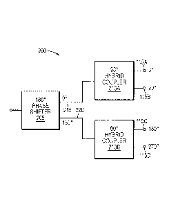
Fig. 2 is a schematic block diagram of an exemplary quadrature feed network
200 that
io may be utilized in accordance with an illustrative embodiment of the
present invention.
Illustratively, the quadrature feed network 200 comprises of a first and
second stage.
Illustratively, the first stage comprises of a 180 phase shifter 205 that
illustratively generates
two outputs 215, 220 that have a 180 phase difference, i.e., 0 and 180 . In
accordance with
an illustrative embodiment of the present invention, the 180 phase shifter
205 is implemented
using the teachings of the present invention. The second stage of the feed
network 200
illustratively comprises of a pair of 90 hybrid couplers 210A, B. Each of the
hybrid couplers
210 accepts an input signal and generates two output signals having a 90
phase difference.
Illustratively, the first hybrid coupler to 210A accepts an input phase of 0
and has output
phases of 0 at points 115A and 90 at point 115B. Similarly, the second
hybrid coupler 210B
accepts as an input signal 220 having a 180 phase and outputs at point 115 C
a 180 phase
signal and at point 115D a 270 phase signal.
Conventional 90 quadrature hybrid couplers 210 are readily available.
However,
180 phase shifters that have sufficiently wide bandwidth are difficult to
find commercially.
However, the present invention provides various embodiments of 180 phase
shifters that
may be utilized for an antenna feed network, such as a quad fed network.
Fig. 3 is an exemplary diagram of a phase reversal structure 300 in accordance
with an
illustrative embodiment of the present invention. Fig. 13 is a circuit diagram
illustrating the
circuit equivalent 1300 of the phase reversal structure of Fig. 3. The phase
reversal structure
300 illustratively comprises of a plurality of zones. Moving from left to
right in Fig. 3 are a
CA 02897307 2015-07-14
microstrip zone 305, a microstrip to parallel strip line transition zone 310,
a phase reversal
zone 315, a parallel strip line to microstrip transition zone 320 and a
microstrip zone 325. The
microstrip zones 305, 325 comprise conventional microstrips as are well-known
in the art.
The microstrip to parallel strip line zone 310 and the parallel strip line to
microstrip line zone
5 320 may be implemented using any technique for converting to/from
microstrip and parallel
strip lines. The phase reversal zone 315 illustratively comprises two vertical
plated via holes
that connects the strip lines to the ground metals located below. As a signal
traverses the
exemplary phase reversal structure 300 from left to right, the microstrip line
is transitioned to
a parallel strip line before the phase reversal structure 315 obtains the 180
phase reversal.
to The parallel strip line is then transitioned back to a microstrip and
the signal exits in zone 325
having a 180 phase difference.
Fig. 4 is an exemplary diagram of a phase reversal structure 300, such as that
shown in
Fig. 3, showing cross-sectional lines in accordance with an illustrative
embodiment of the
present invention. The phase reversal structure 300 illustrates a plurality of
cross sectional
is lines including, e.g., a microstrip cross-sectional line 500, a
microstrip cross-section 600, a
parallel strip line cross-section 700, two phase reversal cross-sections 800,
900, a second
parallel strip line cross section 1000, microstrip transition 1100 and a
microstrip cross-section
1200. Figs. 5-12, described further below, illustrate exemplary cross-sections
of the phase
reversal structured 300 at various points. These figures also illustrate
direction of the
20 electrical field flow showing a phase reversal between the input and
output. It should be noted
that t he exemplary cross-sections shown in Figs. 5-12, various elements may
not be to scale.
As such, the drawings can be taken as exemplary only and not scale
representations of the
widths, lengths and/or thicknesses of the various materials. As will be
appreciated by those
skilled in the art, the physical construction of microstrip and/or parallel
straight lines may
25 vary depending upon the desired frequency bandwidth, substrates, etc. As
these are design
choices that may vary depending upon the application for the quadrature fed
antennas system,
it should be noted that the figures are exemplary only.
CA 02897307 2015-07-14
6
Fig. 5 is a cross section of an exemplary phase reversal structure in
accordance with an
illustrative embodiment of the present invention. The cross-section shows a
portion of the
microstrip line 505 section of the phase reversal structure 300. The
microstrip line 505 is
located along a first surface of a substrate 520. A ground plane 510 is
located on the opposite
surface of the substrate 520. Electric fields 515 emanate from the microstrip
line 505 to the
ground plane 510. For purposes of the following figures, the direction of
travel of electrical
fields 515 is deemed to be in a 0 degree phase. That is, when a 180 phase
reversal is obtained,
the direction of the electrical fields will be reversed.
Fig. 6 is a cross section along line 600 of Fig. 4 of exemplary phase reversal
structure in
accordance with an illustrative embodiment of the present invention.
Illustratively, cross-
section 600 illustrates a portion of the microstrip line 505 wherein the top
conductor has
increased in size in preparation for the microstrip to parallel strip line
conversion, which
occurs along cross-sectional line 700 described further below in reference to
Fig. 7. The view
along cross-sectional line 600 is similar to the view along cross-sectional
line 500; however,
top conductor 505 has increased in size along line 600.
Fig. 7 is a cross section of an exemplary phase reversal structure at a
parallel strip line
cross-section 700 in accordance with an illustrative embodiment of the present
invention. Fig.
7 is a cross section of an exemplary phase reversal structure in accordance
with an illustrative
embodiment of the present invention. In Fig. 7, the cross section 700
illustrates a top
conductor 505 being substantially the same size as a bottom conductor 705. It
should be noted
that there is no longer a ground plane 510 along the bottom layer of the
substrate 520.
Instead, the ground plane 510 has narrowed to a second, parallel conductor
that is
substantially the same size as the top conductor 505. Electric fields 515
emanate from the top
conductor 505 to the bottom conductor 705 passing through the substrate 520.
Fig. 8 is a cross-section of an exemplary phase reversal structure at a first
phase reversal
zone cross-section 800 in accordance with an illustrative embodiment of the
present
invention. A cross-sectional view 800 illustrates the first of a series of
vias 810 that directly
CA 02897307 2015-07-14
7
transmit the incoming signal from the top conductor 505 to the bottom
conductor 705.
Illustratively, the plurality of vias 810 are arranged that pass through the
substrate 520. Other
portions of the top conductor 505 are etched out to leave sections 805. It
should be noted that
while two vias 810 are shown in exemplary cross-section 800, the principles of
the present
invention may work using any number of electrical electrically conductive
vias. As such, the
description of two vias as being utilized should to be taken as exemplary
only.
Fig. 9 is a cross-section of an exemplary phase reversal structure at a second
phase
reversal cross-section 900 in accordance with an illustrative embodiment of
the present
invention. At cross section 900, the sections 805 of top conductor from Fig. 8
are extended
through the substrate 520 to form a second set of vias 905 that interconnect
with the bottom
conductor 705. Vias 810, described above in relation to Fig. 8, continue as
conductors located
only on the top portion of substrate 520. It should be noted that at cross
section 900, the
electrical fields 915 have shifted phase 180 degrees and now emanate from the
bottom
conductor 705 and pass through the substrate 520 to top conductor 910.
Fig. 10 is a cross-section of an exemplary phase reversal structure
illustrating a parallel
strip line to microstrip line cross-section 1000 in accordance with an
illustrative embodiment
of the present invention. At cross section 1000, the top conductors 910 have
expanded to a
single top conductor 505. As will be appreciated by those skilled in the art,
cross section
1000 represents a 180 degree phase reversal of that shown in cross section
700.
Fig. 11 is a cross-section of an exemplary phase reversal structure
illustrating a cross-
section of 1100 in accordance with an illustrative embodiment of the present
invention. At
cross section 1100, the bottom conductor has expanded to become a ground plane
510. As
such, the parallel strip line has become a microstrip line with electrical
fields 915 flowing
from the ground place 510 to the top conductor 505. Fig. 12 is a cross-section
of an
illustrative exemplary phase reversal structure in a microstrip cross-section
1200 in
accordance with an illustrative embodiment of the present invention. Cross
section 1200 is
similar to cross section 1100, however, the top conductor 505 is smaller in
width.
The various cross sectional figures shown in Figs. 5-12 are shown to
illustrate an
= CA 02897307 2015-07-14
8
exemplary embodiment of a 180 degree phase reversal structure in accordance
with an
illustrative embodiment of the present invention. As will be appreciated by
those skilled in the
art, the exact sizes of conductors, vias, substrates as well as the materials
utilized may be
varied in accordance with design choices. As such, the description contained
above should be
taken to detail the general outline of a system that provides for the
generation of a 180 degree
phase difference output for use in a quadrature feed antenna network.
Fig. 14 is a diagram illustrating an exemplary phase reversal 1400 in
accordance with
an illustrative embodiment of the present invention. Phase reversal structure
1400 comprises
an alternative embodiment to the phase reversal structure 300 described above
in relation to
m Fig. 3. Exemplary phase reversal structure 1400 comprises of a microstrip
line 1410 that
comprises a plurality of vias 1420A,C to a ground place 1405. A second micro
strip line 1415
contains a via 1420B to the ground plane 1405. In exemplary phase reversal
structure 1400, a
signal entering the structure 1400 at a 0 degree phase on micro strip 1410,
leaves the phase
reversal structure 1400 at microstrip line 1415.
Fig. 15 is a diagram illustrating an exemplary 180 degree phase shifter
structure 1500 in
accordance with one embodiment of the present invention. Generally, the phase
shifter
structure 1500 comprises a phase reversal structure and generates two outputs
having a 180
degree phase difference. The phase shifter structure 1500 is illustratively an
alternative
embodiment the phase reversal structure described above in relation to Fig. 3.
Exemplary
phase shifter structure 1500 includes a microstrip line 1505 that enters a
power divider 1540
that sends a portion of the signal to a phase reversal module 300 and a
portion of the signal to
a bandpass filter module 1545. The phase reversal structure 300 is
illustratively shown with
two vias 1520A,B; however, it should be noted that in alternative embodiments,
varying
numbers of vias may be utilized. An output signal is provided at micro strip
1530 that is 180
degrees of the input signal 1505. The bandpass filter module 1545
illustratively comprises of
a shunted microstrip line filter. Exemplary bandpass filter module 1545
includes a microstrip
transmission line 1510 and a plurality of shunted short-circuited stubs
1515A,B. While two
shunted short circuit stubs are shown, it should be noted that in alternative
embodiments of
the present invention, differing numbers may be utilized. As such, the
description of two
CA 02897307 2015-07-14
9
shunted short circuit stubs should be taken to be exemplary only.
Illustratively, the shunted
short circuit stubs 1515 have an electrical length of approximately 90
degrees. Further, they
have a high characteristic impedance.