Language selection

Search

Patent 2898946 Summary

Third-party information liability

Some of the information on this Web page has been provided by external sources. The Government of Canada is not responsible for the accuracy, reliability or currency of the information supplied by external sources. Users wishing to rely upon this information should consult directly with the source of the information. Content provided by external sources is not subject to official languages, privacy and accessibility requirements.

Claims and Abstract availability

Any discrepancies in the text and image of the Claims and Abstract are due to differing posting times. Text of the Claims and Abstract are posted:

  • At the time the application is open to public inspection;
  • At the time of issue of the patent (grant).
(12) Patent: (11) CA 2898946
(54) English Title: MODULAR MULTI-STAGE INVERTER COMPRISING SURGE ARRESTER
(54) French Title: CONVERTISSEUR MODULAIRE MULTI-ETAGE POURVU D'UN CONDUCTEUR DE PROTECTION
Status: Granted and Issued
Bibliographic Data
(51) International Patent Classification (IPC):
  • H02M 07/49 (2007.01)
(72) Inventors :
  • DOMMASCHK, MIKE (Germany)
  • EBNER, GUNTER (Germany)
  • WURFLINGER, KLAUS (Germany)
(73) Owners :
  • SIEMENS ENERGY GLOBAL GMBH & CO. KG
(71) Applicants :
  • SIEMENS ENERGY GLOBAL GMBH & CO. KG (Germany)
(74) Agent: SMART & BIGGAR LP
(74) Associate agent:
(45) Issued: 2020-01-14
(86) PCT Filing Date: 2013-01-24
(87) Open to Public Inspection: 2014-07-31
Examination requested: 2017-11-24
Availability of licence: N/A
Dedicated to the Public: N/A
(25) Language of filing: English

Patent Cooperation Treaty (PCT): Yes
(86) PCT Filing Number: PCT/EP2013/051349
(87) International Publication Number: EP2013051349
(85) National Entry: 2015-07-22

(30) Application Priority Data: None

Abstracts

English Abstract


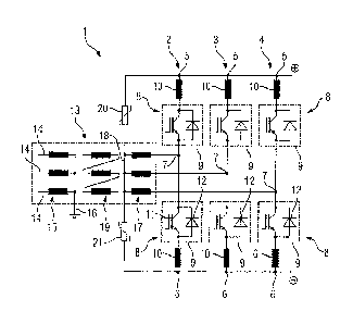
In order to provide an apparatus (1) for transmitting an electric power
between an AC
voltage grid and a DC voltage grid in the high-voltage range with phase
modules (2, 3,
4), which each have at least one common DC voltage connection (5, 6) and a
separate AC
voltage connection (7), wherein a phase module branch (8) extends between each
DC
voltage connection (5, 6) and each AC voltage connection (7) and has a series
circuit (9)
of two-pole submodules, which each have an energy store and a power
semiconductor
circuit which is connected in parallel with the energy store, with the result
that,
depending on the driving of the power semiconductor circuit at the two
submodule
connection terminals, either the voltage drop across the energy store or else
a zero
voltage can be generated, and an inverter transformer (13) which forms an
inverter
neutral point (18) on the secondary side and is connectable or connected on
the primary
side to an AC voltage grid (14) and on the secondary side to each AC voltage
connection
(7), in which apparatus improved protection against overloading is provided,
it is
proposed that at least one surge arrester (20, 21) is provided, which extends
between the
or one of the common DC voltage connections (5, 6) and the inverter neutral
point (7) of
the inverter transformer (13).


French Abstract

L'invention concerne un dispositif (1) qui permet de transmettre, dans le domaine des hautes tensions, une puissance électrique entre un réseau à tension alternative et un réseau à tension continue et qui comporte des modules de phase (2, 3, 4) dont chacun est pourvu d'au moins une connexion de tension continue (5, 6) commune ainsi que d'une connexion de tension alternative (7) séparée. Une branche de module de phase (8) s'étend entre chacune des connexions de tension continue (5, 6) et chacune des connexions de tension alternative (7) et comprend des sous-modules dipolaires qui sont montés en série (9) et comportent chacun un accumulateur d'énergie et un circuit à semi-conducteurs de puissance monté parallèlement à l'accumulateur d'énergie de telle manière que selon la commande du circuit à semi-conducteurs de puissance, la tension de chute de l'accumulateur d'énergie ou une tension nulle peut être générée aux deux bornes du sous-module. En outre, ledit dispositif comporte un transformateur de convertisseur (13) lequel constitue sur le côté secondaire un point neutre de convertisseur (18) qui est relié ou peut-être relié sur le côté primaire à un réseau à tension alternative (14) et sur le côté secondaire à chacune des connexions de tension alternative (7). Pour améliorer la protection contre les surcharges, le dispositif selon l'invention est pourvu d'au moins un conducteur de surtension (20, 21) s'étendant entre la ou les connexions de tension continue (5, 6) communes et le point neutre de convertisseur (7) du transformateur de convertisseur (13).

Claims

Note: Claims are shown in the official language in which they were submitted.


- 8 -
CLAIMS:
1. A device
for transferring electrical power between an
AC voltage network and a DC voltage network in a high-voltage
range, the device comprising:
a plurality of phase modules each having two shared
DC voltage terminals and each having a separate AC voltage
terminal;
a respective phase module branch extending between
each said DC voltage terminal and each said AC voltage
terminal, said phase module branch including a series circuit
with two-pole sub-modules each having two sub-module connection
terminals;
each said two-pole sub-module having an energy
storage device and a power semiconductor circuit connected in
parallel with said energy storage device, and wherein,
depending on a control of said power semiconductor circuit
either the voltage dropping across said energy storage device
or a zero voltage is generated at said two sub-module
connection terminals;
a converter transformer having a primary side
connected or connectable to an AC voltage network, said
converter transformer having a secondary side connected or
connectable to each said AC voltage terminal, and a converter
neutral point on said secondary side;
two surge arresters respectively connected between
one of said DC voltage terminals or a potential point having a
comparable potential and said converter neutral point; and

- 9 -
wherein the surge arresters are configured to protect
the submodules from overloading.
2. The device according to claim 1, wherein said sub-
modules at least partially form a half-bridge circuit.
3. The device according to claim 1, wherein said sub-
modules at least partially form a full-bridge circuit.
4. The device according to claim 1, wherein said
converter transformer has primary windings connected at a
grounded neutral point.

Description

Note: Descriptions are shown in the official language in which they were submitted.


CA 02898946 2015-07-22
PCT/EP2013/051349 - 1 -
2013P01510W0US
Description
MODULAR MULTI-STAGE INVERTER COMPRISING SURGE ARRESTER
The present invention relates to a device for transferring
electrical power between an AC voltage network and a DC voltage
network in the high-voltage range, including phase modules,
each having at least one shared DC voltage terminal and a
separate AC voltage terminal, wherein one phase module branch
extends between each DC voltage terminal and each AC voltage
terminal, which includes a series circuit made up of two-pole
submodules, each having an energy storage device and a power
semiconductor circuit connected in parallel with the energy
storage device, so that, depending on the control of the power
semiconductor circuit at the two submodule connection
terminals, either the voltage dropping across the energy
storage device or a zero voltage is able to be generated; and
including a converter transformer forming a neutral point on
the secondary side, which is connectable or is connected to an
AC voltage network on the primary side and to each AC voltage
terminal on the secondary side. The neutral point of the
secondary winding connected to the converter is referred to
below as the converter neutral point.
Such a device is already known from the established practice
under the term "modular multi-stage converter." Modular multi-
stage converters are, for example, used in the field of high-
voltage DC current transmission. Because of its modular
topology, the converter is easily scalable and may be easily
adapted to the particular requirements. The voltage at the AC
voltage terminals of the modular multi-stage converter may be
increased in stages, in which the level of the stages
corresponds to the voltage dropping across each energy storage
device. The power semiconductor circuit has power semiconductor
switches which are able to be switched on and off, in which so-

CA 02898946 2015-07-22
PCT/EP2013/051349 - la -
,
2013P01510W0US
called IGBTs in particular are used. Commercially available
IGBTs currently have a

CA 02898946 2015-07-22
PCT/EP2013/051349 - 2 -
A
2013201510W0US
blocking capacity of between 1.7 kV and 6.5 kV; thus, hundreds
of submodules are connected in series in the high-voltage
range. It is therefore possible to generate a virtually
harmonic voltage profile at the AC voltage terminal without a
requiring a great deal of filtering. To protect the power
semiconductor switches of the submodules, bypass switches are
provided which are situated between the submodule connection
terminals and via which a bridging of each associated module is
made possible. In the event of overloading of the entire
converter, the danger exists that all bypass switches will be
inadvertently fired. However, this may result in disadvantages.
The object of the present invention is therefore to provide a
device of the kind initially specified, in which improved
protection from overloading is provided.
The present invention achieves this object in that at least one
surge arrester is provided which extends between the or one of
the shared DC voltage terminals and the converter neutral point
of the converter transformer.
According to the present invention, it is provided to arrange
surge arresters between the DC voltage terminals and the
converter-side transformer neutral point. Within the scope of
the present invention, the surge arrester does not necessarily
have to be directly connected to the DC voltage terminal. It
may also extend between the converter neutral point and a
potential point which lies between the power electronics
component of each phase module branch and an inductor, for
example, a DC voltage choke. Within the scope of the present
invention, it is essential that the potential dropping across
the surge arrester is comparable to the potential between the
converter neutral point and the DC voltage terminal in question
and that it is co-determined by this potential. This enables
the use of surge arresters for protecting an initially
specified modular multi-stage converter. Surge arresters

CA 02898946 2015-07-22
PCT/EP2013/051349 - 2a -
2013P01510W0US
generally have a characteristic curve from which a ratio
between

=
CA 02898946 2015-07-22
PCT/EP2013/051349 - 3 -
2013P01510WOUS
the avalanche voltage and the operating voltage of
approximately 1.6 to 2.0 results. If such a surge arrester were
to be connected in parallel with a phase module branch, i.e.,
arranged between the DC voltage terminal and the AC voltage
terminal, it would be able to provide no protection. In the
currently known submodules, the triggering voltage of the
bypass switch of each submodule is approximately 1.5 per-units
of the maximum operating voltage. Effective protection would
therefore not be possible with a surge arrester. The present
invention is based on the discovery that the voltage dropping
across a phase module branch is of the order of magnitude of
the DC voltage which drops across the entire device on the DC
voltage side. In contrast, the difference in potential between
the shared DC voltage terminal and the converter neutral point
is only approximately half of the DC voltage which drops across
the entire device on the DC voltage side. Therefore, if the
surge arrester is connected between the converter neutral point
of the converter transformer and the shared DC voltage
terminal, effective protection of the phase module branches is
achieved by the present invention. Within the scope of the
present invention, it is under no circumstances required for
the voltage to be split symmetrically between the DC voltage
terminals with respect to the ground potential, i.e., for
example, at +300 kV and -300 kV. Within the scope of the
present invention, one of the DC voltage terminals may, for
example, be at a potential near the ground potential or a
medium-voltage potential, while the other DC voltage terminal
is, for example, at +600 kV.
Within the scope of the present invention, the power
semiconductor circuit has power semiconductor switches which
are able to be switched on as well as switched off. Such power
semiconductor switches are, for example, IGBTs, GT0s, IGCTs or
the like. A flyback diode is inversely connected in parallel
with each of these power semiconductor switches which are able
be

CA 02898946 2015-07-22
PCT/EP2013/051349 - 3a -
2013P01510WOUS
switched on and off. However, alternatively, reverse-conducting
power semiconductor switches may also be used.

CA 02898946 2015-07-22
PCT/EP2013/051349 - 4 -
-
2013P01510W0US
Within the scope of the present invention, the design of the
power semiconductor circuit is generally arbitrary.
However, the submodules advantageously at least partially form
a half-bridge circuit. In a half-bridge circuit, the power
semiconductor circuit is made up of a series circuit made up of
two power semiconductor switches which are able to be switched
on and off, in which the series circuit is connected in
parallel with the energy storage device. A first submodule
connection terminal is connected to the potential point between
the power semiconductor switches of the series circuit. The
second submodule connection terminal is connected directly to
one pole of the energy storage device.
Alternatively or additionally, it is possible to form the
submodules completely or at least partially as a full-bridge
circuit. In a full-bridge circuit, two series circuits are
provided, each made up of two power semiconductor switches
which are able to be switched on and off, in which both series
circuits are connected in parallel with the energy storage
device. A first submodule connection terminal is connected to
the potential point between the power semiconductor switches,
which are able to be switched on and off, of the first series
circuit, and the second submodule connection terminal is
connected to the potential point between the power
semiconductor switches, which are able to be switched on and
off, of the second series circuit.
Advantageously, each phase module branch has DC voltage
terminals, wherein two surge arresters are provided, each
extending between one of the DC voltage terminals and the
converter neutral point. Within the scope of the present
invention, the device has phase modules, the number of which
corresponding to the number of phases of the connected AC
voltage network. Each phase of the AC voltage network is
connected to one of the AC voltage terminals via the converter

CA 02898946 2015-07-22
PCT/EP2013/051349 - 4a -
,
2013P01510WOUS
transformer. In addition, two unequally polarized DC voltage
terminals are provided which are at a positive

81788365
- 5 -
DC voltage potential or a negative DC voltage potential with
respect to the ground potential. For example, the voltage drop
between the positive DC voltage terminal and the negative DC
voltage terminal of the device is 600 kV. This total voltage,
which is symmetrically distributed to the two DC voltage lines,
is +300 kV or -300 kV with respect to the ground potential.
Alternatively, one of the DC voltage terminals is at ground
potential.
Advantageously, the converter transformer has primary windings
which form a grounded neutral point, in which compensating
windings are provided which are connected to each other in a
delta configuration.
According to another aspect of the present invention, there is
provided a device for transferring electrical power between an
AC voltage network and a DC voltage network in a high-voltage
range, the device comprising: a plurality of phase modules each
having two shared DC voltage terminals and each having a
separate AC voltage terminal; a respective phase module branch
extending between each said DC voltage terminal and each said
AC voltage terminal, said phase module branch including a
-series circuit with two-pole sub-modules each having two sub-
module connection terminals; each said two-pole sub-module
having an energy storage device and a power semiconductor
circuit connected in parallel with said energy storage device,
and wherein, depending on a control of said power semiconductor
circuit either the voltage dropping across said energy storage
device or a zero voltage is generated at said two sub-module
connection terminals; a converter transformer having a primary
side connected or connectable to an AC voltage network, said
converter transformer having a secondary side connected or
CA 2898946 2019-01-15

. .
81788365
- 5a -
connectable to each said AC voltage terminal, and a converter
neutral point on said secondary side; two surge arresters
_
respectively connected between one of said DC voltage terminals
or a potential point having a comparable potential and said
converter neutral point; and wherein the surge arresters are
configured to protect the submodules from overloading.
Additional advantageous embodiments and advantages of the
present invention are the subject matter of the following
description of exemplary embodiments of the present invention
with reference to the figure of the drawing, in which the
figure schematically illustrates one exemplary embodiment of
the device according to the present invention.
Figure 1 shows one exemplary embodiment of the device 1
according to the present invention. The device 1 has three
-phase modules 2, 3, and 4, each having a positive shared DC
voltage terminal 5 and a negative shared DC voltage terminal 6.
In addition, each of the phase modules 2, 3, and 4 is equipped
with an AC voltage terminal 7. Phase module branches 8 extend
between each of the shared DC voltage terminals 5 or 6 and each
AC voltage terminal 7, each having a series circuit made up of
two-pole submodules 9 and an inductor 10, which are connected
to each other in series. The sequence of the submodules 9 and
the inductor 10 is arbitrary. Each phase module 2, 3, and 4
therefore has two phase module branches 8 arranged in series.
The series circuit made up of two-pole submodules 9 is only
schematically depicted, in which it is indicated that the
=
CA 2898946 2019-01-15

a
CA 02898946 2015-07-22
PCT/EP2013/051349 - 6 -
2013P01510W0US
series circuit has IGBTs 11 as power semiconductor switches
which are able to be switched on and off, in which a flyback
diode 12 is inversely connected in parallel to each IGBT 11.
However, expressed more precisely, the two-pole submodules 9 in
the exemplary embodiment depicted in the figure form a so-
called half-bridge circuit, in which each submodule has an
energy storage device and a series circuit which is connected
in parallel to this energy storage device which is made up of
two IGBTs 11, each having an inverse flyback diode 12. One of
the submodule connection terminals is connected to the
potential point between the two IGBTs 11. The other submodule
connection terminal is connected directly to one of the poles
of the energy storage device. Thus, depending on the control of
the IGBTs 11, it is possible to generate either the voltage
dropping across the energy storage device positively or
negatively, or a zero voltage, between the submodule connection
terminals in question.
From the figure, it is furthermore apparent that the AC voltage
terminals 7 of the phase modules, 2, 3, 4 are connected to
phases 14 of an AC voltage network, which is otherwise not
further depicted, via a converter transformer 13. The converter
transformer 13 is equipped with primary windings 15 which are
connected to each other at a grounded neutral point 16. The
secondary windings 17 of the converter transformer 13 are
connected to each other at a secondary-side converter neutral
point 18 which, however, is not grounded. Compensating windings
19 are apparent between the primary windings 15 and the
secondary windings 17, which are connected to each other in a
delta configuration.
To protect the phase modules 8 which are connected to each
other at a Graetz bridge, and thus the total device, from
surges, two surge arresters 20 and 21 are provided, each
extending between one of the shared DC voltage terminals 5 or 6
and the converter neutral point 18.

A #
CA 02898946 2015-07-22
PCT/EP2013/051349 - 7 -
,
2013P01510WOUS
The present invention is based on the discovery that the
maximum operating voltage between the AC voltage terminal 7
and, for example, the shared positive DC voltage terminal 5,
may be on the order of the voltage dropping between the shared
DC voltage terminals 5 and 6. Due to the response behavior of
the surge arrester, this circuit variant is able to provide no
effective protection via a surge arrester directly via the
phase module branch 8. The AC voltage-side connection of the
surge arresters 20 and 21 to the converter neutral point 18 has
the advantage that the operating voltage dropping across each
surge arrester 20, 21 is on the order of magnitude of half the
maximum DC voltage which drops between the DC voltage terminals
and 6. Thus, in the case of internal converter faults, the
surge arresters 20 and 21 are transferred from their high-
resistance state to the low-resistance state before the
protection device of the submodules of the phase modules 2, 3
and 4 engages.

Representative Drawing
A single figure which represents the drawing illustrating the invention.
Administrative Status

2024-08-01:As part of the Next Generation Patents (NGP) transition, the Canadian Patents Database (CPD) now contains a more detailed Event History, which replicates the Event Log of our new back-office solution.

Please note that "Inactive:" events refers to events no longer in use in our new back-office solution.

For a clearer understanding of the status of the application/patent presented on this page, the site Disclaimer , as well as the definitions for Patent , Event History , Maintenance Fee  and Payment History  should be consulted.

Event History

Description Date
Inactive: Recording certificate (Transfer) 2023-02-23
Inactive: Multiple transfers 2023-01-25
Common Representative Appointed 2020-11-07
Grant by Issuance 2020-01-14
Inactive: Cover page published 2020-01-13
Pre-grant 2019-11-15
Inactive: Final fee received 2019-11-15
Common Representative Appointed 2019-10-30
Notice of Allowance is Issued 2019-05-21
Letter Sent 2019-05-21
Notice of Allowance is Issued 2019-05-21
Inactive: Q2 passed 2019-05-10
Inactive: Approved for allowance (AFA) 2019-05-10
Amendment Received - Voluntary Amendment 2019-01-15
Inactive: S.30(2) Rules - Examiner requisition 2018-08-03
Inactive: Report - No QC 2018-07-31
Letter Sent 2017-12-01
Request for Examination Received 2017-11-24
Request for Examination Requirements Determined Compliant 2017-11-24
All Requirements for Examination Determined Compliant 2017-11-24
Inactive: Cover page published 2015-08-14
Inactive: First IPC assigned 2015-08-04
Inactive: Notice - National entry - No RFE 2015-08-04
Inactive: IPC assigned 2015-08-04
Application Received - PCT 2015-08-04
National Entry Requirements Determined Compliant 2015-07-22
Application Published (Open to Public Inspection) 2014-07-31

Abandonment History

There is no abandonment history.

Maintenance Fee

The last payment was received on 2019-12-03

Note : If the full payment has not been received on or before the date indicated, a further fee may be required which may be one of the following

  • the reinstatement fee;
  • the late payment fee; or
  • additional fee to reverse deemed expiry.

Patent fees are adjusted on the 1st of January every year. The amounts above are the current amounts if received by December 31 of the current year.
Please refer to the CIPO Patent Fees web page to see all current fee amounts.

Owners on Record

Note: Records showing the ownership history in alphabetical order.

Current Owners on Record
SIEMENS ENERGY GLOBAL GMBH & CO. KG
Past Owners on Record
GUNTER EBNER
KLAUS WURFLINGER
MIKE DOMMASCHK
Past Owners that do not appear in the "Owners on Record" listing will appear in other documentation within the application.
Documents

To view selected files, please enter reCAPTCHA code :


To view images, click a link in the Document Description column (Temporarily unavailable). To download the documents, select one or more checkboxes in the first column and then click the "Download Selected in PDF format (Zip Archive)" or the "Download Selected as Single PDF" button.

List of published and non-published patent-specific documents on the CPD .

If you have any difficulty accessing content, you can call the Client Service Centre at 1-866-997-1936 or send them an e-mail at CIPO Client Service Centre.

({010=All Documents, 020=As Filed, 030=As Open to Public Inspection, 040=At Issuance, 050=Examination, 060=Incoming Correspondence, 070=Miscellaneous, 080=Outgoing Correspondence, 090=Payment})


Document
Description 
Date
(yyyy-mm-dd) 
Number of pages   Size of Image (KB) 
Description 2015-07-21 11 343
Representative drawing 2015-07-21 1 13
Drawings 2015-07-21 1 18
Claims 2015-07-21 2 54
Abstract 2015-07-21 1 31
Description 2019-01-14 12 393
Claims 2019-01-14 2 47
Abstract 2019-05-20 1 31
Representative drawing 2020-01-01 1 11
Notice of National Entry 2015-08-03 1 192
Reminder - Request for Examination 2017-09-25 1 117
Acknowledgement of Request for Examination 2017-11-30 1 174
Commissioner's Notice - Application Found Allowable 2019-05-20 1 162
Examiner Requisition 2018-08-02 3 148
International search report 2015-07-21 2 66
Amendment - Abstract 2015-07-21 2 106
National entry request 2015-07-21 3 76
Request for examination 2017-11-23 2 83
Amendment / response to report 2019-01-14 8 263
Final fee 2019-11-14 2 68