Note: Descriptions are shown in the official language in which they were submitted.
CA 02900407 2015-08-05
WO 2014/149619
PCT/US2014/019900
INTEGRATED ELEVATED APERTURE LAYER AND DISPLAY APPARATUS
RELATED APPLICATIONS
[0001] The present Application for Patent claims priority to U.S. Utility
Application No.
13/842,436, entitled "Integrated Elevated Aperture Layer and Display
Apparatus," filed
March 15, 2013, and assigned to the assignee hereof and hereby expressly
incorporated by
reference herein.
TECHNICAL FIELD
[0002] This disclosure relates to the field of electromechanical systems
(EMS), and in
particular, to an integrated elevated aperture layer for use in a display
apparatus.
DESCRIPTION OF THE RELATED TECHNOLOGY
[0003] Certain displays are constructed by attaching a cover sheet having an
aperture layer
to a substrate that supports a plurality of display elements. The aperture
layer includes
apertures that correspond to respective display elements. In such displays,
the alignment of
the apertures and the display elements affects image quality. Accordingly,
when attaching
the cover sheet to the substrate, extra care is taken to make sure that the
apertures are closely
aligned with the respective display elements. This increases the cost of
assembling such
displays. Further, such displays also include spacers that are used to
maintain a reasonably
safe distance between the cover sheet and the nearby display elements
supported by the
substrate to reduce the risk of damage caused by external forces, such as a
person pressing on
the display. These spacers are also expensive to manufacture thereby
increasing the
manufacturing costs. In addition, a large distance between the cover sheet and
the display
elements adversely affects image quality. In particular, it reduces the
contrast ratio of a
display. To decrease the distance, the cover sheet and substrate can be
coupled together with
only a small gap between the two, however, this can increase the risk of
damage if the display
elements and cover sheet contact one another.
SUMMARY
[0004] The systems, methods and devices of the disclosure each have several
innovative
aspects, no single one of which is solely responsible for the desirable
attributes disclosed
herein.
1
CA 02900407 2015-08-05
WO 2014/149619
PCT/US2014/019900
[0005] An innovative aspect of the subject matter described in this disclosure
can be
implemented in an apparatus that includes an apparatus that includes a
transparent substrate, a
light blocking elevated aperture layer (EAL), a plurality of anchors for
supporting the EAL
over the substrate, and a plurality of display elements. The EAL defines a
plurality of apertures
formed therethrough. The plurality of display elements are positioned between
the substrate
and the EAL. Each of the display elements corresponds to at least one
respective aperture of
the plurality of apertures defined by the EAL and each display element
includes a movable
portion supported over the substrate by a corresponding anchor that supports
the EAL over the
substrate. In some implementations, the display elements include
microelectromechanical
systems (MEMS) shutter-based display elements.
[0006] In some implementations, the apparatus includes a second substrate
positioned on a
side of the EAL opposite to the substrate. In some such implementations, the
EAL can be
adhered to a surface of the second substrate. In some other of such
implementations, the
apparatus includes a layer of reflective material deposited on one of a
surface of the EAL
nearest the second substrate and the second substrate facing the EAL.
[0007] In some implementations, the EAL includes at least one of a plurality
of ribs and a
plurality of anti-stiction projections extending towards the substrate. In
some other
implementations, the apparatus includes light dispersion elements disposed in
optical paths
passing through the apertures defined by the EAL. In some such
implementations, the light
dispersion elements include at least one of a lens and a scattering element.
In some other of
such implementations, the light dispersion element includes a patterned
dielectric.
[0008] In some implementations, the apparatus includes a plurality of
electrically isolated
conductive regions corresponding to respective display elements. In some such
implementations, the electrically isolated conductive regions are electrically
coupled to
portions of the respective display elements.
[0009] In some implementations, the apparatus also includes a display, a
processor, and a
memory device. The processor can be configured to communicate with the display
and to
process image data. The memory device can be configured to communicate with
the
processor. In some implementations, the apparatus also includes a driver
circuit configured
to send at least one signal to the display. In some such implementations, the
processor is
further configured to send at least a portion of the image data to the driver
circuit. In some
other implementations, the apparatus also can include an image source module
configured to
2
CA 02900407 2015-08-05
WO 2014/149619
PCT/US2014/019900
send the image data to the processor. The image source module can include at
least one of a
receiver, a transceiver, and a transmitter. In some other implementations, the
apparatus
includes an input device configured to receive input data and to communicate
the input data
to the processor.
[0010] Another innovative aspect of the subject matter described in this
disclosure can be
implemented in a method of forming a display apparatus. The method includes
fabricating a
plurality of display elements on a display element mold formed on a substrate.
The display
elements include corresponding anchors for supporting portions of the
respective display
elements over the substrate. The method also includes depositing a first layer
of sacrificial
material over the fabricated display elements and patterning the first layer
of sacrificial
material to expose the display element anchors. The method also includes
depositing a layer
of structural material over the first layer of sacrificial material such that
the deposited
structural material is deposited in part on the exposed display anchors and
patterning the layer
of structural material to define a plurality of apertures therethrough
corresponding to
respective display elements to form an elevated aperture layer (EAL). In
addition, the
method includes removing the display element mold and the first layer of
sacrificial material.
[0011] In some implementations, the method also includes depositing a second
layer of
sacrificial material over the first layer of sacrificial material and
patterning the second layer
of sacrificial material to form a mold for a plurality of EAL stiffening ribs
or a plurality of
anti-stiction projections extending from the EAL towards the suspended
portions of the
respective display elements. In some other implementations, the method
includes bringing
regions of the EAL into contact with a surface of second substrate such that
the regions of the
EAL adhere to the surface of the second substrate. In some other
implementations, the
method includes depositing a layer of dielectric over the layer of structural
material and
patterning the layer of dielectric to define light dispersion elements over
the apertures defined
through the layer of structural material.
[0012] In some implementations, the layer of structural material includes a
conductive
material. In some of such implementations, patterning the layer of structural
material
electrically isolates neighboring regions of the EAL. Each electrically
isolated region of the
EAL can be electrically coupled to the suspended portion of a respective
display element.
[0013] Another innovative aspect of the subject matter described in this
disclosure can be
implemented in an apparatus that includes a substrate, an EAL that defines a
plurality of
3
CA 02900407 2015-08-05
WO 2014/149619
PCT/US2014/019900
apertures formed therethrough. The EAL also includes a polymer material
encapsulated by a
structural material. The apparatus also includes a plurality of display
elements positioned
between the substrate and the EAL. Each display element corresponds to a
respective
aperture of the plurality of apertures.
[0014] In some other implementations, the apparatus includes a light absorbing
layer
deposited on a surface of the EAL. In some other implementations, the
substrate includes a
layer of light-blocking material. In some such implementations, the layer of
light-blocking
material defines a plurality of substrate apertures corresponding to
respective apertures of the
EAL.
[0015] In some implementations, the structural material includes at least one
of a metal, a
semi-conductor, and a stack of materials. In some other implementations, the
EAL includes a
first structural layer, a first polymer layer and a second structural layer
such that the first
structural layer and the second structural layer encapsulate the first polymer
layer.
[0016] In some implementations, the EAL includes a plurality of electrically
isolated
conductive regions corresponding to respective display elements. In some such
implementations, the electrically isolated conductive regions are electrically
coupled to
portions of the respective display element. In some other of such
implementations, the
electrically isolated conductive regions are electrically coupled to the
portions of the
respective display elements via anchors that support the respective display
elements over the
substrate. In some such implementations, the anchors supporting the portions
of the
respective display elements over the substrate also support the EAL over the
display
elements.
[0017] Another innovative aspect of the subject matter described in this
disclosure can be
implemented in a method of forming a display apparatus. The method includes
forming a
plurality of display elements on a display element mold formed on a substrate,
depositing a
first layer of sacrificial material over the display elements, patterning the
first layer of
sacrificial material to expose a plurality of anchors, forming an elevated
aperture layer (EAL)
over the first layer of sacrificial material, and removing the display element
mold and the first
layer of sacrificial material.
[0018] Forming the EAL can include depositing a first layer of structural
material over the
first layer of sacrificial material such that the deposited structural
material is deposited in part
on the exposed anchors, patterning the first layer of structural material to
define a plurality of
4
CA 02900407 2015-08-05
WO 2014/149619
PCT/US2014/019900
lower EAL apertures corresponding to respective display elements, depositing a
layer of
polymer material over the first layer of structural material, patterning the
layer of polymer
material to define a plurality of middle EAL apertures substantially in
alignment with
corresponding lower EAL apertures, depositing a second layer of structural
material over the
layer of polymer material to encapsulate the layer of polymer material between
the first layer
of structural material and the second layer of structural material, and
patterning the second
layer of structural material to define a plurality of upper EAL apertures
substantially in
alignment with corresponding middle and lower EAL apertures.
[0019] In some implementations, the exposed anchors support portions of
corresponding
display elements over the substrate. In some other implementations, the
exposed anchors are
distinct from a set of anchors supporting portions of the display elements
over the substrate.
[0020] In some implementations, the method further includes depositing at
least one of a
light absorbing layer or a light reflective layer over the second layer of
structural material.
[0021] Another innovative aspect of the subject matter described in this
disclosure can be
implemented in an apparatus that includes a transparent substrate, a display
element formed
on the substrate, a light blocking EAL supported over the substrate by an
anchor formed on
the substrate, and an electrical interconnect disposed on the EAL for carrying
an electrical
signal to the display element. The EAL has an aperture formed through it that
corresponds to
the display element. In some implementations, the EMS display element include
microelectromechanical systems (MEMS) shutter-based display element.
[0022] In some implementations, the apparatus further includes at least one
electrical
component coupled to the electrical interconnect. In some such
implementations, the
electrical interconnect is coupled to a first electrical component of the at
least one electrical
component corresponding to the display element and to a second electrical
component of the
at least one electrical component corresponding to a second display element
formed on the
substrate. In some such implementations, the electrical component includes at
least one of
one of a capacitor and a transistor coupled to the electrical interconnect. In
some such
implementations, the transistor includes an indium gallium zinc oxide (IGZO)
channel.
[0023] In some implementations, the electrical interconnect is electrically
coupled to the
anchor such that the anchor transmits the electrical signal to the display
element. In some
other implementations, the electrical interconnect includes one of a data
voltage interconnect,
a scan-line interconnect or a global interconnect. In some implementations,
the apparatus
CA 02900407 2015-08-05
WO 2014/149619
PCT/US2014/019900
includes a dielectric layer separating the electrical interconnect from the
EAL. In some other
implementations, the apparatus includes a second electrical interconnect
disposed on the
substrate electrically coupled to a plurality of display elements.
[0024] In some implementations, the EAL includes an electrically isolated
conductive
region corresponding to the display element. In some such implementations, the
electrically
isolated conductive region is electrically coupled to a portion of the display
element. In some
implementations, the electrically isolated conductive region is electrically
coupled to the
portion of the display element via a second anchor that supports the display
element over the
substrate. In some other implementations, the anchor supporting the EAL over
the substrate
also supports a portion of the display element over the substrate, and the
electrically isolated
conductive region is electrically coupled to the suspended portion of the
display element via
the anchor.
[0025] In some implementations, the apparatus also includes a display, a
processor, and a
memory device. The processor can be configured to communicate with the display
and to
process image data. The memory device can be configured to communicate with
the
processor. In some implementations, the apparatus also includes a driver
circuit configured
to send at least one signal to the display. In some such implementations, the
processor is
further configured to send at least a portion of the image data to the driver
circuit. In some
other implementations, the apparatus also can include an image source module
configured to
send the image data to the processor. The image source module can include at
least one of a
receiver, a transceiver, and a transmitter. In some other implementations, the
apparatus
includes an input device configured to receive input data and to communicate
the input data
to the processor.
[0026] Another innovative aspect of the subject matter described in this
disclosure can be
implemented in a method of manufacturing a display apparatus. The method
includes
providing a transparent substrate and forming a display element on the
substrate. A light
blocking layer is formed over the substrate, supported by an anchor formed on
the substrate.
The method further includes forming an aperture through the light blocking
layer to form an
EAL, where the aperture corresponds to the display element. An electrical
interconnect is
formed on top of the EAL for carrying an electrical signal to the display
element.
[0027] In some implementations, the method includes depositing a layer of
electrically
insulating material over the EAL prior to forming the electrical interconnect.
In some such
6
CA 02900407 2015-08-05
WO 2014/149619
PCT/US2014/019900
implementations, the EAL includes a conductive material and the method further
includes
patterning the layer of electrically insulating material to expose portions of
the EAL prior to
forming the electrical interconnect. Forming the electrical interconnect can
include
depositing a layer of conductive material over the layer of electrically
insulating material and
patterning the layer of electrically conductive material to form the
electrical interconnect such
that a portion of the electrical interconnect contacts the exposed portion of
the EAL.
[0028] In some other implementations, the method also includes depositing a
layer of
semiconducting material over the formed electrical interconnect and patterning
the layer of
semiconductor channel to form a portion of a transistor. In some
implementations, the layer
of semi-conducting material includes a metal oxide. In some other
implementations, the
method includes forming an electrical interconnect on the substrate prior to
forming the
display element.
[0029] Another innovative aspect of the subject matter described in this
disclosure can be
implemented in an apparatus that includes an array of display elements coupled
to a substrate,
and an EAL suspended over the array of display elements and coupled to the
substrate. The
EAL includes for each of the display elements at least one aperture defined
through the EAL
for allowing passage of light therethrough, a layer of light blocking material
including a light
blocking region for blocking light not passing through the at least one
aperture, and an etch
hole formed outside the light blocking region configured to allow the passage
of a fluid
through the EAL. In some implementations, the display elements include
microelectromechanical systems (MEMS) shutter-based display elements.
[0030] In some implementations, the etch holes are positioned at about the
intersection
between neighboring the light blocking regions of neighboring display
elements. In some
implementations, the etch holes can extend about half the distance between
neighboring the
light blocking regions of neighboring display elements.
[0031] In some other implementations, the apparatus includes a sacrificial
mold on which
the array of display elements and the EAL are formed. The sacrificial mold can
include a
material that sublimates at a temperature less than about 500 C. In some such
implementations, the mold includes norbornene or a derivative of norbornene.
[0032] In some implementations, the apparatus also includes a display, a
processor, and a
memory device. The processor can be configured to communicate with the display
and to
process image data. The memory device can be configured to communicate with
the
7
CA 02900407 2015-08-05
WO 2014/149619
PCT/US2014/019900
processor. In some implementations, the apparatus also includes a driver
circuit configured
to send at least one signal to the display. In some such implementations, the
processor is
further configured to send at least a portion of the image data to the driver
circuit. In some
other implementations, the apparatus also can include an image source module
configured to
send the image data to the processor. The image source module can include at
least one of a
receiver, a transceiver, and a transmitter. In some other implementations, the
apparatus
includes an input device configured to receive input data and to communicate
the input data
to the processor.
[0033] Another innovative aspect of the subject matter described in this
disclosure can be
implemented in an apparatus that includes an array of display elements coupled
to a substrate
and an EAL suspended over the array of display elements. The EAL is coupled to
the
substrate, and includes, for each of the display elements, at least one
aperture for allowing
passage of light therethrough. The apparatus also includes a plurality of
anchors supporting
the EAL over the substrate and a polymer material at least partially
surrounding a portion of
the plurality of anchors.
[0034] In some implementations, the polymer material extends away from the
anchors
outside of a set of optical paths through the apertures included in the EAL.
In some other
implementations, the polymer material extends away from the anchors outside of
a path of
travel of mechanical components of the display elements.
[0035] Another innovative aspect of the subject matter described in this
disclosure can be
implemented in an apparatus that includes a substrate, a first set of layers
of sacrificial
material defining a mold for anchors, actuators, and a light modulator of a
display element,
and a second set of sacrificial materials disposed over the first set of
layers of sacrificial
material defining a mold for an EAL. The layers of sacrificial material in at
least one of the
first and second sets of layers of sacrificial material include a material
that sublimates at a
temperature below about 500 C. In some implementations, the layers of
sacrificial material
in at least one of the first and second sets of layers of sacrificial material
include norbornene
or a derivative of norbornene.
[0036] In some implementations, the apparatus also includes a layer of
structural material
disposed between the first set of layers of sacrificial material and the
second set of layers of
sacrificial material.
8
CA 02900407 2015-08-05
WO 2014/149619
PCT/US2014/019900
[0037] In some implementations, the second set of layers of sacrificial
material includes a
lower layer and an upper layer. In some such implementations, the upper layer
includes a
plurality of recesses that define molds for ribs extending from the EAL
towards the substrate,
a plurality of mesas that define molds for ribs extending from the EAL away
from the
substrate, or a plurality of recesses that define molds for anti-stiction
projections extending
from the EAL towards the substrate.
[0038] Another innovative aspect of the subject matter described in this
disclosure can be
implemented in a method of manufacturing. The method includes forming an
electromechanical systems (EMS) display element on a first mold formed on a
substrate. The
EMS display element includes a portion suspended over the substrate. The
method also
includes forming an EAL on a second mold formed over the EMS display element,
partially
removing at least a first portion of at least one of the first and second
molds by applying a
wet etch, and partially removing at least a second portion of at least one of
the first and
second molds by a applying a dry plasma etch.
[0039] In some implementations, applying the wet etch and the dry plasma etch
together
remove the fist and second molds substantially in their entirety. In some
other
implementations, applying the wet etch and the dry plasma etch leaves a third
portion of at
least one of the first and second molds intact. In some such implementations,
the third
portion at least partially surrounds an anchor supporting the EAL over the
substrate.
[0040] In some implementations, the method also includes forming etch holes
through the
EAL. The wet etch and dry etch are applied to at least one of the first and
second molds
through the etch holes.
[0041] Details of one or more implementations of the subject matter described
in this
specification are set forth in the accompanying drawings and the description
below.
Although the examples provided in this summary are primarily described in
terms of MEMS-
based displays, the concepts provided herein may apply to other types of
displays, such as
liquid crystal displays (LCDs), organic light emitting diode (OLED) displays,
electrophoretic
displays, and field emission displays, as well as to other non-display MEMS
devices, such as
MEMS microphones, sensors, and optical switches. Other features, aspects, and
advantages
will become apparent from the description, the drawings, and the claims. Note
that the
relative dimensions of the following figures may not be drawn to scale.
9
CA 02900407 2015-08-05
WO 2014/149619
PCT/US2014/019900
BRIEF DESCRIPTION OF THE DRAWINGS
[0042] Figure lA shows a schematic diagram of an example direct-view MEMS-
based
display apparatus.
[0043] Figure 1B shows a block diagram of an example host device.
[0044] Figure 2 shows a perspective view of an example shutter-based light
modulator.
[0045] Figures 3A and 3B show portions of two example control matrices.
[0046] Figure 4 shows a cross-sectional view of an example display apparatus
incorporating flexible conductive spacers.
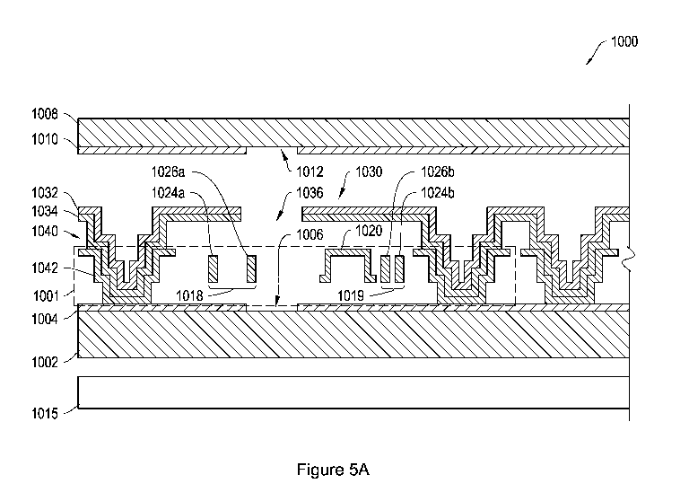
[0047] Figure 5A shows a cross-sectional view of an example display apparatus
incorporating an integrated elevated aperture layer (EAL).
[0048] Figure 5B shows a top view of an example portion of the EAL shown in
Figure 5A.
[0049] Figure 6A shows a cross-sectional view of an example display apparatus
incorporating an integrated EAL.
[0050] Figures 6B shows a top view of an example portion of the EAL shown in
Figure 6A.
[0051] Figures 6C-6E show top views of portions of additional example EALs.
[0052] Figure 7 shows a cross-sectional view of an example display apparatus
incorporating an EAL.
[0053] Figure 8 shows a cross-sectional view of a portion of an example MEMS
down
display apparatus.
[0054] Figure 9 shows a flow diagram of an example process for manufacturing a
display
apparatus.
[0055] Figures 10A-10I show cross-sectional views of stages of construction of
an example
display apparatus according to the manufacturing process shown in Figure 9.
[0056] Figure 11A shows a cross-sectional view of an example display apparatus
incorporating an encapsulated EAL.
[0057] Figures 11B-11D show cross-sectional views of stages of construction of
the
example display apparatus shown in Figure 11A.
[0058] Figure 12A shows a cross-sectional view of an example display apparatus
incorporating a ribbed EAL.
CA 02900407 2015-08-05
WO 2014/149619
PCT/US2014/019900
[0059] Figures 12B-12E show cross-sectional views of stages of construction of
the
example display apparatus shown in Figure 12A.
[0060] Figure 12F shows a cross-sectional view of an example display
apparatus.
[0061] Figures 12G-12J show plan views of example rib patterns suitable for
use in the
ribbed EALs of Figures 12A and 12E
[0062] Figure 13 shows a portion of a display apparatus incorporating an
example EAL
having light dispersion structures.
[0063] Figures 14A-14H shows top views of example portions of EALs
incorporating light
dispersion structures.
[0064] Figure 15 shows a cross-sectional view of an example display apparatus
incorporating an EAL that includes a lens structure.
[0065] Figure 16 shows a cross-sectional view of an example display apparatus
having an
EAL.
[0066] Figure 17 shows a perspective view of a portion of an example display
apparatus.
[0067] Figure 18A is a cross-sectional view of an example display apparatus.
[0068] Figures 18B and 18C show cross sectional views of additional example
display
apparatus.
[0069] Figure 19 shows a cross-sectional view of an example display apparatus.
[0070] Figures 20A and 20B show system block diagrams illustrating an example
display
device that includes a plurality of display elements.
[0071] Like reference numbers and designations in the various drawings
indicate like
elements.
DETAILED DESCRIPTION
[0072] The following description is directed to certain implementations for
the purposes of
describing the innovative aspects of this disclosure. However, a person having
ordinary skill
in the art will readily recognize that the teachings herein can be applied in
a multitude of
different ways. The described implementations may be implemented in any
device,
apparatus, or system that can be configured to display an image, whether in
motion (such as
video) or stationary (such as still images), and whether textual, graphical or
pictorial. More
11
CA 02900407 2015-08-05
WO 2014/149619
PCT/US2014/019900
particularly, it is contemplated that the described implementations may be
included in or
associated with a variety of electronic devices such as, but not limited to:
mobile telephones,
multimedia Internet enabled cellular telephones, mobile television receivers,
wireless devices,
smartphones, Bluetooth0 devices, personal data assistants (PDAs), wireless
electronic mail
receivers, hand-held or portable computers, netbooks, notebooks, smartbooks,
tablets,
printers, copiers, scanners, facsimile devices, global positioning system
(GPS)
receivers/navigators, cameras, digital media players (such as MP3 players),
camcorders,
game consoles, wrist watches, clocks, calculators, television monitors, flat
panel displays,
electronic reading devices (such as e-readers), computer monitors, auto
displays (including
odometer and speedometer displays, etc.), cockpit controls and/or displays,
camera view
displays (such as the display of a rear view camera in a vehicle), electronic
photographs,
electronic billboards or signs, projectors, architectural structures,
microwaves, refrigerators,
stereo systems, cassette recorders or players, DVD players, CD players, VCRs,
radios,
portable memory chips, washers, dryers, washer/dryers, parking meters,
packaging (such as
in electromechanical systems (EMS) applications including
microelectromechanical systems
(MEMS) applications, as well as non-EMS applications), aesthetic structures
(such as display
of images on a piece of jewelry or clothing) and a variety of EMS devices. The
teachings
herein also can be used in non-display applications such as, but not limited
to, electronic
switching devices, radio frequency filters, sensors, accelerometers,
gyroscopes, motion-
sensing devices, magnetometers, inertial components for consumer electronics,
parts of
consumer electronics products, varactors, liquid crystal devices,
electrophoretic devices,
drive schemes, manufacturing processes and electronic test equipment. Thus,
the teachings
are not intended to be limited to the implementations shown solely in the
Figures, but instead
have wide applicability as will be readily apparent to one having ordinary
skill in the art.
[0073] Certain shutter-based display apparatus can include circuits for
controlling an array
of shutter assemblies that modulate light to generate display images. The
circuits used to
control the states of the shutter assemblies can be arranged into a control
matrix. The control
matrix addresses each pixel of the array to either be in a light transmissive
state or a light
blocking state for any given image frame. In some implementations, responsive
to data
signals, the drive circuits of the control matrix selectively store actuation
voltages onto the
shutters of the shutter assemblies.
[0074] To selectively store data voltages on shutters without incurring
substantial risks of
shutter stiction, electrically isolated portions of an opposing surface are
electrically coupled
12
CA 02900407 2015-08-05
WO 2014/149619
PCT/US2014/019900
to respective shutters, such that they remain at the same potential. In some
implementations,
the shutters are electrically coupled to electrically isolated portions of a
conductive layer
disposed on an opposing substrate using compressible conductive spacers.
[0075] In some other implementations, the shutters are electrically coupled to
electrically
isolated portions of an elevated aperture layer (EAL) formed on the same
substrate as the
shutter assemblies. In some such implementations, the shutters and the EAL are
electrically
coupled by anchors used to support the shutters over the substrate. In some
other
implementations, the shutters are coupled to the EAL via separate anchors used
to the support
the EAL, but not the shutters, over the substrate on which they are
fabricated.
[0076] In some implementations, the EAL is fabricated from or includes the
same structural
materials used to form the shutter assembly. In some other implementations,
the EAL
includes a polymer encapsulated by similar structural materials. In some
implementations, a
light blocking layer is disposed on a surface of the EAL. The light blocking
layer is
reflective in some implementations, and light absorbing, in others, depending
on the
orientation of the EAL in the display apparatus. In some other
implementations, the EAL can
include light dispersing features, such as light scattering elements or
lenses, disposed across
apertures formed in the EAL.
[0077] The EAL
can be fabricated by first fabricating the shutter assemblies, and then
forming the EAL on a mold formed over the shutter assemblies. In some
implementations,
the EAL mold includes a single layer of sacrificial material. In some other
implementations,
the EAL mold is formed from multiple layers of sacrificial material. In some
such
implementations, the multiple mold layers can be used to form ribs or anti-
stiction projections
in the EAL. In some implementations, after fabrication, portions of the EAL
can be brought
into contact and adhered to an opposing substrate. Apertures are formed in the
EAL in
alignment with apertures formed in a layer of light blocking material disposed
on an
underlying substrate on which the EAL was formed.
[0078] After the EAL is fabricated, the EAL and the shutter assemblies above
which the
EAL was fabricated are released from the mold on which they were formed. To
ease the
release process, etch holes can be formed through the EAL outside of regions
of the EAL
used to prevent light leakage. In some implementations, the release process
can be facilitated
by use of a two phase etching process, in which a wet etch is used initially,
followed by a dry
etch. In some other implementations, the shutter assemblies are configured
such that
13
CA 02900407 2015-08-05
WO 2014/149619
PCT/US2014/019900
incomplete release of the mold is desired, leaving mold material to help
support the EAL or
other components over the substrate. In some other implementations, the mold
is formed
from a sacrificial material that sublimates at temperatures compatible with
thin-film
processing, thereby avoiding the need for etching.
[0079] In some implementations, one or more electrical interconnects or other
electrical
components can be formed on the EAL. In some such implementations, one of
column or
row interconnects can be formed on top of the EAL, while the other of column
or row
interconnects can be formed on the underlying substrate. In some
implementations, electrical
components such as transistors, capacitors, diodes, or other electrical
components also can be
formed on the surface of the EAL.
[0080] Particular implementations of the subject matter described in this
disclosure can be
implemented to realize one or more of the following potential advantages. In
general, the use
of an EAL provides manufacturing advantages, optical advantages, and display
element
control advantages.
[0081] With respect to manufacturing advantages, the use of an EAL enables the
fabrication of substantially all electromechanical and optical components of a
display on a
single substrate. This substantially increases the alignment tolerances
between the substrates,
and in some implementations can virtually eliminate the need to align the
substrates. In
addition, the inclusion of the EAL obviates the need to form an electrical
connection between
individual display elements on one substrate and respective regions of the
other substrate.
This allows the two substrates to be fabricated further apart, limiting and in
some
implementations the need to form spacers between the two substrates. This
extra space also
allows a front substrate to deform in response to temperature changes,
alleviating the need for
fabricating alternative bubble reduction or mitigation features within the
display. In addition,
the EAL does not need to deform in response to temperature changes, keeping
the apertures a
substantially constant distance from a rear substrate. This substantially
constant distance
helps maintain viewing angle performance for the display, which can be
disturbed by aperture
layer deformation. Furthermore, the additional space may reduce the likelihood
of cavitation
bubble formation resulting from impacts on the surface of the display, which
can damage the
display elements.
[0082] In some implementations, the EAL can be fabricated using two mold
layers. Doing
so allows the EAL to include anti-stiction projections or stiffening ribs. The
former helps
14
CA 02900407 2015-08-05
WO 2014/149619
PCT/US2014/019900
mitigate the risk of display elements adhering to the EAL. The latter helps
strengthen the
EAL against external pressures. In some other implementations, an EAL can be
strengthened
by having it enclose a layer of polymer material.
[0083] With respect to optics, the use of an EAL can improve the viewing angle
characteristics of a display. A display can include a pair of opposing
apertures that form a
portion of optical path from a backlight to viewer to be located closer
together. The distance
between such apertures can limit the viewing angle of the display. Using an
EAL can allow
the opposing apertures to be placed closer to one another, thereby improving
viewing angle
characteristics. In addition, optical structures can be fabricated on top of
apertures defined by
an EAL. These structures can disperse light, further improving viewing angle
characteristics
of the display.
[0084] In some implementations, the EAL can be fabricated such that it is
supported by
some of the same anchors that support portions of display elements over a
substrate. This
reduces the number of structures needed to support the EAL, freeing additional
room for
electrical, mechanical, or optical components, including additional display
elements in higher
pixel-per-inch (PPI) displays. Such a configuration also provides a ready
means for
electrically linking portions of individual display elements to respective
isolated conductive
regions formed on the EAL. These display element-specific electrical
connections permit
alternative control circuit configurations. For example, in some such
implementations, the
circuits that control the states of the display elements provide a varying
actuation voltage to
portions of different display elements, instead of maintaining such portions
at a common
voltage across display elements. Such control circuits can be faster to
actuate, require less
space, and have higher reliability.
[0085] In some other implementations, certain components of the control
circuits (also
referred to as a control matrix), can be fabricated on top of the EAL, as
opposed to on the
surface of the substrate. For example, some interconnects included in the
control matrix can
be fabricated on top of the EAL, while other interconnects are formed on the
substrate.
Separating interconnects in such a fashion reduces the parasitic capacitance
between
interconnects. Other electronic components such as transistors or capacitors
also can be built
on the EAL. The extra real estate resulting from moving the electronics to the
top of the EAL
allows for higher aperture ratio displays, or higher resolution displays with
smaller display
elements.
CA 02900407 2015-08-05
WO 2014/149619
PCT/US2014/019900
[0086] As described above, various techniques can be employed to facilitate
release of
display elements fabricated below an EAL. For example, etch holes through the
EAL can
provide additional fluid pathways for etchants to reach the sacrificial mold
on which the
display elements and the EAL are built. This reduces the time required for
release, thereby
improving overall manufacturing efficiency while also limiting the exposure of
the display
elements and the EAL to potentially corrosive etchants, which could damage the
display
elements, thereby reducing their manufacturing yield or long-term durability.
Such exposure
also can be limited by employing a two-phase etching process. In some
implementations,
such exposure can be limited further by employing a sublimatable sacrificial
mold. Doing so
also reduces to need to form additional fluid paths through the EAL to ensure
chemical
etchants reach the sacrificial material in a timely fashion. In addition,
designs that
intentionally allow for the incomplete removal of the sacrificial mold can
result in stronger
display element anchors, yielding a more durable display.
[0087] Figure lA shows a schematic diagram of an example direct-view
microelectromechanical system (MEMS)-based display apparatus 100. The display
apparatus
100 includes a plurality of light modulators 102a-102d (generally "light
modulators 102")
arranged in rows and columns. In the display apparatus 100, the light
modulators 102a and
102d are in the open state, allowing light to pass. The light modulators 102b
and 102c are in
the closed state, obstructing the passage of light. By selectively setting the
states of the light
modulators 102a-102d, the display apparatus 100 can be utilized to form an
image 104 for a
backlit display, if illuminated by a lamp or lamps 105. In another
implementation, the
apparatus 100 may form an image by reflection of ambient light originating
from the front of
the apparatus. In another implementation, the apparatus 100 may form an image
by reflection
of light from a lamp or lamps positioned in the front of the display, i.e., by
use of a front
light.
[0088] In some implementations, each light modulator 102 corresponds to a
pixel 106 in the
image 104. In some other implementations, the display apparatus 100 may
utilize a plurality
of light modulators to form a pixel 106 in the image 104. For example, the
display apparatus
100 may include three color-specific light modulators 102. By selectively
opening one or
more of the color-specific light modulators 102 corresponding to a particular
pixel 106, the
display apparatus 100 can generate a color pixel 106 in the image 104. In
another example,
the display apparatus 100 includes two or more light modulators 102 per pixel
106 to provide
16
CA 02900407 2015-08-05
WO 2014/149619
PCT/US2014/019900
luminance level in an image 104. With respect to an image, a "pixel"
corresponds to the
smallest picture element defined by the resolution of image. With respect to
structural
components of the display apparatus 100, the term "pixel" refers to the
combined mechanical
and electrical components utilized to modulate the light that forms a single
pixel of the
image.
[0089] The display apparatus 100 is a direct-view display in that it may not
include imaging
optics typically found in projection applications. In a projection display,
the image formed
on the surface of the display apparatus is projected onto a screen or onto a
wall. The display
apparatus is substantially smaller than the projected image. In a direct view
display, the user
sees the image by looking directly at the display apparatus, which contains
the light
modulators and optionally a backlight or front light for enhancing brightness
and/or contrast
seen on the display.
[0090] Direct-view displays may operate in either a transmissive or reflective
mode. In a
transmissive display, the light modulators filter or selectively block light
which originates
from a lamp or lamps positioned behind the display. The light from the lamps
is optionally
injected into a lightguide or "backlight" so that each pixel can be uniformly
illuminated.
Transmissive direct-view displays are often built onto transparent or glass
substrates to
facilitate a sandwich assembly arrangement where one substrate, containing the
light
modulators, is positioned directly on top of the backlight.
[0091] Each light modulator 102 can include a shutter 108 and an aperture 109.
To
illuminate a pixel 106 in the image 104, the shutter 108 is positioned such
that it allows light
to pass through the aperture 109 towards a viewer. To keep a pixel 106 unlit,
the shutter 108
is positioned such that it obstructs the passage of light through the aperture
109. The aperture
109 is defined by an opening patterned through a reflective or light-absorbing
material in
each light modulator 102.
[0092] The display apparatus also includes a control matrix connected to the
substrate and
to the light modulators for controlling the movement of the shutters. The
control matrix
includes a series of electrical interconnects (e.g., interconnects 110, 112
and 114), including
at least one write-enable interconnect 110 (also referred to as a "scan-line
interconnect") per
row of pixels, one data interconnect 112 for each column of pixels, and one
common
interconnect 114 providing a common voltage to all pixels, or at least to
pixels from both
17
CA 02900407 2015-08-05
WO 2014/149619
PCT/US2014/019900
multiple columns and multiples rows in the display apparatus 100. In response
to the
application of an appropriate voltage (the "write-enabling voltage, VwE"), the
write-enable
interconnect 110 for a given row of pixels prepares the pixels in the row to
accept new shutter
movement instructions. The data interconnects 112 communicate the new movement
instructions in the form of data voltage pulses. The data voltage pulses
applied to the data
interconnects 112, in some implementations, directly contribute to an
electrostatic movement
of the shutters. In some other implementations, the data voltage pulses
control switches, such
as, transistors or other non-linear circuit elements that control the
application of separate
actuation voltages, which are typically higher in magnitude than the data
voltages, to the light
modulators 102. The application of these actuation voltages then results in
the electrostatic
driven movement of the shutters 108.
[0093] Figure 1B shows a block diagram 120 of an example host device (i.e.,
cell phone,
smart phone, PDA, MP3 player, tablet, e-reader, etc.). The host device
includes a display
apparatus 128, a host processor 122, environmental sensors 124, a user input
module 126, and
a power source.
[0094] The display apparatus 128 includes a plurality of scan drivers 130
(also referred to
as "write enabling voltage sources"), a plurality of data drivers 132 (also
referred to as "data
voltage sources"), a controller 134, common drivers 138, lamps 140-146, and
lamp drivers
148. The scan drivers 130 apply write enabling voltages to write-enable
interconnects 110.
The data drivers 132 apply data voltages to the data interconnects 112.
[0095] In some implementations of the display apparatus, the data drivers 132
are
configured to provide analog data voltages to the light modulators, especially
where the
luminance level of the image 104 is to be derived in analog fashion. In analog
operation, the
light modulators 102 are designed such that when a range of intermediate
voltages is applied
through the data interconnects 112, there results a range of intermediate open
states in the
shutters 108 and therefore a range of intermediate illumination states or
luminance levels in
the image 104. In other cases, the data drivers 132 are configured to apply
only a reduced set
of 2,3 or 4 digital voltage levels to the data interconnects 112. These
voltage levels are
designed to set, in digital fashion, an open state, a closed state, or other
discrete state to each
of the shutters 108.
18
CA 02900407 2015-08-05
WO 2014/149619
PCT/US2014/019900
[0096] The scan drivers 130 and the data drivers 132 are connected to a
digital controller
circuit 134 (also referred to as the "controller 134"). The controller sends
data to the data
drivers 132 in a mostly serial fashion, organized in sequences, which in some
implementations may be predetermined, grouped by rows and by image frames. The
data
drivers 132 can include series to parallel data converters, level shifting,
and for some
applications digital to analog voltage converters.
[0097] The display apparatus optionally includes a set of common drivers 138,
also referred
to as common voltage sources. In some implementations, the common drivers 138
provide a
DC common potential to all light modulators within the array of light
modulators, for
instance by supplying voltage to a series of common interconnects 114. In some
other
implementations, the common drivers 138, following commands from the
controller 134,
issue voltage pulses or signals to the array of light modulators, for instance
global actuation
pulses which are capable of driving and/or initiating simultaneous actuation
of all light
modulators in multiple rows and columns of the array.
[0098] All of the drivers (e.g., scan drivers 130, data drivers 132 and common
drivers 138)
for different display functions are time-synchronized by the controller 134.
Timing
commands from the controller coordinate the illumination of red, green and
blue and white
lamps (140, 142, 144 and 146 respectively) via lamp drivers 148, the write-
enabling and
sequencing of specific rows within the array of pixels, the output of voltages
from the data
drivers 132, and the output of voltages that provide for light modulator
actuation.
[0099] The controller 134 determines the sequencing or addressing scheme by
which each
of the shutters 108 can be re-set to the illumination levels appropriate to a
new image 104.
New images 104 can be set at periodic intervals. For instance, for video
displays, the color
images 104 or frames of video are refreshed at frequencies ranging from 10 to
300 Hertz
(Hz). In some implementations the setting of an image frame to the array is
synchronized
with the illumination of the lamps 140, 142, 144 and 146 such that alternate
image frames are
illuminated with an alternating series of colors, such as red, green and blue.
The image
frames for each respective color is referred to as a color subframe. In this
method, referred to
as the field sequential color method, if the color subframes are alternated at
frequencies in
excess of 20 Hz, the human brain will average the alternating frame images
into the
perception of an image having a broad and continuous range of colors. In
alternate
19
CA 02900407 2015-08-05
WO 2014/149619
PCT/US2014/019900
implementations, four or more lamps with primary colors can be employed in
display
apparatus 100, employing primaries other than red, green and blue.
[0100] In some implementations, where the display apparatus 100 is designed
for the digital
switching of shutters 108 between open and closed states, the controller 134
forms an image
by the method of time division gray scale, as previously described. In some
other
implementations, the display apparatus 100 can provide gray scale through the
use of
multiple shutters 108 per pixel.
[0101] In some implementations, the data for an image state 104 is loaded by
the controller
134 to the modulator array by a sequential addressing of individual rows, also
referred to as
scan lines. For each row or scan line in the sequence, the scan driver 130
applies a write-
enable voltage to the scan-line interconnect 110 for that row of the array,
and subsequently
the data driver 132 supplies data voltages, corresponding to desired shutter
states, for each
column in the selected row. This process repeats until data has been loaded
for all rows in
the array. In some implementations, the sequence of selected rows for data
loading is linear,
proceeding from top to bottom in the array. In some other implementations, the
sequence of
selected rows is pseudo-randomized, in order to minimize visual artifacts. And
in some other
implementations, the sequencing is organized by blocks, where, for a block,
the data for only
a certain fraction of the image state 104 is loaded to the array, for instance
by addressing only
every 5th row of the array in sequence.
[0102] In some implementations, the process for loading image data to the
array is
separated in time from the process of actuating the shutters 108. In these
implementations,
the modulator array may include data memory elements for each pixel in the
array and the
control matrix may include a global actuation interconnect for carrying
trigger signals, from
common driver 138, to initiate simultaneous actuation of shutters 108
according to data
stored in the memory elements.
[0103] In alternative implementations, the array of pixels and the control
matrix that
controls the pixels may be arranged in configurations other than rectangular
rows and
columns. For example, the pixels can be arranged in hexagonal arrays or
curvilinear rows
and columns. In general, as used herein, the term scan-line shall refer to any
plurality of
pixels that share a write-enabling interconnect.
CA 02900407 2015-08-05
WO 2014/149619
PCT/US2014/019900
[0104] The host processor 122 generally controls the operations of the host.
For example,
the host processor may be a general or special purpose processor for
controlling a portable
electronic device. With respect to the display apparatus 128, included within
the host device
120, the host processor outputs image data as well as additional data about
the host. Such
information may include data from environmental sensors, such as ambient light
or
temperature; information about the host, including, for example, an operating
mode of the
host or the amount of power remaining in the host's power source; information
about the
content of the image data; information about the type of image data; and/or
instructions for
display apparatus for use in selecting an imaging mode.
[0105] The user input module 126 conveys the personal preferences of the user
to the
controller 134, either directly, or via the host processor 122. In some
implementations, the
user input module is controlled by software in which the user programs
personal preferences
such as "deeper color," "better contrast," "lower power," "increased
brightness," "sports,"
"live action," or "animation." In some other implementations, these
preferences are input to
the host using hardware, such as a switch or dial. The plurality of data
inputs to the controller
134 direct the controller to provide data to the various drivers 130, 132, 138
and 148 which
correspond to optimal imaging characteristics.
[0106] An environmental sensor module 124 also can be included as part of the
host device.
The environmental sensor module receives data about the ambient environment,
such as
temperature and or ambient lighting conditions. The sensor module 124 can be
programmed
to distinguish whether the device is operating in an indoor or office
environment versus an
outdoor environment in bright daylight versus and outdoor environment at
nighttime. The
sensor module communicates this information to the display controller 134, so
that the
controller can optimize the viewing conditions in response to the ambient
environment.
[0107] Figure 2 shows a perspective view of an illustrative shutter-based
light modulator
200. The shutter-based light modulator is suitable for incorporation into the
direct-view
MEMS-based display apparatus 100 of Figure 1A. The light modulator 200
includes a
shutter 202 coupled to an actuator 204. The actuator 204 can be formed from
two separate
compliant electrode beam actuators 205 (the "actuators 205"). The shutter 202
couples on
one side to the actuators 205. The actuators 205 move the shutter 202
transversely over a
substrate 203 in a plane of motion which is substantially parallel to the
substrate 203. The
21
CA 02900407 2015-08-05
WO 2014/149619
PCT/US2014/019900
opposite side of the shutter 202 couples to a spring 207 which provides a
restoring force
opposing the forces exerted by the actuator 204.
[0108] Each actuator 205 includes a compliant load beam 206 connecting the
shutter 202 to
a load anchor 208. The load anchors 208 along with the compliant load beams
206 serve as
mechanical supports, keeping the shutter 202 suspended proximate to the
substrate 203. The
surface includes one or more aperture holes 211 for admitting the passage of
light. The load
anchors 208 physically connect the compliant load beams 206 and the shutter
202 to the
substrate 203 and electrically connect the load beams 206 to a bias voltage,
in some
instances, ground.
[0109] If the substrate is opaque, such as silicon, then aperture holes 211
are formed in the
substrate by etching an array of holes through the substrate 204. If the
substrate 204 is
transparent, such as glass or plastic, then the aperture holes 211 are formed
in a layer of light-
blocking material deposited on the substrate 203. The aperture holes 211 can
be generally
circular, elliptical, polygonal, serpentine, or irregular in shape.
[0110] Each actuator 205 also includes a compliant drive beam 216 positioned
adjacent to
each load beam 206. The drive beams 216 couple at one end to a drive beam
anchor 218
shared between the drive beams 216. The other end of each drive beam 216 is
free to move.
Each drive beam 216 is curved such that it is closest to the load beam 206
near the free end of
the drive beam 216 and the anchored end of the load beam 206.
[0111] In operation, a display apparatus incorporating the light modulator 200
applies an
electric potential to the drive beams 216 via the drive beam anchor 218. A
second electric
potential may be applied to the load beams 206. The resulting potential
difference between
the drive beams 216 and the load beams 206 pulls the free ends of the drive
beams 216
towards the anchored ends of the load beams 206, and pulls the shutter ends of
the load
beams 206 toward the anchored ends of the drive beams 216, thereby driving the
shutter 202
transversely towards the drive beam anchor 218. The compliant load beams 206
act as
springs, such that when the voltage across the beams 206 and 216 potential is
removed, the
load beams 206 push the shutter 202 back into its initial position, releasing
the stress stored in
the load beams 206.
[0112] A light modulator, such as the light modulator 200, incorporates a
passive restoring
force, such as a spring, for returning a shutter to its rest position after
voltages have been
22
CA 02900407 2015-08-05
WO 2014/149619
PCT/US2014/019900
removed. Other shutter assemblies can incorporate a dual set of "open" and
"closed"
actuators and separate sets of "open" and "closed" electrodes for moving the
shutter into
either an open or a closed state.
[0113] There are a variety of methods by which an array of shutters and
apertures can be
controlled via a control matrix to produce images, in many cases moving
images, with
appropriate luminance levels. In some cases, control is accomplished by means
of a passive
matrix array of row and column interconnects connected to driver circuits on
the periphery of
the display. In other cases, it is appropriate to include switching and/or
data storage elements
within each pixel of the array (the so-called active matrix) to improve the
speed, the
luminance level and/or the power dissipation performance of the display.
[0114] Figures 3A and 3B show portions of two example control matrices 800 and
860. As
described above, a control matrix is a collection of interconnects and
circuitry used to address
and actuate the display elements of a display. In some implementations, the
control matrix
800 can be implemented for use in the display apparatus 100 shown in Figure 1B
and is
formed using thin-film components, such as thin-film transistors (TFTs) and
other thin film
components.
[0115] The control matrix 800 controls an array of pixels 802, a scan-line
interconnect 806
for each row of pixels 802, a data interconnect 808 for each column of pixels
802, and
several common interconnects that each carry signals to multiple rows and
multiple columns
of pixels at the same time. The common interconnects include an actuation
voltage
interconnect 810, a global update interconnect 812, a common drive
interconnect 814, and a
shutter common interconnect 816.
[0116] Each pixel in the control matrix includes a light modulator 804, a data
storage
circuit 820, and an actuation circuit 825. The light modulator 804 includes a
first actuator
805a and a second actuator 805b (generally "actuators 805") for moving a light
obstructing
component, such as a shutter807, between at least an obstructive and a non-
obstructive state.
In some implementations, the obstructive state corresponds to a light
absorbing dark state in
which the shutter 807 obstructs the path of light from a backlight out towards
and through the
front of the display to a viewer. The non-obstructive state can correspond to
a transmissive
or light state, in which the shutter 807 is outside of the path of light,
allowing the light
emitted by the backlight to be output through the front of the display. In
some other
23
CA 02900407 2015-08-05
WO 2014/149619
PCT/US2014/019900
implementations, the obstructive state is a reflective state and the non-
obstructive state is a
light absorbing state.
[0117] The data storage circuit 820 also includes a write-enabling transistor
830, and a data
storage capacitor 835. The data storage circuit 820 is controlled by the scan-
line interconnect
806 and the data interconnect 808. More particularly, the scan-line
interconnect 806
selectively allows data to be loaded into the pixels 802 of a row by supplying
a voltage to the
gates of the write-enabling transistors 830 of the respective pixel actuation
circuits 825. The
data interconnect 808 provides a data voltage corresponding to the data to be
loaded into the
pixel 802 of its corresponding column in the row for which the scan-line
interconnect 806 is
active. To that end, the data interconnect 808 couples the source of the write-
enabling
transistor 830. The drain of the write-enabling transistor 830 couples to the
data storage
capacitor 835. If the scan-line interconnect 806 is active, a data voltage
applied to the data
interconnect 808 passes through the write-enabling transistor 830 and is
stored on the data
storage capacitor 835.
[0118] The pixel actuation circuit 825 includes an update transistor 840 and a
charge
transistor 845. The gate of the update transistor 840 is coupled to the data
storage capacitor
835 and the drain of the write-enable transistor 830. The drain of the update
transistor 840 is
coupled to the global update interconnect 812. The source of the update
transistor 840 is
coupled to the drain of the charge transistor 845 and a first active node 852,
which is coupled
to a drive electrode 809a of the first actuator 805a. The gate and source of
the charge
transistor 845 are connected to the actuation voltage interconnect 810.
[0119] A drive electrode 809b of the second actuator 805b is coupled to the
common drive
interconnect 814 at a second active node 854. The shutter 807 also is coupled
to the shutter
common interconnect 816, which in some implementations, is maintained at
ground. The
shutter common interconnect 816 is configured to be coupled to each of the
shutters in the
array of pixels 802. In this way, all of the shutters are maintained at the
same voltage
potential.
[0120] The control matrix 800 can operate in three general stages. First, data
voltages for
pixels in a display are loaded for each pixel one row at a time in a data
loading stage. Next,
in a precharge stage, the common drive interconnect 814 is grounded and
actuation voltage
interconnect 810 is brought high. Doing so lowers the voltage on the drive
electrode 809b of
24
CA 02900407 2015-08-05
WO 2014/149619
PCT/US2014/019900
the second actuators 805b of the pixels and applies a high voltage to the
drive electrodes 809a
of the first actuators 805a of the pixels 802. This results in all of the
shutters 807 moving
towards the first actuator 805, if they were not already in that position.
Next, in a global
update stage, the pixels 802 are moved (if necessary) to the state indicated
by the data voltage
loaded into the pixels 802 in the data loading stage.
[0121] The data loading stage proceeds with applying a write-enabling voltage
Võ to a first
row of the array of pixels 802 via the scan-line interconnect 806. As
described above, the
application of a write-enabling voltage V, to the scan-line interconnect 806
corresponding to
a row turns on the write-enable transistors 830 of all pixels 802 in that row.
Then a data
voltage is applied to each data interconnect 808. The data voltage can be
high, such as
between about 3V and about 7V, or it can be low, for example, at or about
ground. The data
voltage on each data interconnect 808 is stored on the data storage capacitor
835 of its
respective pixel in the write-enabled row.
[0122] Once all the pixels 802 in the row are addressed, the control matrix
800 removes the
write-enabling voltage Vwe from the scan-line interconnect 806. In some
implementations,
the control matrix 800 grounds the scan-line interconnect 806. The data
loading stage is then
repeated for subsequent rows of the array in the control matrix 800. At the
end of the data
loading sequence, each of the data storage capacitors 835 in the selected
group of pixels 802
stores the data voltage which is appropriate for the setting of the next image
state.
[0123] The control matrix 800 then proceeds with the precharge stage. In the
precharge
stage, in each pixel 802, the drive electrode 809a of the first actuator 805a
is charged to the
actuation voltage, and the drive electrode 809b of the second actuator 805b is
grounded. If
the shutter 807 in the pixel 802 was not already moved towards the first
actuator 805a for the
previous image, then this process causes the shutter 807 to do so. The
precharge stage begins
by providing an actuation voltage to the actuation voltage interconnect 810
and providing a
high voltage at the global update interconnect 812. The actuation voltage, in
some
implementations, can be between about 20V and about 50V. The high voltage
applied to the
global update interconnect 812 can be between about 3V and about 7V. By doing
so, the
actuation voltage from the actuation voltage interconnect 810 can pass through
the charge
transistor 845, bringing the first active node 852 and the drive electrode
809a of the first
actuator 805a up to the actuation voltage. As a result, the shutter 807 either
remains attracted
to the first actuator 805a or moves towards the first actuator from the second
actuator 805b.
CA 02900407 2015-08-05
WO 2014/149619
PCT/US2014/019900
[0124] The control matrix 800 then activates the common drive interconnect
814. This
brings the second active node 854 and the drive electrode 809b of the second
actuator 805b to
the actuation voltage. The actuation voltage interconnect 810 is then brought
down to a low
voltage, such as ground. At this stage, the actuation voltage is stored on the
drive electrodes
809a and 809b of both actuators 805. However, as the shutter 807 is already
moved towards
the first actuator 805a, it remains in that position unless and until the
voltage on the drive
electrode 809a of the first actuator is brought down. The control matrix 800
then waits a
sufficient amount of time for all of the shutters 807 to reliably have reached
their positions
adjacent the first actuator 805a before proceeding.
[0125] Next, the control matrix 800 proceeds with the update stage. In this
stage, the global
update interconnect 812 is brought to a low voltage. Bringing the global
update interconnect
812 down enables the update transistor 840 to respond to the data voltage
stored on the data
storage capacitor 835. Depending on the voltage of the data voltage stored at
the data storage
capacitor 835, the update transistor 840 will either switch ON or remain
switched OFF. If the
data voltage stored at the data storage capacitor 835 is high, the update
transistor 840
switches ON, resulting in the voltage at the first active node 852 and on the
drive electrode
809a of the first actuator 805a to collapse to ground. As the voltage on the
drive electrode
809b of the second actuator 805b remains high, the shutter 807 moves towards
the second
actuator 805b. Conversely, if the data voltage stored in the data storage
capacitor 835 is low,
the update transistor 840 remains switched OFF. As a result, the voltage at
the first active
node 852 and on the drive electrode 809a of the first actuator 805a remains at
the actuation
voltage level, keeping the shutter in place. After enough time has passed to
ensure all
shutters 807 have reliably travelled to their intended positions, the display
can illuminate its
backlight to display the image resulting from the shutter states loaded into
the array of pixels
802.
[0126] In the process described above, for each set of pixel states the
control matrix 800
displays, the control matrix 800 takes at least twice the time needed for the
shutter 807 to
travel between states in order to ensure the shutter 807 ends up in the proper
position. That
is, all the shutters 807 are first brought towards the first actuator 805a,
requiring one shutter
travel time, before they are then selectively allowed to move towards the
second actuator
805b, requiring a second shutter travel time. If the global update stage
commences too
26
CA 02900407 2015-08-05
WO 2014/149619
PCT/US2014/019900
quickly, the shutter 807 may not have enough time to reach the first actuator
805a. As a
result, the shutter may move towards the incorrect state during the global
update stage.
[0127] In contrast to shutter-based display circuits, such as the control
matrix 800 shown in
Figure 3A, in which the shutters are maintained at a common voltage and are
driven by
varying the voltage applied to the drive electrodes 809a and 809b of opposing
actuators 805a
and 805b, a display circuit in which the shutter is itself coupled to an
active node can be
implemented. Shutters controlled by such a circuit can be directly driven into
their respective
desired states without first all having to be moved into a common position, as
described with
respect to the control matrix 800. As a result, such a circuit requires less
time to address and
actuate, and reduces the risk of shutters not correctly entering their desired
states.
[0128] Figure 3B shows a portion of a control matrix 860. The control matrix
860 is
configured to selectively apply actuation voltages to the load electrode 811
of each actuator
805, instead of to the drive electrode 809. The load electrodes 811 are
directly coupled to the
shutter 807. This is in contrast to the control matrix 800 depicted in Figure
3A, in which the
shutter 807 was kept at a constant voltage.
[0129] Similar to the control matrix 800 shown in Figure 3A, the control
matrix 860 can be
implemented for use in the display apparatus 100 shown in Figures lA and 1B.
In some
implementations, the control matrix 860 also can be implemented for use in the
display
apparatus shown in Figures 4, 5A, 7, 8 and 13-18, described below. The
structure of the
control matrix 860 is described immediately below.
[0130] Like the control matrix 800, the control matrix 860 controls an array
of pixels 862.
Each pixel 862 includes a light modulator 804. Each light modulator includes a
shutter 807.
The shutter 807 is driven by actuators 805a and 805b between a position
adjacent the first
actuator 805a and a position adjacent the second actuator 805b. Each actuator
805a and 805b
includes a load electrode 811 and a drive electrode 809. Generally, as used
herein, a load
electrode 811 of an electrostatic actuator corresponds to the electrode of the
actuator coupled
to the load being moved by the actuator. Accordingly, with respect to the
actuators 805a and
805b, the load electrode 811 refers to an electrode of the actuator that
couples to the shutter
807. The drive electrode 809 refers to the electrode paired with and opposing
the load
electrode 811 to form the actuator.
27
CA 02900407 2015-08-05
WO 2014/149619
PCT/US2014/019900
[0131] The control matrix 860 includes a data loading circuit 820 similar to
that of the
control matrix 800. The control matrix 860, however, includes different common
interconnects than the control matrix 800 and a significantly different
actuation circuit 861.
[0132] The control matrix 860 includes three common interconnects which were
not
included in the control matrix 800 of Figure 3A. Specifically, the control
matrix 860 includes
a first actuator drive interconnect 872, a second actuator drive interconnect
874, and a
common ground interconnect 878. In some implementations, the first actuator
drive
interconnect 872 is maintained at a high voltage and the second actuator drive
interconnect
874 is maintained at a low voltage. In some other implementations, the
voltages are reversed,
i.e., the first actuator drive interconnect is maintained at a low voltage and
the second
actuator drive interconnect 874 is maintained at a high voltage. While the
following
description of the control matrix 860 assumes a constant voltage being applied
to the first and
second actuator drive interconnects 872 and 874 (as set forth above), in some
other
implementations, the voltages on the first actuator drive interconnect 872 and
the second
actuator drive interconnects 874, as well as the input data voltage, are
periodically reversed to
avoid charge build-up on the electrodes of the actuators 805 and 805b.
[0133] The common ground interconnect 878 serves merely to provide a reference
voltage
for data stored on the data storage capacitor 835. In some implementations,
the control
matrix 860 can forego the common ground interconnect 878, and instead have the
data
storage capacitor coupled to the first or second actuator drive interconnect
872 and 874. The
function of the actuator drive interconnects 872 and 874 is described further
below.
[0134] Like the control matrix 800, the actuation circuit 861 of the control
matrix 860
includes an update transistor 840 and a charge transistor 845. In contrast,
however, the
charge transistor 845 and the update transistor 840 are coupled to the load
electrode 811 of
the first actuator 805a of the light modulator 804, instead of the drive
electrode 809a of the
first actuator 805a. As a result, when the charge transistor 845 is activated,
an actuation
voltage is stored on the load electrodes 811 of both of the actuators 805a and
805b, as well as
on the shutter 807. Thus, the update transistor 840, instead of selectively
discharging the
drive electrodes 809a of the first actuator 805a, based on image data stored
on the storage
capacitor 835, selectively discharges the load electrodes 811 of the actuators
805a and 805b
and the shutter 807, removing the potential on the components.
28
CA 02900407 2015-08-05
WO 2014/149619
PCT/US2014/019900
[0135] As indicated above, the first actuator drive interconnect 872 is
maintained at a high
voltage and the second actuator drive interconnect 874 is maintained at a low
voltage.
Accordingly, while an actuation voltage is stored on the shutter 807 and the
load electrodes
811 of the actuators 805a and 805b, the shutter 807 moves to the second
actuator 805b,
whose drive electrode 809b is maintained at a low voltage. When the shutter
807 and the
load electrodes 811 of the actuators 805a and 805b are brought low, the
shutter 807 moves
towards the first actuator 805a, whose drive electrode 809a is maintained at a
high voltage.
01361 The control matrix 860 can operate in two general stages. First, data
voltages for
pixels 862 in a display are loaded for each pixel 862, one or more rows at a
time, in a data
loading stage. The data voltages are loaded in a manner similar to that
described above with
respect to Figure 3A. In addition, the global update interconnect 812 is
maintained at a high
voltage potential to prevent the update transistor 840 from switching ON
during the data
loading stage.
[0137] After the data loading stage is complete, the shutter actuation stage
begins by
providing an actuation voltage to the actuation voltage interconnect 810. By
providing the
actuation voltage to the actuation voltage interconnect 810, the charge
transistor 845 is
switched ON allowing the current to flow through the charge transistor 845,
bringing the
shutter 807 up to about the actuation voltage. After a sufficient period of
time has passed to
allow the actuation voltage to be stored on the shutter 807, the actuation
voltage interconnect
810 is brought low. The amount of time needed for this to occur is
substantially less than the
time needed for a shutter 807 to change states. The update interconnect 812 is
brought low
immediately thereafter. Depending on the data voltage stored at the data
storage capacitor
835, the update transistor 840 will either remain OFF or will switch ON.
[0138] If the data voltage is high, the update transistor 840 switches ON,
discharging the
shutter 807 and the load electrodes 811of the actuators 805a and 805b. As a
result, the
shutter is attracted to the first actuator 805a. Conversely, if the data
voltage is low, the
update transistor 840 remains OFF. As a result, the actuation voltage remains
on the shutter
and the load electrodes 811 of the actuators 805a and 805b. The shutter, as a
result is
attracted to the second actuator 805b.
[0139] Due to the architecture of the actuation circuit 861, it is permissible
for the shutter
807 to be in any state, even an indeterminate state, when the update
transistor 840 is turned
29
CA 02900407 2015-08-05
WO 2014/149619
PCT/US2014/019900
ON. This enables the immediate switching of the update transistor 840 as
soon as the
actuation voltage interconnect 810 is brought low. In contrast to the
operation of the control
matrix 800, with the control matrix 860, no time needs to be set aside to
allow the shutter 807
to move to any particular state. Moreover, because the initial state of the
shutter 807 has little
to no impact on its final state, the risk of a shutter 807 entering the wrong
state is
substantially reduced.
[0140] Shutter assemblies employing control matrices similar to the control
matrix 800
depicted in Figure 3A face the risk of their respective shutters being drawn
towards an
opposing substrate due to charge build up on the substrate. If the charge
build-up is
sufficiently large, the resulting electrostatic forces can draw the shutter
into contact with the
opposing substrate, where it can sometimes permanently adhere due to stiction.
To reduce
this risk, a substantially continuous conductive layer can be deposited across
the surface of
the opposing substrate to dissipate the charge that might otherwise build up.
In some
implementations, such a conductive layer can be electrically coupled to the
shutter common
interconnect 816 of the control matrix 800 (as shown in Figure 3A) to help
keep the shutters
807 and the conductive layer at a common potential.
[0141] Shutter assemblies employing control matrices similar to the control
matrix 860 of
Figure 3B bear additional risk of shutter stiction to an opposing substrate.
The risk to such
shutter assemblies, cannot, however, be mitigated by use of a similar
substantially continuous
conductive layer being deposited on the opposing substrate. In using a control
matrix similar
to the control matrix 860, shutters are driven to different voltages at
different times. Thus at
any given time, if the opposing substrate were kept at a common potential,
some shutters
would experience little electrostatic force, while others would experience
large electrostatic
forces.
[0142] Thus, to implement a display apparatus using a control matrix similar
to the control
matrix 860 shown in Figure 3B, the display apparatus can incorporate a
pixilated conductive
layer. Such a conductive layer is divided into multiple electrically isolated
regions, with each
region corresponding to, and being electrically coupled to, the shutter of a
vertically adjacent
shutter assembly. One display apparatus architecture suitable for use with a
control matrix
similar to the control matrix 860 depicted in Figure 3B is shown in Figure 4.
CA 02900407 2015-08-05
WO 2014/149619
PCT/US2014/019900
[0143] Figure 4 shows a cross-sectional view of an example display apparatus
900
incorporating flexible conductive spacers. The display apparatus 900 is built
in a MEMS-up
configuration. That is, an array of shutter-based display elements that
includes a plurality of
shutters 920 is fabricated on a transparent substrate 910 positioned towards
the rear of the
display apparatus 900 and faces up towards a cover sheet 940 that forms the
front of the
display apparatus 900. The transparent substrate 910 is coated with a light
absorbing layer
912 through which rear apertures 914 corresponding to the overlying shutters
920 are formed.
The transparent substrate 910 is positioned in front of a backlight 950. Light
emitted by the
backlight 950 passes through the apertures 914 to be modulated by the shutters
920.
[0144] The display elements include anchors 904 configured to support one or
more
electrodes, such as drive electrodes 924 and load electrodes 926 that make up
the actuators of
the display apparatus 900.
[0145] The display apparatus 900 also includes a cover sheet 940 on which a
conductive
layer 922 is formed. The conductive layer 922 is pixilated to form a plurality
of electrically
isolated conductive regions that correspond to respective ones of the
underlying shutters 920.
Each of the electrically isolated conductive regions formed on the cover sheet
940 is
vertically adjacent to an underlying shutter 920 and is electrically coupled
thereto. The cover
sheet 940 further includes a light blocking layer 942 through which a
plurality of front
apertures 944 are formed. The front apertures 944 are aligned with the rear
apertures 914
formed through the light absorbing layer 912 on the transparent substrate 910
opposite the
cover sheet 940.
[0146] The cover sheet 940 can be a flexible substrate (such as glass,
plastic, polyethylene
terephthalate (PET), polyethylene napthalate (PEN), or polyimide) that is
capable of
deforming from a relaxed state towards the transparent substrate 910 when the
fluid
contained between the cover sheet 940 and the transparent substrate 910
contracts at lower
temperatures, or in response to an external pressure, such as a user's touch.
At normal or
high temperatures, the cover sheet 940 is capable of returning to its relaxed
state.
Deformation in response to temperature changes helps prevent bubble formation
within the
display apparatus 900 at low temperatures, but poses challenges with respect
to maintaining
an electrical connection between the electrically isolated regions of the
conductive layer 922
and their corresponding shutters 920. Specifically, to accommodate the
deformation of the
31
CA 02900407 2015-08-05
WO 2014/149619
PCT/US2014/019900
cover sheet 940, the display apparatus must include an electrical connection
that can likewise
deform vertically with the cover sheet 940.
[0147] Accordingly, the cover sheet 940 is supported over the transparent
substrate 910 by
flexible conductive spacers 902a-902d (generally "flexible conductive spacers
902"). The
flexible conductive spacers 902 can be made from a polymer and coated with an
electrically
conductive layer. The flexible conductive spacers 902 are formed on the
transparent
substrate 910 and electrically couple a corresponding shutter 920 to a
corresponding
conductive region on the cover sheet 940. In some implementations, the
flexible conductive
spacers 902 can be sized to be slightly taller than the cell gap, i.e., the
distance between the
cover sheet 940 and the transparent substrate 910 at their edges. The flexible
conductive
spacers 902 are configured to be compressible such that they can be compressed
by the cover
sheet 940 when the cover sheet 940 deforms towards the transparent substrate
910 and then
return to their original states when the cover sheet 940 returns to its
relaxed state. In this
way, each of the flexible conductive spacers 902 maintains an electrical
connection between a
conductive region on the cover sheet 940 and a corresponding shutter 920, even
as the cover
sheet deforms and relaxes. In some implementations, the flexible conductive
spacers 902 can
be taller than the cell gap by about 0.5 to about 5.0 micrometers (microns).
[0148] Figure 4 shows the display apparatus 900 can be operated in a low
temperature
environment, for example at around 0 C. At such temperatures, the cover sheet
940 can
deform towards the transparent substrate 910, as is depicted in Figure 4. Due
to the
deformation, the flexible conductive spacers 902b and 902c are more compressed
than the
flexible conductive spacers 902a and 902d. Under higher temperature
conditions, such as
room temperature, the cover sheet 940 can return to its relaxed state. As the
cover sheet 940
returns to its relaxed state, the flexible conductive spacers 902 also return
to their original
states, while maintaining an electrical connection with a corresponding
conductive region of
the light blocking layer 942 formed on the cover sheet 940.
[0149] The distance between the front apertures 944 and their corresponding
rear apertures
914 can affect display characteristics of the display apparatus. In
particular, a larger distance
between the front apertures 944 and corresponding rear apertures 914 can
adversely affect the
viewing angle of the display. Although reducing the distance between the front
apertures and
corresponding rear apertures is desirable, doing so is challenging due to the
deformable
nature of the coversheet 940 on which the front light blocking layer 942 is
formed.
Specifically, the distance is set to be large enough such that the cover sheet
940 can deform
32
CA 02900407 2015-08-05
WO 2014/149619
PCT/US2014/019900
without coming into contact with the shutters 920, anchors 904 or drive or
load electrodes
924 and 926. While this maintains the physical integrity of the display, it is
non-ideal with
regards to the optical performance of the display.
[0150] Instead of using flexible conductive spacers, such as the flexible
conductive spacers
902 shown in Figure 4, to maintain an electrical connection between the
conductive regions
formed on the cover sheet and the underlying shutters, a pixilated conductive
layer can be
positioned between the shutters of a display apparatus and a cover sheet. This
layer can be
fabricated on the same substrate as the shutter assemblies that include the
shutters. By
relocating the conductive layer off of the coversheet, the coversheet can
deform freely
without impacting the electrical connection between the conductive layer and
the shutters.
[0151] In some implementations, this intervening conductive layer takes the
form of or be
included as part of an elevated aperture layer (EAL). An EAL includes
apertures formed
through it across its surface corresponding to rear apertures formed in a rear
light blocking
layer deposited on the underlying substrate. The EAL can be pixilated to form
electrically
isolated conductive regions similar to the pixilated conductive layer formed
on the cover
sheet 940 shown in Figure 4. Use of an EAL can both obviate the need to
maintain an
electrical connection with surfaces deposited on the deformable cover sheet
and position a
front set of apertures closer to the rear set of apertures, improving image
quality.
[0152] Relocating the front apertures to an EAL, which does not need to
deform, enables
the front apertures to be located closer to the rear apertures, thereby
enhancing a display's
viewing angle characteristics. Moreover, since the front apertures are no
longer a part of the
cover sheet, the cover sheet can be spaced further away from the transparent
substrate
without affecting the contrast ratio or viewing angle of the display.
[0153] Figure 5A shows a cross-sectional view of an example display apparatus
1000
incorporating an EAL 1030. The display apparatus 1000 is built in a MEMS-up
configuration. That is, an array of shutter-based display elements is
fabricated on a
transparent substrate 1002 positioned towards the rear of the display
apparatus 1000. Figure
5A shows one such shutter-based display element, i.e., a shutter assembly
1001. The
transparent substrate 1002 is coated with a light blocking layer 1004 through
which rear
apertures 1006 are formed. The light blocking layer 1004 can include a
reflective layer
facing a backlight 1015 s positioned behind the substrate 1002 and a light
absorbing layer
33
CA 02900407 2015-08-05
WO 2014/149619
PCT/US2014/019900
facing away from the backlight 1015. Light emitted by the backlight 1015
passes through the
rear apertures 1006 to be modulated by the shutter assemblies 1001.
[0154] Each of the shutter assemblies 1001 includes a shutter 1020. As shown
in Figure
5A, the shutter 1020 is a dual-actuated shutter. That is, the shutter 1020 can
be driven in one
direction by a first actuator 1018 and driven to a second direction by a
second actuator 1019.
The first actuator 1018 includes a first drive electrode 1024a and a first
load electrode 1026a
that together are configured to drive the shutter 1020 in a first direction.
The second actuator
1019 includes a second drive electrode 1024b and a second load electrode 1026b
that together
are configured to drive the shutter 1020 in a second direction opposite the
first direction.
[0155] A plurality of anchors 1040 are built on the transparent substrate 1002
and support
the shutter assemblies 1001 over the transparent substrate 1002. The anchors
1040 also
support the EAL 1030 over the shutter assemblies. As such, the shutter
assemblies are
disposed between the EAL 1030 and the transparent substrate 1002. In some
implementations, the EAL 1030 is separated from the underlying shutter
assemblies by a
distance of about 2 to about 5 microns.
[0156] The EAL 1030 includes a plurality of aperture layer apertures 1036 that
are formed
through the EAL 1030. The aperture layer apertures 1036 are aligned with the
rear apertures
1006 formed through the light blocking layer 1004. The EAL 1030 can include
one or more
layers of material. As shown in Figure 5A, the EAL 1030 includes a layer of
conductive
material 1034 and a light absorbing layer 1032 formed on top of the layer of
conductive
material 1034. The light absorbing layer 1032 can be an electrically
insulating material, such
as a dielectric stack configured to cause destructive interference or an
insulating polymer
matrix, which in some implementations incorporates light absorbing particles.
In some
implementations, the insulating polymer matrix can be mixed with light
absorbing particles.
In some implementations, the layer of conductive material 1034 can be
pixilated to form a
plurality of electrically isolated conductive regions. Each of the
electrically isolated
conductive regions can correspond to an underlying shutter assembly and can be
electrically
coupled to underlying shutter 1020 via the anchor 1040. As such, the shutter
1020 and the
corresponding electrically isolated conductive region formed on the EAL 1030
can be
maintained at the same voltage potential. Maintaining the isolated conductive
regions and
their respective corresponding shutters at a common voltage enables the
display apparatus
1000 to include a control matrix, such as the control matrix 860 depicted in
Figure 3B, in
which different voltages are applied to different shutters, without
substantially increasing the
34
CA 02900407 2015-08-05
WO 2014/149619
PCT/US2014/019900
risk of shutter stiction. In some implementations, the conductive material is
or can include
aluminum (A1), copper (Cu), nickel (Ni), chromium (Cr), molybdenum (Mo),
titanium (Ti),
tantalum (Ta), niobium (Nb), neodymium (Nd), or alloys thereof, or
semiconducting
materials such as diamond-like carbon, silicon (Si), germanium (Ge), gallium
arsenide
(GaAs), cadmium telluride (CdTe) or alloys thereof In some implementations
employing
semiconductor layers, the semiconductors are doped with impurities such as
phosphorus (P),
arsenic (As), boron (B), or Al.
[0157] The EAL 1030 faces up towards a cover sheet 1008 that forms the front
of the
display apparatus 1000. The cover sheet 1008 can be a glass, plastic or other
suitable
substantially transparent substrate that is coated with one or more layers of
anti-reflective
and/or light absorbing material. In some implementations, a light blocking
layer 1010 is
coated on a surface of the cover sheet 1008 facing the EAL 1030. In some
implementations,
the light blocking layer 1010 is formed from a light absorbing material. A
plurality of front
apertures 1012 are formed through the light blocking layer 1010. The front
apertures 1012
are aligned with the aperture layer apertures 1036 and the rear apertures
1006. In this way,
light from the backlight 1015 that passes through the aperture layer apertures
1036 formed in
the EAL 1030 also can pass through the overlying front apertures 1012 to form
an image.
[0158] The cover sheet 1008 is supported over the transparent substrate 1002
via an edge
seal (not depicted) formed along the perimeter of the display apparatus 1000.
The edge seal
is configured to seal a fluid between the cover sheet 1008 and the transparent
substrate 1002
of the display apparatus 1000. In some implementations, the cover sheet 1008
also can be
supported by spacers (not depicted) that are formed on the transparent
substrate 1002. The
spacers may be configured to allow the cover sheet 1008 to deform towards the
EAL 1030.
Further, the spacers may be tall enough to prevent the cover sheet from
deforming enough to
come into contact with the aperture layer. In this way, damage to the EAL 1030
caused by
the cover sheet 1008 impacting the EAL 1030 can be avoided. In some
implementations, the
cover sheet 1008 is separated from the EAL by a gap of at least about 20
microns when the
cover sheet 1008 is in the relaxed state. In some other implementations, the
gap is between
about 2 microns and about 30 microns. In this way, even if the cover sheet
1008 is caused to
deform due to the contraction of the fluid contained in the display apparatus
1000 or the
application of external pressure, the cover sheet 1008 will have a decreased
likelihood of
coming in to contact with the EAL 1030.
CA 02900407 2015-08-05
WO 2014/149619
PCT/US2014/019900
[0159] Figure 5B shows a top view of an example portion of the EAL 1030 shown
in
Figure 5A. Figure 5B shows the light absorbing layer 1032 and the layer of
conductive
material 1034. The layer of conductive material 1034 is shown in broken lines
as it is
positioned below the light absorbing layer 1032. The layer of conductive
material 1034 is
pixilated to form a plurality of electrically isolated conductive regions
1050a-105On
(generally referred to as conductive regions 1050). Each of the conductive
regions 1050
corresponds to a particular shutter assembly 1001 of the display apparatus
1000. A set of
aperture layer apertures 1036 can be formed through the light absorbing layer
1032 such that
each aperture layer aperture 1036 aligns with a respective rear aperture 1006
formed in the
rear light blocking layer 1004. In some implementations, for example when the
layer of
conductive material 1034 is formed from a non-transparent material, the
aperture layer
apertures 1036 are formed through the light absorbing layer 1032 and through
the layer of
conductive material 1034. Further, each of the conductive regions 1050 is
supported by four
anchors 1040 at about the corners of the respective conductive region 1050. In
some other
implementations, the EAL 1030 can be supported by fewer or more anchors 1040
per
conductive region 1050.
[0160] In some implementations, the display apparatus 1000 can include slotted
shutters,
such as the shutter 202 shown in Figure 2 In some such implementations, the
EAL 1030 may
include multiple aperture layer apertures for each of the slotted shutters.
[0161] In some other implementations, the EAL 1030 can be implemented using a
single
layer of light blocking conductive material. In such implementations, each
electrically
isolated conductive region 1050 can stand above its corresponding shutter
assembly 1001
physically separated from its adjacent conductive regions 1050. By way of
example, from a
top view, the EAL 1030 may appear similar to an array of tables, with the
layer of conductive
material 1034 forming the table tops, and the anchors 1040 forming the legs of
the respective
tables.
[0162] As described above, incorporating an EAL is particularly beneficial in
display
apparatus that utilize control matrices similar to the control matrix 860 of
Figure 3B in which
drive voltages are selectively applied to display apparatus shutters. Use of
an EAL still
provides a number of advantages for display apparatus that incorporate control
matrices in
which all shutters are maintained at a common voltage. For example, in some
such
implementations, the EAL need not be pixilated, and the entire EAL can be
maintained at the
same common voltage as the shutters.
36
CA 02900407 2015-08-05
WO 2014/149619
PCT/US2014/019900
[0163] Figure 6A shows a cross-sectional view of an example display apparatus
1100
incorporating an EAL 1130. The display apparatus 1100 is substantially similar
to the
display apparatus 1000 shown in Figure 5A except that the EAL 1130 of the
display
apparatus 1100 is not pixilated to form electrically isolated conductive
regions, such as the
electrically isolated conductive regions 1050 shown in Figure 5B.
[0164] The EAL 1130 defines a plurality of aperture layer apertures 1136 that
correspond
to underlying rear apertures 1006 formed through a light blocking layer 1004
on a transparent
substrate 1002. The EAL 1130 can include a layer of light blocking material
such that light
from the backlight 1015 directed towards the aperture layer aperture 1136
passes through,
while light that inadvertently bypasses modulation by the shutter 1020 or that
rebounds off
the shutter 1020 is blocked. As a result, only light that is modulated by the
shutter and passes
through the aperture layer apertures 1036 contributes to an image, enhancing
the contrast
ratio of the display apparatus 1100.
[0165] Figure 6B shows a top view of an example portion of the EAL 1130 shown
in
Figure 6A. As described above, the EAL 1130 is similar to the EAL 1030 in
Figure 5A
except that the EAL 1130 is not pixelated. That is, the EAL 1130 does not
include
electrically isolated conductive regions.
[0166] Figures 6C-6E show top views of portions of additional example EALs.
Figure 6C
shows a top view of a portion of an example EAL 1150. The EAL 1150 is
substantially
similar to the EAL 1130 except that the EAL 1150 includes a plurality of etch
holes 1158a-
1158n (generally etch holes 1158) formed through the EAL 1150. The etch holes
1158 are
formed during the fabrication process of the display apparatus to facilitate
the removal of
mold material that is used to form the shutter assemblies and the EAL 1150. In
particular, the
etch holes 1158 are formed to allow a fluid etchant (such as a gas, liquid, or
plasma) to more
readily reach, react with, and remove the mold material used to form the
display elements and
the EAL. Removing the mold material from a display apparatus that includes an
EAL can be
challenging because the EAL covers most of the mold material, with little mold
material
being directly exposed. This makes it difficult for the etchant to reach the
mold material and
can significantly increase the amount of time needed to release the underlying
shutter
assemblies. In addition to requiring additional time, prolonged exposure to
the etchant has
the potential for damaging components of the display apparatus that are
intended to survive
the release process. Additional details related to the release process used
for manufacturing
37
CA 02900407 2015-08-05
WO 2014/149619
PCT/US2014/019900
display apparatus incorporating EALs is provided below in relation to stage
1410 shown in
Figure 9.
[0167] The etch holes 1158 may be strategically formed at locations of the EAL
that fall
outside a light blocking region 1155 associated with each of the shutter
assemblies included
in the display apparatus 1100. The light blocking region 1155 is defined by an
area on a rear
surface of the EAL within which substantially all light from the backlight
that passes through
a corresponding rear aperture, if not passed through an aperture layer
aperture 1136 or
blocked or absorbed by the shutter 1020, will contact the rear surface of the
EAL. Ideally, all
light passing through the rear aperture layer either passes by or through the
shutter 1020 (in
the transmissive state) or is absorbed by the shutter 1020 (in the light
blocking state). In
reality though, in the closed state, some light rebounds off of the rear
surface of shutter 1020
and can even rebound again off of the light blocking layer 1004. Some light
also may scatter
off of the edges of the shutter. Similarly, in the transmissive state, some
light may rebound
off of or be scattered by various surfaces of the shutter 1020. As a result,
maintaining a
relatively large light blocking region 1155 can help maintain higher contrast
ratios. If
defined to be relatively large, little to no light from the backlight impinges
the rear surface of
the EAL 1150 outside of the light blocking region 1155. As such, it is
relatively safe to form
the etch holes 1158 in areas that lie outside of the light blocking region
without meaningfully
jeopardizing the display's contrast ratio.
[0168] The etch holes 1158 can come in various shapes and sizes. In some
implementations, the etch holes 1158 are circular holes having a diameter of
about 5 to about
30 microns.
[0169] Conceptually, the EAL 1150 can be thought of as including a plurality
of aperture
layer sections 1151a¨n (generally aperture layer sections 1151), each of which
corresponds to
a respective display element. The aperture layer sections 1151 can share
boundaries with
adjacent aperture layer sections 1151. In some implementations, the etch holes
1158 are
formed outside the light blocking region 1155 near the boundaries of the
aperture layer
sections.
[0170] Figure 6D shows a top view of a portion of another example EAL 1160.
The EAL
1160 is substantially similar to the EAL 1150 shown in Figure 6C except that
the EAL 1160
defines a plurality of etch holes 1168a-1168n (generally etch holes 1168)
formed at the
intersections of aperture layer sections 1161. That is, the EAL 1160 includes
fewer, larger
38
CA 02900407 2015-08-05
WO 2014/149619
PCT/US2014/019900
etch holes 1168, in contrast to the EAL 1150 shown in Figure 6C, which more,
smaller etch
holes 1158.
[0171] Figure 6E shows a top view of a portion of another example EAL 1170.
The EAL
1170 is substantially similar to the EAL 1150 shown in Figure 6B except that
the EAL 1170
Figure 6Ddefines a plurality of etch holes 1178a-1178n (generally etch holes
1178) that are
sized and shaped differently from the circular etch holes 1158 shown in Figure
6B. In
particular, the etch holes 1178 are rectangular and have a length that is
greater than or about
equal to half the length of the corresponding aperture layer sections 1171 in
which the etch
hole 1178 is formed. Similar to the etch holes 1158 of the EAL 1150 shown in
Figure 6B,
the etch holes 1178 Figure 6Eare also formed outside the light blocking region
of the EAL
1170.
[0172] Figure 7 shows a cross-sectional view of an example display apparatus
1200
incorporating an EAL 1230. The display apparatus 1200 is substantially similar
to the
display apparatus 1100 shown in Figure 6A in that the display apparatus 1200
includes an
array of shutter-based display elements that includes a plurality of shutters
1220 fabricated on
a transparent substrate 1202 positioned towards the rear of the display
apparatus 1200. The
transparent substrate 1202 is coated with a light blocking layer 1204 through
which rear
apertures 1206 are formed. The transparent substrate 1202 is positioned in
front of a
backlight 1215. Light emitted by the backlight 1215 passes through the rear
apertures 1206
to be modulated by the shutters 1220.
[0173] The display apparatus 1200 also includes the EAL 1230, which is similar
to the
EAL 1130 shown in Figure 6A. The EAL 1230 includes a plurality of aperture
layer
apertures 1236 that are formed through the EAL 1230 and correspond to
respective
underlying shutters 1220. The EAL 1230 is formed on the transparent substrate
1202 and
supported over the transparent substrate 1202 and the shutters 1220.
[0174] The display apparatus 1200 differs from the display apparatus 1100,
however, in
that the EAL 1230 is supported over the transparent substrate 1202 using
anchors 1250 that
do not support the underlying shutter assemblies. Rather, the shutter
assemblies are
supported by anchors 1225 that are separate from the anchors 1250.
[0175] The display apparatus shown in Figures 5A-17 incorporate an EAL in a
MEMS-up
configuration. Display apparatus in the MEMS-down configuration also can
incorporate a
similar EAL.
39
CA 02900407 2015-08-05
WO 2014/149619
PCT/US2014/019900
[0176] Figure 8 shows a cross-sectional view of a portion of an example MEMS
down
display apparatus. The display apparatus 1300 includes a substrate 1302 having
a reflecting
aperture layer 1304 through which apertures 1306 are formed. In some
implementations, a
light absorbing layer is deposited on top of the reflecting aperture layer
1304. Shutter
assemblies 1320 are disposed on a front substrate 1310 separate from the
substrate 1302 on
which the reflective aperture layer 1304 is formed. The substrate 1302 on
which the
reflective aperture layer 1304 is formed, defining a plurality of apertures
1306, is also
referred to herein as the aperture plate. In the MEMS-down configuration, the
front substrate
1310 that carries the MEMS-based shutter assemblies 1320 takes the place of
the cover sheet
1008 of the display apparatus 1000 shown in Figure 5A and is oriented such
that the MEMS-
based shutter assemblies 1320 are positioned on a rear surface 1312 of the
front substrate
1310, that is, the surface that faces away from the viewer and toward a
backlight 1315. A
light blocking layer 1316 can be formed on the rear surface 1312 of the front
substrate 1310.
In some implementations, the light blocking layer 1316 is formed from a light
absorbing, or
dark, metal. In some other implementations, the light blocking layer is formed
from a non-
metal light absorbing material. A plurality of apertures 1318 are formed
through the light
blocking layer 1316.
[0177] The MEMS-based shutter assemblies 1320 are positioned directly opposite
to, and
across a gap from, the reflective aperture layer 1304. The shutter assemblies
1320 are
supported from the front substrate 1310 by a plurality of anchors 1340.
[0178] The anchors 1340 also can be configured to support an EAL 1330. The EAL
defines a plurality of aperture layer apertures 1336 that are aligned with the
apertures 1318
formed through the light blocking layer 1316 and the apertures 1306 formed
through the light
reflecting aperture layer 1304. Similar to the EAL 1030 shown in Figure 5A,
the EAL 1330
also can be pixilated to form electrically isolated conductive regions. In
some
implementations, the EAL 1330, other than with respect to its position on the
substrate 1319,
can be structurally substantially similar to the EAL 1130 shown in Figure 6A.
[0179] In some other implementations, the reflecting aperture layer 1304 is
deposited on
the rear surface of the EAL 1330 instead of on the substrate 1302. In some
such
implementations, the substrate 1302 can be coupled to the front substrate 1310
substantially
without alignment. In some other of such implementations, for example, in some
implementations in which etch holes similar to the etch holes 1158, 1168 and
1178 shown in
Figures 6C-6E, respectively, are formed through the EAL, a reflective aperture
layer may
CA 02900407 2015-08-05
WO 2014/149619
PCT/US2014/019900
still be applied on the substrate 1302. However, this reflective aperture
layer need only block
light that would pass through the etch holes, and therefore can include
relatively large
apertures. Such large apertures would result in significant increases in the
alignment
tolerance between the substrates 1302 and the 1310.
[0180] Figure 9 shows a flow diagram of an example process 1400 for
manufacturing a
display apparatus. The display apparatus can be formed on a substrate and
includes an
anchor that supports an EAL that is formed above a shutter assembly that is
also supported by
the anchor. In brief overview, the process 1400 includes forming a first mold
portion on a
substrate (stage 1401). A second mold portion is formed over the first mold
portion (stage
1402). Shutter assemblies are then formed using the mold (stage 1404). A third
mold portion
is then formed over the shutter assemblies and the first and second mold
portions (stage
1406), followed by the formation of an EAL (stage 1408). The shutter
assemblies and the
EAL are then released (stage 1410). Each of these process stages as well as
further aspects of
the manufacturing process 1400 are described below in relation to Figures 10A-
10I and
Figures 11A-11D. In some implementations, an additional processing stage is
carried out
between the formation of the EAL (stage 1408) and the release of the EAL and
the shutter
assemblies (stage 1410). More particularly, as discussed further in relation
to Figures 16 and
17, in some implementations, one or more electrical interconnects are formed
on top of the
EAL (stage 1409) before the release stage (stage 1410).
[0181] Figures 10A-10I show cross-sectional views of stages of construction of
an example
display apparatus according to the manufacturing process 1400 shown in Figure
9. This
process yields a display apparatus formed on a substrate and that includes an
anchor that
supports an integrated EAL that is formed above a shutter assembly also
supported by the
anchor. In the process shown in Figures 10A-10I, the display apparatus is
formed on a mold
made from a sacrificial material.
[0182] Referring to Figures 9 and 10A-10I, the process 1400 for forming a
display
apparatus begins, as shown in Figure 10A, with the formation of a first mold
portion on top
of a substrate (stage 1401). The first mold portion is formed by depositing
and patterning of
a first sacrificial material 1504 on top of a light blocking layer 1503 of an
underlying
substrate 1502. The first layer of sacrificial material 1504 can be or can
include polyimide,
polyamide, fluoropolymer, benzocyclobutene, polyphenylquinoxylene, parylene,
polynorbornene, polyvinyl acetate, polyvinyl ethylene, and phenolic or novolac
resins, or any
41
CA 02900407 2015-08-05
WO 2014/149619
PCT/US2014/019900
of the other materials identified herein as suitable for use as a sacrificial
material. Depending
on the material selected for use as the first layer of sacrificial material
1504, the first layer of
sacrificial material 1504 can be patterned using a variety of
photolithographic techniques and
processes such as by direct photo-patterning (for photosensitive sacrificial
materials) or
chemical or plasma etching through a mask formed from a photolithographically
patterned
resist.
[0183] Additional layers, including layers of material forming a display
control matrix may
be deposited below the light blocking layer 1503 and/or between the light
blocking layer
1503 and the first sacrificial material 1504. The light blocking layer 1503
defines a plurality
of rear apertures 1505. The pattern defined in the first sacrificial material
1504 creates
recesses 1506 within which anchors for shutter assemblies will eventually be
formed.
[0184] The process of forming the display apparatus continues with forming a
second mold
portion (stage 1402). The second mold portion is formed from depositing and
patterning a
second sacrificial material 1508 on top of the first mold portion formed from
the first
sacrificial material 1504. The second sacrificial material can be the same
type of material as
the first sacrificial material 1504.
[0185] Figure 10B shows the shape of a mold 1599, including the first and
second mold
portions, after the patterning of the second sacrificial material 1508. The
second sacrificial
material 1508 is patterned to form a recess 1510 to expose the recess 1506
formed in the first
sacrificial material 1504. The recess 1510 is wider than the recess 1506 such
that a step like
structure is formed in the mold 1599. The mold 1599 also includes the first
sacrificial
material 1504 with its previously defined recesses 1506.
[0186] The process of forming the display apparatus continues with the
formation of shutter
assemblies using the mold (stage 1404), as shown in Figures 10C and 10D. The
shutter
assemblies are formed by depositing structural materials 1516 onto the exposed
surfaces of
the mold 1599, as shown in Figure 10C, followed by patterning the structural
material 1516,
resulting in structure shown in Figure 10D. The structural material 1516 can
include one or
more layers including mechanical as well conductive layers. Suitable
structural materials
1516 include metals such as Al, Cu, Ni, Cr, Mo, Ti, Ta, Nb, Nd, or alloys
thereof; dielectric
materials such as aluminum oxide (A1203), silicon oxide (Si02), tantalum
pentoxide (Ta205),
or silicon nitride (Si3N4); or semiconducting materials such as diamond-like
carbon, Si, Ge,
42
CA 02900407 2015-08-05
WO 2014/149619
PCT/US2014/019900
GaAs, CdTe or alloys thereof In some implementations, the structural material
1516
includes a stack of materials. For example, a layer of conductive structural
material may be
deposited between two non-conductive layers. In some implementations, a non-
conductive
layer is deposited between two conductive layers. In some implementations,
such a
"sandwich" structure helps to ensure that stresses remaining after deposition
and/or stresses
that are imposed by temperature variations will not act cause bending, warping
or other
deformation of the structural material 1516.. The structural material 1516 is
deposited to a
thickness of less than about 2 microns. In some implementations, the
structural material 1516
is deposited to have a thickness of less than about 1.5 microns.
[0187] After deposition, the structural material 1516 (which may be a
composite of several
materials as described above) is patterned, as shown in Figure 10D. First, a
photoresist mask
is deposited on the structural material 1516. The photoresist is then
patterned. The pattern
developed into the photoresist is designed such that structural material 1516,
after a
subsequent etch stage, remains to form a shutter 1528, anchors 1525, and drive
and load
beams 1526 and 1527 of two opposing actuators. The etch of the structural
material 1516 can
be an anisotropic etch and can carried out in a plasma atmosphere with a
voltage bias applied
to the substrate, or to an electrode in proximity to the substrate.
[0188] Once the shutter assemblies of the display apparatus are formed, the
manufacturing
process continues with fabricating the EAL of the display. The process of
forming the EAL
begins with the formation of a third mold portion on top of the shutter
assemblies (stage
1406). The third mold portion is formed from a third sacrificial material
layer 1530. Figure
10E shows the shape of the mold 1599 (including the first, second, and third
mold portions)
that is created after depositing the third sacrificial material layer 1530.
Figure 1OF shows the
shape of the mold 1599 that is created after patterning the third sacrificial
material layer
1530. In particular, the mold 1599 shown in Figure 1OF includes recesses 1532
where a
portion of the anchor will be formed for supporting the EAL over the
underlying shutter
assemblies. The third sacrificial material layer 1530 can be or include any of
the sacrificial
materials disclosed herein.
[0189] The EAL is then formed, as shown in Figure 10G (stage 1408). First one
or more
layers of aperture layer material 1540 are deposited on the mold 1599. In some
implementations, the aperture layer material can be or can include one or more
layers of a
conductive material, such as a metal or conductive oxide, or a semiconductor.
In some
43
CA 02900407 2015-08-05
WO 2014/149619
PCT/US2014/019900
implementations, the aperture layer can be made of or include a polymer that
is non-
conductive. Some examples of suitable materials were provided above with
respect to Figure
5A.
[0190] Stage 1408 continues with etching the deposited aperture layer material
1540
(shown in Figure 10G), resulting in an EAL 1541, as shown in Figure 10H. The
etch of the
aperture layer material 1540 can be an anisotropic etch and can be carried out
in a plasma
atmosphere with a voltage bias applied to the substrate, or to an electrode in
proximity to the
substrate. In some implementations, the application of the anisotropic etch is
performed in a
manner similar to the anisotropic etch described with respect to Figure 10D.
In some other
implementations, depending on the type of material used to form the aperture
layer, the
aperture layer may be patterned and etched using other techniques. Upon
applying the etch,
an aperture layer aperture 1542 is formed in a portion of the EAL 1541 aligned
with an
aperture 1505 formed through the light blocking layer 1503.
[0191] The process of forming the display apparatus 1500 is completed with the
removal of
the mold 1599 (stage 1410). The result, shown in Figure 101, includes anchors
1525 that
support the EAL 1541 over the underlying shutter assemblies that include
shutters 1528 also
supported by the anchors 1525. The anchors 1525 are formed from portions of
the layers of
structural material 1516 and aperture layer material 1540 left behind after
the above-
described patterning stages.
[0192] In some implementations, the mold is removed using standard MEMS
release
methodologies, including, for example, exposing the mold to an oxygen plasma,
wet
chemical etching, or vapor phase etching. However, as the number of
sacrificial layers used
to form the mold increase to create an EAL, the removal of the sacrificial
materials can
become a challenge, since a large volume of material may need to be removed.
Moreover,
the addition of the EAL substantially obstructs direct access to the material
by a release
agent. As a result, the release process can take longer. While most, if not
all, of the
structural materials selected for use in a final display assembly are selected
to be resistant to
the release agent, prolonged exposure to such an agent may still cause damage
to various
materials. Accordingly, in some other implementations, a variety of
alternative release
techniques may be employed, some of which are further described below.
44
CA 02900407 2015-08-05
WO 2014/149619
PCT/US2014/019900
[0193] In some implementations, the challenge of removing sacrificial
materials is
addressed by forming etch holes through the EAL. Etch holes increase the
access a release
agent has to the underlying sacrificial material. As described above with
respect to Figures
6C-6E, the etch holes can be formed in an area that lies outside the light
blocking region of
the EAL, such as the light blocking region 1155 shown in Figure 6C. In some
implementations, the size of the etch holes is sufficiently large to allow a
fluid (such as a
liquid, gas, or plasma) etchant to remove the sacrificial material that forms
the mold, while
remaining sufficiently small that it does not adversely affect optical
performance.
[0194] In some other implementations, a sacrificial material is used that is
capable of
decomposing by sublimating from solid to gas, without requiring the use of a
chemical
etchant. In some such implementations, the sacrificial material can sublimate
by baking a
portion of the display apparatus that is formed using a mold. In some
implementations, the
sacrificial material can be composed of or include norbornene or a norbornene
derivative. In
some such implementations employing norbornene or a norbornene derivatives in
the
sacrificial mold, the portion of the display apparatus that includes the
shutter assemblies, the
EAL and their supporting mold can be baked at temperatures in a range of about
400 C for
about 1 hours. In some other implementations, the sacrificial material can be
composed of or
can include any other sacrificial material that sublimates at temperatures
below about 500 C,
such as polycarbonates, which can decompose at temperatures between about 200-
300 C (or
at lower temperatures in the presence of an acid.
[0195] In some other implementations, a multi-phase release process is
employed. For
example, in some such implementations, the multi-phase release process
includes a liquid
etch followed by a dry plasma etch. In general, even though the structural and
electrical
components of the display apparatus are selected to be resistant to the
etching agents used to
effectuate the release process, prolonged exposure to certain etchants,
particularly, dry
plasma etchants, can still damage such components. Thus, it is desirable to
limit the time the
display apparatus is exposed to a dry plasma etch. Liquid etchants, however,
tend to be less
effective at fully releasing a display apparatus. Employing a multi-phase
release process
effectively addresses both concerns. First, a liquid etch removes portions of
the mold directly
accessible through the aperture layer apertures and any etch holes formed in
the EAL,
creating cavities under the EAL in the mold material. Thereafter, a dry plasma
etch is
applied. The initial formation of the cavities increases the surface area the
dry plasma etch
CA 02900407 2015-08-05
WO 2014/149619
PCT/US2014/019900
can interact with, expediting the release process, thereby limiting the amount
of time the
display apparatus is exposed to the plasma.
[0196] As described herein, the manufacturing process 1400 is carried out in
conjunction
with the formation of shutter-based light modulators. In some other
implementations, the
process for manufacturing an EAL can be carried out with the formation of
other types of
display elements, including light emitters, such as OLEDs, or other light
modulators.
[0197] Figure 11A shows a cross-sectional view of an example display apparatus
1600
incorporating an encapsulated EAL. The display apparatus 1600 is substantially
similar to
the display apparatus 1500 shown in Figure 101 in that the display apparatus
1600 also
includes a display apparatus that includes anchors 1640 supporting an EAL 1630
over
underlying shutters 1528, which are also supported by the anchors 1640.
However, the
display apparatus 1600 differs from the display apparatus 1500 shown in Figure
101 in that
the EAL 1630 includes a layer of polymer material 1652 that is encapsulated by
structural
material 1656. In some implementations, the structural material 1656 may be
metal. By
encapsulating the polymer material 1652 with structural materia11656, the EAL
1630 is
structurally resilient to external forces. As such, the EAL 1630 can serve as
a barrier to
protect underlying shutter assemblies. Such additional resilience may be
particularly
desirable in products that suffer increased levels of abuse, such as devices
geared for
children, the construction industry, and the military, or other users of
ruggedized equipment.
[0198] Figures 11B-1ID show cross-sectional views of stages of construction of
the
example display apparatus 1600 shown in Figure 11A. The manufacturing process
used to
form the display apparatus 1600 incorporating an encapsulated EAL begins with
forming a
shutter assembly and the EAL in a manner similar to that described above with
respect to
Figures 9 and 10A-10I. After depositing and patterning the aperture layer
material 1540 as
described above with respect to stage 1408 of the process 1400, shown in
Figure 9 and
Figures 10G and 10H, the process of forming the encapsulated EAL continues
with the
deposition of a polymer material 1652 on top of the EAL 1541, as shown in
Figure 11B. The
deposited polymer material 1652 is then patterned to form an opening 1654
aligned with the
aperture 1542 formed in the aperture layer material 1540. The opening 1654 is
made wide
enough to expose a portion of the underlying aperture layer material 1540
surrounding
aperture 1542. The result of this process stage is shown in Figure 11C.
46
CA 02900407 2015-08-05
WO 2014/149619
PCT/US2014/019900
[0199] The process of forming the EAL continues with the deposition and
patterning of a
second layer of aperture layer material 1656 on top of the patterned polymer
material 1652,
as shown in Figure 11D. The second layer of aperture layer material 1656 can
be the same
material as the first aperture layer material 1540, or it can be some other
structural material
suitable for encapsulating the polymer material 1652. In some implementations,
the second
layer of aperture layer material 1656 can be patterned by applying an
anisotropic etch. As
shown in Figure 11D, the polymer material 1652 remains encapsulated by the
second layer of
aperture layer material 1656.
[0200] The process of forming the EAL and the shutter assembly is completed
with the
removal of the remainder of the mold formed from the first, second, and third
layers of
sacrificial material 1504, 1508, and 1530. The result is shown in Figure 11A.
The process of
removing sacrificial material is similar to that described above with respect
to Figure 101 or
Figure 19 . The anchors 1640 support the shutter assembly over the underlying
substrate
1502 and support the encapsulated aperture layer 1630 over the underlying
shutter assembly.
[0201] Added EAL resilience can alternatively be obtained by introducing
stiffening ribs
into the surface of the EAL. The inclusion of stiffening ribs in the EAL can
be in addition to,
or instead of the EAL utilizing the encapsulation of a polymer layer.
[0202] Figure 12A shows a cross-sectional view of an example display apparatus
1700
incorporating a ribbed EAL 1740. The display apparatus 1700 is similar to the
display
apparatus 1500 shown in Figure 101 in that the display apparatus 1700 also
includes an EAL
1740 that is supported over a substrate 1702 and underlying shutters 1528 by a
plurality of
anchors 1725. However, the display apparatus 1700 differs from the display
apparatus 1500
in that the EAL 1740 includes ribs 1744 for strengthening the EAL 1740. By
forming ribs
within the EAL 1740, the EAL 1740 can become more structurally resilient to
external
forces. As such, the EAL 1740 can serve as a barrier to protect the display
element, including
the shutters 1528.
[0203] Figures 12B-12E show cross-sectional views of stages of construction of
the
example display apparatus 1700 shown in Figure 12A. The display apparatus 1700
includes
anchors 1725 for supporting a ribbed EAL 1740 over a plurality of shutters
1528 that are also
supported by the anchors 1725. The manufacturing process used to form such a
display
apparatus begins with forming a shutter assembly and an EAL in a manner
similar to that
47
CA 02900407 2015-08-05
WO 2014/149619
PCT/US2014/019900
described above with respect to Figures 10A-10I. After depositing and
patterning the third
sacrificial material layer 1530 as described above with respect to Figure 10G,
however, the
process of forming the ribbed EAL 1740 continues with the deposition of a
fourth sacrificial
layer 1752 as shown in Figure 12B. The fourth sacrificial layer 1752 is then
patterned to
form a plurality of recesses 1756 for forming the ribs that will eventually be
formed in the
elevated aperture. The shape of a mold 1799 that is created after patterning
of the fourth
sacrificial layer 1752 is shown in Figure 12C. The mold 1799 includes the
first sacrificial
material 1504, the second sacrificial material 1508, the patterned layer of
structural material
1516, the third sacrificial material layer 1530 and the fourth sacrificial
layer 1752.
[0204] The process of forming the ribbed EAL 1740 continues with the
deposition of a
layer of aperture layer material 1780 onto all of the exposed surfaces of the
mold 1799. Upon
depositing the layer of aperture layer material 1780, the layer of aperture
layer material 1780
is patterned to form openings that serves as the aperture layer apertures (or
"EAL apertures")
1742, as shown in Figure 12D.
[0205] The process of forming the display apparatus that includes the ribbed
EAL 1740 is
completed with the removal of the remainder of the mold 1799, i.e., the
remainder of the first,
second, third, and fourth layers of sacrificial material 1504, 1508, 1530, and
1752. The
process of removing the mold 1799 is similar to that described with respect to
Figure 101.
The resulting display apparatus 1700 is shown in Figure 12A.
[0206] Figure 12E shows a cross-sectional view of an example display apparatus
1760
incorporating an EAL 1785 having anti-stiction bumps. The display apparatus
1760 is
substantially similar to the display apparatus 1700 shown in Figure 12A but
differs from the
EAL 1740 in that the EAL 1785 includes a plurality of anti-stiction bumps in
regions where
the ribs 1744 of the EAL 1740 are formed.
[0207] The anti-stiction bumps can be formed using a fabrication process
similar to the
fabrication process used to fabricate the display apparatus 1700. When
patterning the layer
of aperture layer material 1780 to form openings for the EAL apertures 1742 as
shown in
Figure 12D, the layer of aperture layer material 1780 is also patterned to
remove the aperture
layer material that forms a base portion 1746 (shown in Figure 12D) of the
ribs 1744. What
remains are the sidewalls 1748 of the ribs 1744. The bottom surfaces 1749 of
the sidewalls
48
CA 02900407 2015-08-05
WO 2014/149619
PCT/US2014/019900
1748 can serve as the anti-stiction bumps. By having anti-stiction bumps
formed at the
bottom surface of the EAL 1785, the shutters are prevented from sticking to
the EAL 1785.
[0208] Figure 12F shows a cross sectional view of another example display
apparatus 1770.
The display apparatus 1770 is similar to the display apparatus 1700 shown in
Figure 12A in
that it includes a ribbed EAL 1772. In contrast to the display apparatus 1700,
the ribbed EAL
1772 of the display apparatus 1770 includes ribs 1774 that extend upwards away
from a
shutter assembly underlying the ribbed EAL 1772.
[0209] The process for fabricating the ribbed EAL 1772 is similar to the
process used to
fabricate the ribbed EAL 1740 of the display apparatus 1700. The only
difference is in the
patterning of the fourth sacrificial layer 1752 deposited on the mold 1799. In
generating the
ribbed EAL 1740, the majority of the fourth sacrificial layer 1752 is left as
part of the mold,
and recesses 1756 are formed within it to form a mold for the ribs 1744 (as
shown in Figure
12C). In contrast, in forming the EAL 1772, the majority of the fourth
sacrificial layer 1752
is removed, leaving mesas over which the ribs 1774 are then formed.
[0210] Figures 12G-12J show plan views of example rib patterns suitable for
use in the
ribbed EALs 1740 and 1772 of Figures 12A and 12E. Each of Figures 12G-12J
shows a set
of ribs 1744 adjacent a pair of EAL apertures 1742. In Figure 12G, the ribs
1744 extend
linearly across the EAL. In Figure 12H, the ribs 1744 surround the EAL
apertures 1742. In
Figure 121, the ribs 1744 extend across the EAL along two axes. Finally, in
Figure 12J, the
ribs 1744 take the form of isolated recesses formed at periodic positions
across the EAL. In
some other implementations, a variety of additional rib patterns may be
employed to
strengthen an EAL.
[0211] In some implementations, the aperture layer apertures formed through an
EAL can
be configured to include light dispersion structures to increase the viewing
angle of the
display in which they are incorporated.
[0212] Figure 13 shows a portion of a display apparatus 1800 incorporating an
example
EAL 1830 having light dispersion structures 1850. In particular, the display
apparatus 1800
is substantially similar to the display apparatus 1000 shown in Figure 5A. In
contrast to the
display apparatus 1000, the display apparatus 1800 includes the light
dispersion structures
1850 that are formed in the elevated aperture layer apertures 1836 of the EAL
1830. In some
implementations, the light dispersion structures 1850 can be transparent such
that light can
49
CA 02900407 2015-08-05
WO 2014/149619
PCT/US2014/019900
pass through the light dispersion structures 1850. In general, the light
dispersion structures
1850 cause the light passing through the aperture layer aperture 1836 to
reflect, refract or
scatter, thereby increasing the angular distribution of light output by the
display apparatus
1800. This increase in angular distribution can increase the viewing angle of
the display
apparatus 1800.
[0213] In some implementations, the light dispersion structures 1850 can be
formed by
depositing a layer of transparent material 1845, for example, a dielectric or
a transparent
conductor, such as ITO, on the exposed surfaces of the EAL 1830 and the mold
on which the
EAL 1830 is formed. The transparent material 1845 is then patterned such that
light
dispersion structures 1850 are formed within the region where the aperture
layer apertures
1836 are eventually formed. In some implementations, the light dispersion
structures can be
made by depositing and patterning a layer of reflective material, for example,
a layer of metal
or semiconductor material.
[0214] Figures 14A-14H shows top views of portions of example EALs
incorporating light
dispersion structures 1950a-1950h (generally light dispersion structures
1950). Example
patterns that the light dispersion structures 1950 may form include
horizontal, vertical,
diagonal stripes, or curved (see Figures 14A-14D), zig zag or chevron patterns
(see Figure
14E), circles (see Figure 14F), triangles (see Figure 14G), or other irregular
shapes (see, for
example, Figure 14H). In some implementations, the light dispersion structures
can include a
combination of different types of light dispersion structures. Light passing
through the
elevated aperture layer apertures within which the light dispersion structures
are formed can
scatter differently based on the type of light dispersion structures formed
within the aperture
layer apertures of the EAL. For example, depending on the specific geometries
and surface
roughnesses of the light dispersion structures, light can refract as it passes
through the
interfaces between layers of material that form the light dispersion
structures, or it can reflect
or scatter off the edges and surfaces of the structures.
[0215] Figure 15 shows a cross-sectional view of an example display apparatus
2000
incorporating an EAL 2030 that includes a lens structure 2010. The display
apparatus 2000 is
substantially similar to the display apparatus shown in Figure 5 except that
the display
apparatus 2000 includes the lens structure 2010 that is formed within an
aperture layer
aperture 2036 of the EAL 2030. The lens structure 2010 can be shaped such that
light from
the backlight that passes through the lens structure 2010 is spread to regions
where light that
passes through an empty aperture layer aperture previously could not reach.
This improves
CA 02900407 2015-08-05
WO 2014/149619
PCT/US2014/019900
the viewing angle of the display. In some implementations, the lens structure
2010 can be
made from a transparent material, such as Si02 or other transparent dielectric
materials. The
lens structure 2010 can be formed by depositing a layer of transparent
material on exposed
surfaces of the EAL and the mold with which the EAL 2030 is formed and
selectively etching
the material using graded tone etch masking.
[0216] In some implementations, apertures formed through the light blocking
layer of the
underlying substrate or shutter apertures formed through the shutters also can
include light
dispersion structures similar to the ones shown in Figures 13, 14A-14H or a
lens structure
2010 similar to that shown in Figure 15. In some other implementations, a
color filter array
can be coupled to or formed integrally with an EAL such that each EAL aperture
is covered
by a color filter. In such implementations, images can be formed by
simultaneously
displaying multiple color subfields (or subframes associated with multiple
color subfields)
using separate groups of shutter assemblies.
[0217] Certain shutter-based display apparatus utilize complex circuitry for
driving the
shutters of an array of pixels. In some implementations, the power consumed by
the circuit to
send a current through an electrical interconnect is proportional to the
parasitic capacitance
on the interconnect. As such, the power consumption of the display can be
reduced by
reducing the parasitic capacitance on the electrical interconnects. One way in
which parasitic
capacitance on an electrical interconnect can be reduced is by increasing the
distance between
the electrical interconnect and other conductive components.
[0218] However, as display manufacturers increase pixel density to improve
display
resolution, the size of each pixel is reduced. As such, the electrical
components are laid out
within a smaller space, decreasing the available space to separate adjacent
electrical
components. As a result, the power consumption due to parasitic capacitance is
likely to
increase. One way to reduce parasitic capacitance without compromising pixel
size is by
forming one or more electrical interconnects on top of an EAL of a display
apparatus. By
locating electrical interconnects on top of the EAL, one can introduce a large
distance
between the interconnects on top of the EAL from those below the EAL on the
underlying
substrate. This distance substantially reduces the parasitic capacitance
between the electrical
interconnects on top of the EAL and any conductive components formed on the
underlying
substrate. The decrease in capacitance yields a corresponding decrease in
power
consumption. It also increases the speed with which a signal propagates
through the
interconnects, increasing the speed with which the display can be addressed.
51
CA 02900407 2015-08-05
WO 2014/149619
PCT/US2014/019900
[0219] Figure 16 shows a cross-sectional view of an example display apparatus
2100
having an EAL 2130. The display apparatus 2100 is substantially similar to the
display
apparatus 1000 shown in Figure 5A except that the display apparatus 2100
includes an
electrical interconnect 2110 formed on top of the EAL 2130.
[0220] In some implementations, the electrical interconnect 2110 can be formed
on top of
an anchor 2140 supporting the EAL 2130. In some implementations, the
electrical
interconnect 2110 can be electrically isolated from the EAL 2130 on which it
is formed. In
some such implementations, a layer of electrically insulating material is
deposited on the
EAL 2130 first and then the electrical interconnect 2110 can be formed on the
electrically
insulating material. In some implementations, the electrical interconnect 2110
may be a
column interconnect, such as the data interconnect 808 shown in Figure 3B. In
some other
implementations, the electrical interconnect 2110 can be a row interconnect,
for example, the
scan-line interconnect 806 shown in Figure 3B. In some other implementations,
the electrical
interconnect 2110 can be a common interconnect, such as an actuation voltage
interconnect
810 or a global update interconnect 812, also shown in Figure 3B.
[0221] In some implementations, the electrical interconnect 2110 can be
electrically
coupled to a shutter 2120 of the display apparatus 2100. In some such
implementations, the
electrical interconnect 2110 is electrically directly coupled to the shutter
2120 via a
conductive anchor 2140 that supports both the EAL 2130 and the underlying
shutter
assembly For example, in implementations in which the EAL 2130 includes a
conductive
material and an electrically insulating material is deposited over the EAL
2130, prior to
depositing the material that will form the interconnect 2110, the insulating
material can be
patterned to expose a portion of the EAL 2130 that couples to and/or forms
portions of the
anchors 2140. Then, when the interconnect material is deposited, the
interconnect material
forms an electrical connection with the exposed portion of EAL, allowing
current to flow
from the electrical interconnect 2110, through the EAL 2130, down the anchor
2140, and
onto the shutter 2120 supported by the anchor. In some implementations, the
EAL 2130 is
pixilated such that it includes a plurality of electrically isolated
conductive regions. In some
implementations, the electrical interconnect 2110 is configured to provide a
voltage to
electrical components of one or more of the electrically isolated conductive
regions.
[0222] The display apparatus also includes several other electrical
interconnects 2112 that
are formed on top of an underlying transparent substrate 2102, similar to the
transparent
52
CA 02900407 2015-08-05
WO 2014/149619
PCT/US2014/019900
substrate 1002 shown in Figure 5. In some implementations, the electrical
interconnects
2112 can be one of column interconnects, row interconnects, or common
interconnects. In
some implementations, interconnects are selected for positioning on top of the
EAL and
under the EAL to increase the distance between switched interconnects, i.e.,
interconnects
carrying voltages that are changed relatively frequently, such as the data
interconnects. For
example, in some implementations, row interconnects may be positioned on top
of the EAL
while data interconnects are positioned below the EAL on the substrate.
Similarly, in some
other implementations, row interconnects are placed below the EAL on the
substrate, and the
data interconnects are positioned on top of the EAL. Interconnects that are
kept at a
relatively constant voltage can be positioned relatively closer to one another
as capacitance-
related power consumption arises primarily as a result of switching events.
[0223] In some implementations, an EAL can support additional electrical
components
besides just electrical interconnects. For example, an EAL can support
capacitors, transistors,
or other forms of electrical components. An example of a display apparatus
incorporating
EAL-mounted electrical components is shown in Figure 17.
[0224] Figure 17 shows a perspective view of a portion of an example display
apparatus
2200. The display apparatus includes a control matrix similar to the control
matrix 860 of
Figure 3B. In the display apparatus 2200, the actuation voltage interconnect
810 and the
charge transistor 845 are formed on top of an EAL 2230.
[0225] The EAL 2230 is supported by an anchor 2240 that also supports the
underlying
light obstructing component 807, in this case a shutter. More particularly,
the load electrode
2210 of an actuator 2208 extends away from the anchor 2240 and connects to the
light
obstructing component 807. The load electrode 2210 provides both physical
support for the
light obstructing component 807, as well as an electrical connection to the
actuation voltage
interconnect 810, through the charge transistor 845, on top of the EAL 2230.
The actuator
also includes a drive electrode 2212, extending from a second anchor 2214,
which couples to
the underlying substrate, but not up to the EAL.
[0226] In operation, when a voltage is applied to the actuation voltage
interconnect 810, the
charge transistor 845 is switched ON, and current passes through the anchor
2240 and the
load electrode 2210 to bring the voltage on the light obstructing component
807 up to the
actuation voltage. At the same time, current flows through the anchor 2240 to
an electrically
53
CA 02900407 2015-08-05
WO 2014/149619
PCT/US2014/019900
isolated region 2250 on the underside of the EAL, such that the light
obstructing component
807 and the electrically isolated region 2250 remain at the same potential.
[0227] To fabricate the EAL 2230, a conductive layer is deposited on top a
mold, such as
the mold 1599 shown in Figure 10F. The conductive layer is then patterned to
electrically
isolate various regions of the conductive layer, such that each region
corresponds to an
underlying shutter assembly. An electric insulation layer is then deposited on
top of the
conductive layer. The insulation layer is patterned to expose portions of the
conductive layer
to allow interconnects or other electrical components formed on top of the EAL
to make
electrical connections with the EAL. The actuation voltage interconnects 810
and charge
transistors 845 are then fabricated on top of the electric insulation layer
using thin film
lithographic processes, including the deposition and patterning of additional
layers of
dielectric, semi-conducting, and conductive materials. In some
implementations, the
actuation voltage interconnect 810, charge transistor 845, and any other
electrical
components formed on top of the EAL are formed using indium gallium zinc oxide
(IGZO)-
compatible manufacturing processes. For example, the charge transistor may
include an
IGZO channel. In some other implementations, some electrical components are
formed using
other conductive oxide materials or other group IV semiconductors. In some
other
implementations, electrical components formed using more traditional
semiconductor
materials, such as a-Si or low temperature polysilicon (LTPS).
[0228] While Figure 17 only shows the fabrication of interconnects and
transistors on top
of the EAL, other electrical components can be formed directly on, or mounted
to the EAL.
For example, the EAL also can support one or more of the write-enabling
transistor 830, the
data storage capacitor 835, the update transistor 840, as well other switches,
level shifters,
repeaters, amplifiers, registers, and other integrated circuit components. For
example, the
EAL can support circuitry selected to support a touch-screen function.
[0229] In some other implementations in which the EAL supports one or more
data
interconnects (such as the data interconnects 808 shown in Figure 3A and 3B),
the EAL also
can support one more buffers along the interconnects to redrive signals passed
down the
interconnects to reduce loading on the interconnect. For example, each data
interconnect
may include between 1 and about 10 buffers along its length. The buffers, in
some
implementations, can be implemented using either one or two inverters. In some
other
implementations, more complex buffer circuits can be included. Typically,
there would be
insufficient room for such buffers on a display substrate. An EAL, however, in
some
54
CA 02900407 2015-08-05
WO 2014/149619
PCT/US2014/019900
implementations, can provide sufficient additional space for inclusion of such
buffers to be
feasible.
[0230] Certain display apparatus can be assembled by attaching a cover sheet
that forms the
front of the display to a rear transparent substrate. The cover sheet has a
light blocking layer
through which front apertures are formed. The transparent substrate includes a
light blocking
layer through which rear apertures are formed. The transparent substrate can
support a
plurality of display elements having light modulators, which correspond to the
rear apertures
formed through the light blocking layer. Misalignment of the front apertures
relative to the
corresponding underlying apertures when the cover sheet and transparent
substrate are
attached to one another can adversely affect display characteristics of the
display apparatus.
In particular, the misalignment can adversely affect one or more of the
brightness, contrast
ratio, and viewing angle of the display apparatus. Accordingly, when attaching
the cover
sheet to the transparent substrate, extra care is taken to make sure that the
apertures are
closely aligned with the respective display elements and rear apertures,
resulting in increased
costs and complexity of assembling such displays.
[0231] As an alternative, to overcome such misalignment issues, the front
light blocking
layer can be formed on or by the EAL instead of on the cover sheet. In some
implementations to help reduce any light leakage from light passing through
the EAL at a
relatively low angle with respect to the EAL, the EAL is configured to adhere
to the cover
sheet, substantially sealing off any optical path for such angle to escape the
display and
negatively impact its contrast ratio. Figures 18A-18C show cross-sectional
views of two
display apparatus that incorporate such EALs.
[0232] Figure 18A is a cross-sectional view of an example display apparatus
2300. The
display apparatus 2300 is constructed in a MEMS-up configuration and includes
an EAL
2330 adhered to rear surface of a coversheet 2308. The display apparatus 2300
includes
shutter assemblies 2304 and an EAL 2330 fabricated on a MEMS substrate 2306.
The EAL
2330 is constructed in a fashion similar to that described in relation to
Figures 10A-10I.
However, in constructing the EAL 2330, the aperture layer materials are
deposited to be
thinner, to increase their compliance. In contrast, the EAL 1541 was
constructed to be
substantially rigid.
[0233] The rear facing surface of the cover sheet 2308 is treated to promote
stiction
between the EAL 2330 and the cover sheet 2308. In some implementations, the
surface
CA 02900407 2015-08-05
WO 2014/149619
PCT/US2014/019900
treatment includes cleaning the rear surface using an oxygen or fluorine based
plasma, as
clean surfaces, particularly surfaces having a work of adhesion of greater
than 20mJ/m2, tend
to adhere together. In some other implementations, a hydrophilic coating is
applied to the
rear surface of the cover sheet 2308 and/or to the front surface of the EAL
2330. The EAL
2330 is then brought into contact with the rear surface of the cover sheet in
a dry or humid
environment. In a dry environment, hydroxide (OH) groups on the opposing
surfaces attract
one another. In the humid environment, moisture condenses on one or both
surfaces resulting
in the surfaces being attracted to and adhering to the opposing hydrophilic
coating. In some
other implementations, one or both surfaces may be coated with Si02 or SiNx
with a low
silicon concentration to promote adhesion. During the manufacturing process,
after the cover
sheet 2308 is brought into proximity to the MEMS substrate 2306, a charge is
applied to the
coversheet, attracting the EAL 2330 into contact with the rear surface of the
cover sheet
2308. Upon contacting the rear surface of the cover sheet 2308, the EAL 2330
substantially
permanently adheres to the surface. In some implementations, the adherence can
be
promoted by heating the surfaces.
[0234] Figures 18B and 18C show cross sectional views of additional example
display
apparatus 2350 and 2360. The display apparatus 2350 and 2360 are built in a
MEMS-down
configuration, in which an array of MEMS shutter assemblies and an EAL 2354
are
fabricated on a front MEMS substrate 2356. The front MEMS substrate 2356 is
attached to a
rear aperture layer substrate 2358. The EAL 2354 is adhered to the rear
aperture layer
substrate 2358.
[0235] The display apparatus 2350 and 2360 differ from one another solely with
respect to
the location of a reflective layer 2362 incorporated into the display
apparatus 2350 and 2360.
The reflective layer 2362 provides for light recycling, by reflecting light
that does not pass
through apertures 2364 in the EALs 2354 back to respective backlights 2366
that are
illuminating the display apparatus 2350 and 2360. In the display apparatus
2350, the
reflective layer 2362 is deposited on top of the EAL 2354. Such
implementations
substantially increase alignment tolerances, as the apertures 2364 need not
align with any
particular feature on the rear aperture layer substrate 2358. However, in some
circumstances,
forming such a layer on the EAL 2354 may be costly or otherwise undesirable.
In such
situations, as shown in the display apparatus 2360 in Figure 18B, the
reflective layer 2362
can be deposited on the rear aperture layer substrate 2358 instead of on the
EAL 2354.
56
CA 02900407 2015-08-05
WO 2014/149619
PCT/US2014/019900
[0236] In some implementations, the display apparatus can be designed such
that the mold
need not be fully removed to allow for proper display operation. For example,
in some
implementations, the display apparatus can be designed such that a portion of
the mold
remains under portions of the EAL, such as around the anchors supporting the
EAL, after the
release process is completed.
[0237] Figure 19 shows a cross-sectional view of an example display apparatus
2400. The
display apparatus 2400 is formed generally using the fabrication process to
form the display
apparatus 1500 described in relation to Figures 10A-10I. In contrast to this
fabrication
process, however, the fabrication process for the display apparatus does not
fully remove the
mold on which the display apparatus 2400 is constructed.
[0238] In particular, the display apparatus 2400 includes an anchor 2440
substantially
similar to the anchor 1525 shown in Figure 101. The anchor 2440, however, is
surrounded by
mold material 2442, left after performing a release process. The release
process entails
partially releasing the display apparatus 2400 from the mold with which it is
formed. In
some implementations, the mold is partially removed by only exposing certain
surfaces of the
mold or limiting the exposure of the mold to a release agent. In some
implementations, the
portion of the mold that remains around the anchor 2440 can provide additional
support to the
anchor 2440.
[0239] In some implementations, the mold material can be selectively removed.
For
example, mold material that restricts the motion of a shutter 2420 or
actuators 2422 coupled
to the shutter 2420 should be removed. Further, mold material that obstructs
the optical
pathway between a rear aperture 2406 (formed through a light blocking layer
2404 deposited
on a transparent substrate) and a corresponding EAL aperture 2436 (formed
through an EAL
2430) is removed. That is, mold material that fills the area beneath the EAL
aperture 2436
should be removed such that light from the backlight (not depicted) can pass
through the
EAL aperture 2436. However, mold material that does not restrict the motion of
moving
parts, such as the shutters 2420 and actuators 2422, and that does not
interfere with the
aforementioned transmission of light can be left in place. For example,
sacrificial material
2442 beneath the other regions of the display apparatus, such as around the
anchors 2440 or
beneath light blocking portions of the EAL 2430 can remain. In this way, this
sacrificial
material 2442 can provide additional support to the anchors 2440 and the EAL
2430.
57
CA 02900407 2015-08-05
WO 2014/149619
PCT/US2014/019900
Furthermore, since less of the sacrificial material is removed from the
display apparatus
2400, the etching process can be completed quicker, thereby reducing
manufacturing time.
[0240] Figures 20A and 20B are system block diagrams illustrating an example
display
device 40 that includes a plurality of display elements. The display device 40
can be, for
example, a smart phone, a cellular or mobile telephone. However, the same
components of
the display device 40 or slight variations thereof are also illustrative of
various types of
display devices such as televisions, computers, tablets, e-readers, hand-held
devices and
portable media devices.
[0241] The display device 40 includes a housing 41, a display 30, an antenna
43, a speaker
45, an input device 48 and a microphone 46. The housing 41 can be formed from
any of a
variety of manufacturing processes, including injection molding, and vacuum
forming. In
addition, the housing 41 may be made from any of a variety of materials,
including, but not
limited to: plastic, metal, glass, rubber and ceramic, or a combination
thereof The housing
41 can include removable portions (not shown) that may be interchanged with
other
removable portions of different color, or containing different logos,
pictures, or symbols.
[0242] The display 30 may be any of a variety of displays, including a bi-
stable or analog
display, as described herein. The display 30 also can be configured to include
a flat-panel
display, such as plasma, electroluminescent (EL), organic light-emitting diode
(OLED),
super-twisted nematic liquid crystal display (STN LCD), or thin film
transistor (TFT) LCD,
or a non-flat-panel display, such as a cathode ray tube (CRT) or other tube
device.
[0243] The components of the display device 40 are schematically illustrated
in Figure
20A. The display device 40 includes a housing 41 and can include additional
components at
least partially enclosed therein. For example, the display device 40 includes
a network
interface 27 that includes an antenna 43 which can be coupled to a transceiver
47. The
network interface 27 may be a source for image data that could be displayed on
the display
device 40. Accordingly, the network interface 27 is one example of an image
source module,
but the processor 21 and the input device 48 also may serve as an image source
module. The
transceiver 47 is connected to a processor 21, which is connected to
conditioning hardware
52. The conditioning hardware 52 may be configured to condition a signal (such
as filter or
otherwise manipulate a signal). The conditioning hardware 52 can be connected
to a speaker
45 and a microphone 46. The processor 21 also can be connected to an input
device 48 and a
driver controller 29. The driver controller 29 can be coupled to a frame
buffer 28, and to an
58
CA 02900407 2015-08-05
WO 2014/149619
PCT/US2014/019900
array driver 22, which in turn can be coupled to a display array 30. One or
more elements in
the display device 40, including elements not specifically shown in Figure
20A, can be
configured to function as a memory device and be configured to communicate
with the
processor 21. In some implementations, a power supply 50 can provide power to
substantially all components in the particular display device 40 design.
[0244] The network interface 27 includes the antenna 43 and the transceiver 47
so that the
display device 40 can communicate with one or more devices over a network. The
network
interface 27 also may have some processing capabilities to relieve, for
example, data
processing requirements of the processor 21. The antenna 43 can transmit and
receive
signals. In some implementations, the antenna 43 transmits and receives RF
signals
according to the IEEE 16.11 standard, including IEEE 16.11(a), (b), or (g), or
the IEEE
801.11 standard, including IEEE 801.11a, b, g, n, and further implementations
thereof In
some other implementations, the antenna 43 transmits and receives RF signals
according to
the Bluetooth0 standard. In the case of a cellular telephone, the antenna 43
can be designed
to receive code division multiple access (CDMA), frequency division multiple
access
(FDMA), time division multiple access (TDMA), Global System for Mobile
communications
(GSM), GSM/General Packet Radio Service (GPRS), Enhanced Data GSM Environment
(EDGE), Terrestrial Trunked Radio (TETRA), Wideband-CDMA (W-CDMA), Evolution
Data Optimized (EV-DO), 1xEV-DO, EV-DO Rev A, EV-DO Rev B, High Speed Packet
Access (HSPA), High Speed Downlink Packet Access (HSDPA), High Speed Uplink
Packet
Access (HSUPA), Evolved High Speed Packet Access (HSPA+), Long Term Evolution
(LTE), AMPS, or other known signals that are used to communicate within a
wireless
network, such as a system utilizing 3G, 4G or 5G technology. The transceiver
47 can pre-
process the signals received from the antenna 43 so that they may be received
by and further
manipulated by the processor 21. The transceiver 47 also can process signals
received from
the processor 21 so that they may be transmitted from the display device 40
via the antenna
43.
[0245] In some implementations, the transceiver 47 can be replaced by a
receiver. In
addition, in some implementations, the network interface 27 can be replaced by
an image
source, which can store or generate image data to be sent to the processor 21.
The processor
21 can control the overall operation of the display device 40. The processor
21 receives data,
such as compressed image data from the network interface 27 or an image
source, and
59
CA 02900407 2015-08-05
WO 2014/149619
PCT/US2014/019900
processes the data into raw image data or into a format that can be readily
processed into raw
image data. The processor 21 can send the processed data to the driver
controller 29 or to the
frame buffer 28 for storage. Raw data typically refers to the information that
identifies the
image characteristics at each location within an image. For example, such
image
characteristics can include color, saturation and gray-scale level.
[0246] The processor 21 can include a microcontroller, CPU, or logic unit to
control
operation of the display device 40. The conditioning hardware 52 may include
amplifiers and
filters for transmitting signals to the speaker 45, and for receiving signals
from the
microphone 46. The conditioning hardware 52 may be discrete components within
the
display device 40, or may be incorporated within the processor 21 or other
components.
[0247] The driver controller 29 can take the raw image data generated by the
processor 21
either directly from the processor 21 or from the frame buffer 28 and can re-
format the raw
image data appropriately for high speed transmission to the array driver 22.
In some
implementations, the driver controller 29 can re-format the raw image data
into a data flow
having a raster-like format, such that it has a time order suitable for
scanning across the
display array 30. Then the driver controller 29 sends the formatted
information to the array
driver 22. Although a driver controller 29, such as an LCD controller, is
often associated
with the system processor 21 as a stand-alone Integrated Circuit (IC), such
controllers may be
implemented in many ways. For example, controllers may be embedded in the
processor 21
as hardware, embedded in the processor 21 as software, or fully integrated in
hardware with
the array driver 22.
[0248] The array driver 22 can receive the formatted information from the
driver controller
29 and can re-format the video data into a parallel set of waveforms that are
applied many
times per second to the hundreds, and sometimes thousands (or more), of leads
coming from
the display's x-y matrix of display elements. In some implementations, the
array driver 22,
and the display array 30 are a part of a display module. In some
implementations, the driver
controller 29, the array driver 22, and the display array 30 are a part of the
display module.
[0249] In some implementations, the driver controller 29, the array driver 22,
and the
display array 30 are appropriate for any of the types of displays described
herein. For
example, the driver controller 29 can be a conventional display controller or
a bi-stable
display controller (such as the controller 134 described above with respect to
Figure 1B).
CA 02900407 2015-08-05
WO 2014/149619
PCT/US2014/019900
Additionally, the array driver 22 can be a conventional driver or a bi-stable
display driver.
Moreover, the display array 30 can be a conventional display array or a bi-
stable display
array. In some implementations, the driver controller 29 can be integrated
with the array
driver 22. Such an implementation can be useful in highly integrated systems,
for example,
mobile phones, portable-electronic devices, watches or small-area displays.
[0250] In some implementations, the input device 48 can be configured to
allow, for
example, a user to control the operation of the display device 40. The input
device 48 can
include a keypad, such as a QWERTY keyboard or a telephone keypad, a button, a
switch, a
rocker, a touch-sensitive screen, a touch-sensitive screen integrated with the
display array 30,
or a pressure- or heat-sensitive membrane. The microphone 46 can be configured
as an input
device for the display device 40. In some implementations, voice commands
through the
microphone 46 can be used for controlling operations of the display device 40.
[0251] The power supply 50 can include a variety of energy storage devices.
For example,
the power supply 50 can be a rechargeable battery, such as a nickel-cadmium
battery or a
lithium-ion battery. In implementations using a rechargeable battery, the
rechargeable
battery may be chargeable using power coming from, for example, a wall socket
or a
photovoltaic device or array. Alternatively, the rechargeable battery can be
wirelessly
chargeable. The power supply 50 also can be a renewable energy source, a
capacitor, or a
solar cell, including a plastic solar cell or solar-cell paint. The power
supply 50 also can be
configured to receive power from a wall outlet.
[0252] In some implementations, control programmability resides in the driver
controller
29 which can be located in several places in the electronic display system. In
some other
implementations, control programmability resides in the array driver 22. The
above-
described optimization may be implemented in any number of hardware and/or
software
components and in various configurations.
[0253] As used herein, a phrase referring to "at least one of" a list of items
refers to any
combination of those items, including single members. As an example, "at least
one of: a, b,
or c" is intended to cover: a, b, c, a-b, a-c, b-c, and a-b-c.
[0254] The various illustrative logics, logical blocks, modules, circuits and
algorithm
processes described in connection with the implementations disclosed herein
may be
implemented as electronic hardware, computer software, or combinations of
both. The
61
CA 02900407 2015-08-05
WO 2014/149619
PCT/US2014/019900
interchangeability of hardware and software has been described generally, in
terms of
functionality, and illustrated in the various illustrative components, blocks,
modules, circuits
and processes described above. Whether such functionality is implemented in
hardware or
software depends upon the particular application and design constraints
imposed on the
overall system.
[0255] The hardware and data processing apparatus used to implement the
various
illustrative logics, logical blocks, modules and circuits described in
connection with the
aspects disclosed herein may be implemented or performed with a general
purpose single- or
multi-chip processor, a digital signal processor (DSP), an application
specific integrated
circuit (ASIC), a field programmable gate array (FPGA) or other programmable
logic device,
discrete gate or transistor logic, discrete hardware components, or any
combination thereof
designed to perform the functions described herein. A general purpose
processor may be a
microprocessor, or, any conventional processor, controller, microcontroller,
or state machine.
A processor also may be implemented as a combination of computing devices, for
example, a
combination of a DSP and a microprocessor, a plurality of microprocessors, one
or more
microprocessors in conjunction with a DSP core, or any other such
configuration. In some
implementations, particular processes and methods may be performed by
circuitry that is
specific to a given function.
[0256] In one or more aspects, the functions described may be implemented in
hardware,
digital electronic circuitry, computer software, firmware, including the
structures disclosed in
this specification and their structural equivalents thereof, or in any
combination thereof
Implementations of the subject matter described in this specification also can
be implemented
as one or more computer programs, i.e., one or more modules of computer
program
instructions, encoded on a computer storage media for execution by, or to
control the
operation of, data processing apparatus.
[0257] Various modifications to the implementations described in this
disclosure may be
readily apparent to those skilled in the art, and the generic principles
defined herein may be
applied to other implementations without departing from the spirit or scope of
this disclosure.
Thus, the claims are not intended to be limited to the implementations shown
herein, but are
to be accorded the widest scope consistent with this disclosure, the
principles and the novel
features disclosed herein.
62
CA 02900407 2015-08-05
WO 2014/149619
PCT/US2014/019900
[0258] Additionally, a person having ordinary skill in the art will readily
appreciate, the
terms "upper" and "lower" are sometimes used for ease of describing the
figures, and indicate
relative positions corresponding to the orientation of the figure on a
properly oriented page,
and may not reflect the proper orientation of any device as implemented.
[0259] Certain features that are described in this specification in the
context of separate
implementations also can be implemented in combination in a single
implementation.
Conversely, various features that are described in the context of a single
implementation also
can be implemented in multiple implementations separately or in any suitable
subcombination. Moreover, although features may be described above as acting
in certain
combinations and even initially claimed as such, one or more features from a
claimed
combination can in some cases be excised from the combination, and the claimed
combination may be directed to a subcombination or variation of a
subcombination.
[0260] Similarly, while operations are shown in the drawings in a particular
order, this
should not be understood as requiring that such operations be performed in the
particular
order shown or in sequential order, or that all illustrated operations be
performed, to achieve
desirable results. Further, the drawings may schematically depict one more
example
processes in the form of a flow diagram. However, other operations that are
not shown can
be incorporated in the example processes that are schematically illustrated.
For example, one
or more additional operations can be performed before, after, simultaneously,
or between any
of the illustrated operations. In certain circumstances, multitasking and
parallel processing
may be advantageous. Moreover, the separation of various system components in
the
implementations described above should not be understood as requiring such
separation in all
implementations, and it should be understood that the described program
components and
systems can generally be integrated together in a single software product or
packaged into
multiple software products. Additionally, other implementations are within the
scope of the
following claims. In some cases, the actions recited in the claims can be
performed in a
different order and still achieve desirable results.
63