Note: Descriptions are shown in the official language in which they were submitted.
CA 02900509 2015-08-14
PREVENTING STRAY CURRENTS IN SENSORS IN CONDUCTIVE MEDIA
BACKGROUND
[0001] When sensors and integrated circuits are immersed in a conductive
fluid, unwanted
electrical current can flow, disrupting the operation of the device. For
example, a pH sensor
and circuit are immersed in a conductive fluid (seawater). The device's
sidewalls of the sensor
are exposed and un-passivated due to the die separation step (sawing for
example). Electrical
current can then flow from the exposed sidewalls into the sensor's circuit.
[0002] Currently available pH sensors use 0-rings or epoxy to seal the
conductive fluid from
the sidewalls. However, pH sensors for use in the ocean at depths much greater
than a
kilometer have failures. Specifically, the high pressure of the ocean at depth
causes the 0-rings
or epoxy to fail. This type of failure is exacerbated by repeated pressure
cycling. The failure of
the 0-rings or epoxy allows conductive fluid leaks and current flow from the
unpassivated
exposed sidewall of the device.
SUMMARY
[0003] Sensors that are immune to stray currents and method of making sensors
that are
immune to stray currents are described herein and will be understood by
reading and studying
the following specification. The present application relates to a sensor. The
sensor includes a
conductive substrate having side-walls; a dielectric layer overlaying a first
surface of the
conductive substrate, the dielectric layer including a gate dielectric having
a first thickness and
a field dielectric having a second thickness; a sensing layer overlaying a
first surface of the gate
dielectric; a non-conductive carrier wherein a second surface of the
conductive substrate
overlays a portion of the non-conductive carrier; and an insulating layer
conformally coating at
least the side-walls of the conductive substrate, wherein a first surface of
the sensing layer is
uncoated by the insulating layer.
DRAWINGS
[0004] Embodiments of the present application can be more easily understood
and further
advantages and uses thereof more readily apparent, when considered in view of
the description
of the embodiments and the following figures in which:
1
CA 02900509 2015-08-14
[0005] Figures 1-3 show embodiments of sensors that are immune to stray
currents in
accordance with the present application; and
[0006] Figure 4 is a flow diagram of a method of fabricating sensors that are
immune to stray
currents in accordance with the present application.
[0007] In accordance with common practice, the various described features are
not drawn to
scale but are drawn to emphasize features relevant to the present invention.
Reference
characters denote like elements throughout figures and text.
DETAILED DESCRIPTION
[0008] In the following detailed description, reference is made to the
accompanying drawings
that form a part hereof, and in which is shown by way of specific illustrative
embodiments in
which the sensors may be implemented. These embodiments are described in
sufficient detail
to enable those skilled in the art to practice the invention, and it is to be
understood that other
embodiments may be utilized and that logical, mechanical and electrical
changes may be made
without departing from the scope of the present invention. The following
detailed description
is, therefore, not to be taken in a limiting sense.
[0009] Embodiments of the sensors described herein are protected from stray
currents and do
not fail under high pressure or under repeated pressure cycling (e.g., from
high pressure to low
pressure to high pressure, and so on).
[0010] Figures 1-3 show embodiments of sensors that are immune to stray
currents in
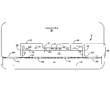
accordance with the present application. Figure 1 shows a cross-sectional view
of the structure
of the layers of a sensor 10. Sensor 10 includes a sensor chip 90 and a non-
conductive carrier
140. The sensor chip 90 includes a conductive substrate 130, a dielectric
layer 120, a sensing
layer 110, and an insulating layer 100. The non-conductive carrier 140 is a
chip carrier 140.
The circuitry used to obtain measurements from the sensor 10 is not shown in
Figure 1.
[0011] The non-conductive carrier 140 has a first surface 141 and an opposing
second surface
143. The conductive substrate 130 has a first surface 131, an opposing second
surface 132, and
side-walls 135. The sidewalls 135 are also referred to herein as "sidewall
surfaces 135". The
conductive substrate 130 overlays a portion 144 of the surface 141 of the non-
conductive carrier
140. The second surface 132 of the conductive substrate 130 contacts the
portion 144 of the
first surface 141 of the non-conductive carrier 140. The dielectric layer 120
overlays the
2
CA 02900509 2015-08-14
conductive substrate 130. The second surface 222 of the dielectric layer 120
contacts the first
surface 131 of the conductive substrate 130.
[0012] The dielectric layer 120 includes a gate dielectric 121 having a first
thickness t1 and a
field dielectric 122 having a second thickness t2. The field dielectric 122
has a first surface 221
and an opposing second surface 222. The gate dielectric 121 has a first
surface 223 and an
opposing second surface 222. As shown in Figure 1, the gate dielectric 121 and
the field
dielectric 122 are formed contiguously in the dielectric layer 120 and they
share the second
surface 222. Since the second thickness t2 is greater than the first thickness
ti, the gate
dielectric 121 is surrounded by the field dielectric 122.
[0013] The sensing layer 110 has first surface 111 and an opposing second
surface 112. The
sensing layer 110 overlays the first surface 223 of the gate dielectric 121.
The second surface
112 of the sensing layer 110 contacts the first surface 223 of the gate
dielectric 121.
[0014] The insulating layer 100 conformally coats at least the side-walls 135
of the conductive
substrate 130. The first surface 111 of the sensing layer 110 is uncoated by
the insulating layer
100. As shown in Figure 1, the insulating layer 100 conformally coats: 1) the
side-walls 135 of
the conductive substrate 130; 2) the first surface 221 of the field dielectric
122; and 3) an
exposed surface 142 of the non-conductive carrier 140. The exposed surface 142
of the non-
conductive carrier 140 is defined as that portion of the surface 141 of the
non-conductive carrier
140 that is not overlaid by the conductive substrate 130 of the sensor chip
90.
[0015] In one implementation of this embodiment, the conformal coatings are
formed by vapor
based chemical reactions, which are repeatedly cycled to deposit an atomic
layer with each
deposition cycle. The insulating layer 100 deposited in this manner is a high
quality dielectric
that contiguously and evenly deposits material on all exposed surfaces, even
vertical surfaces.
The insulating layer 100 is also referred to herein as "atomic-layer-
deposition layer 100", an
"ALD layer 100", and "ALD 100".
[0016] In one implementation of this embodiment, the insulating layer 100 is
deposited using
Atomic Layer Deposition (ALD). In another implementation of this embodiment,
the insulating
layer 100 is deposited using one of the types of chemical vapor deposition
(CVD). In yet
another implementation of this embodiment, the insulating layer 100 is
approximately or less
than 1000 Angstroms.
3
CA 02900509 2015-08-14
[0017] The first surface 111 of the sensing layer 110 is the surface that is
exposed to the
environment to be sensed. As shown in Figure 1, the first surface 111 of the
sensing layer 110
is the surface that is exposed to a conductive fluid 50.
[0018] In one implementation of this embodiment, the sensor 10 is a pH sensor
10 used to
measure the pH of a liquid (e.g., conductive fluid 50). The dielectric layer
120 and sensing
layer 110 are operable to sense pH when exposed to the conductive fluid 50.
When pH sensors
are used in high pressures situations (e.g., deep in the ocean) or in repeated
pressure cycling
situations, the pH sensors are known to cause bending of the non-conductive
carrier.
[0019] In prior art pH sensors that use an 0-ring to insulate the sidewalls
from the conductive
fluid, the bending of the non-conductive carrier under high pressure and/or
repeated pressure
cycling causes the 0-ring to pop off of the device so the sidewalls are
exposed. Similarly, in
prior art pH sensors that use epoxy to insulate the sidewalls from the
conductive fluid, the
bending of the non-conductive carrier under high pressure and/or repeated
pressure cycling
causes the epoxy to delaminate from the sides walls so the sidewalls are
exposed to the fluid
being sensed. In both cases, a desired current flows from the sidewall to the
sensing surface and
the prior art pH sensors have erroneous measurements.
[0020] Because the ALD layer 100 of the sensor 10 has high integrity and good
adhesion to the
sidewalls 135, the ALD layer 100 is able to withstand high pressure and
repeated pressure
cycling without cracking or shifting away from the sidewall 134. Even when the
non-
conductive carrier 140 bends under the pressure, the thin atomic layers of the
ALD layer 100 of
the sensor 10 remain adhered to the sidewalls 135. Thus, no undesired stray
currents are
generated to flow between the sidewalls 135 and the first surface 111 of the
sensing layer via
the conductive fluid 50 and the sensor 10 accurately measures the pH of the
conductive fluid 50.
[0021] In one implementation of this embodiment, the insulating layer 100
conformally coats
the side-walls 135 of the conductive substrate 130 but does not coat the
entire first surface 221
of the field dielectric 122. In another implementation of this embodiment, the
conductive
substrate 130 is a silicon substrate. In another implementation of this
embodiment, the
conductive substrate 130 is a p doped silicon substrate. In yet another
implementation of this
embodiment, the non-conductive carrier 140 is formed from a plastic material
as known to one
skilled in the art.
[0022] Figure 2 shows a layer structure of a sensor 11 with circuit components
195. Sensor 11
is similar to sensor 10 in that it includes a non-conductive carrier 140 and a
sensor chip 91. The
4
CA 02900509 2015-08-14
sensor chip 91 includes a conductive substrate 130, a dielectric layer 120
including the gate
dielectric 121 and the field dielectric 122, a sensing layer 110, and an
insulating layer 100 (ALD
100). The sensor 11 also includes a first electrode 145 inlaid in the non-
conductive carrier 140,
a second electrode 146 inlaid in the non-conductive carrier 140, a first via
170 in the conductive
substrate 130, and a second via 175 in the conductive substrate 130, and an
insulating layer 180.
The first via 170 and the second via 175 are electrically conductive.
[0023] A first conductive material 181 that extends through the insulating
layer 180 is formed
in the insulating layer 180. In one implementation of this embodiment, the
first conductive
material 181 is formed by etching a through hole in the insulating layer 180
and filling the
through hole with a metal or metal alloy. A second conductive material 182
that extends
through the insulating layer 180 is formed in the insulating layer 180. In one
implementation of
this embodiment, the second conductive material 182 is formed by etching a
second through
hole in the insulating layer 180 and filling the second through hole with a
metal or metal alloy.
The first and second conductive material 181 and 182 are also referred to
herein as respective
first and second conductive pads 181 and 182.
[0024] The first via 170 electrically connects a source diffusion region
represented generally at
150 to the first electrode 145 via the first conductive pad 181 in the
insulating layer 180. The
second via 175 electrically connects a drain diffusion region represented
generally at 160 to the
second electrode 146 via the second conductive pad 182 in the insulating layer
180. The circuit
components 195, when electrically connected to the first electrode 145 and the
second electrode
146 as shown in Figure 2, are operable to sense a current generated within the
sensor 11 based
on the environment of the sensing layer 110, e.g., the conductive fluid 50.
The circuit
components 195 are shown in Figure 2 to be external to the conductive fluid
50. However, in
embodiments, the circuit components 195 are packaged with the sensor 11 and
the package is in
the conductive fluid 50. In one implementation of this embodiment, there is no
insulating layer
180.
[0025] In one implementation of this embodiment, the insulating layer 180 is
formed from
silicon oxide. In this case, the insulating layer 180 is a silicon dioxide
layer 180. In another
implementation of this embodiment, the conductive substrate 130 is a silicon
substrate with
appropriate p-n junction layers to form the desired channel. In yet another
implementation of
this embodiment, the first via 170 is formed by etching a first cavity 171 in
the conductive
substrate 130 and coating the inner surface of the first cavity 171 with a
conductive material
172. In one implementation of this embodiment, the conductive material 172 is
a metal or metal
CA 02900509 2015-08-14
alloy (for example, gold). The conductive material 172 electrically contacts
the first conductive
pad 181 in the insulating layer 180. In yet another implementation of this
embodiment, the
second via 175 is formed by etching a second cavity 176 in the conductive
substrate 130 and
coating the inner surface of the second cavity 176 with a conductive material
177. In one
implementation of this embodiment, the conductive material 177 is a metal or
metal alloy (for
example, gold). The conductive material 177 electrically contacts the second
conductive pad
182 in the insulating layer 180.
[0026] The sensor 11 is operable as a pH sensor 11. The pH of a conductive
fluid 50 is a
function of the number of hydrogen ions in the conductive fluid 50 as is known
to one skilled in
the art. The material in the sensing layer 110 (e.g., gate 110) absorbs
hydrogen ions (protons)
from the conductive fluid 50. When hydrogen ions interact with the sensing
layer 110, the
sensor chip 91 in the sensor 11 is operable as a field effect transistor (FET)
91, in which the
sensing layer 110 functions as a gate 110 and the conductive substrate 130
functions as a
channel. As the gate 110 is charged up by the interacting hydrogen ions in the
conductive fluid
50, the current flow in the channel 130 increases. The current is measured
between the source
diffusion region 150 and the drain diffusion region 160.
[0027] As is understandable to one skilled in the art upon reading and
understanding this
document, the sensor 10 of Figure 1 can be implemented with the first
electrode 145, the second
electrode 146, the first via 170 in the conductive substrate 130, the second
via 175 in the
conductive substrate 130 and the insulating layer 180 as shown in Figure 2.
[0028] Figure 3 shows a layer structure of a sensor 12. The layer structure of
sensor 12 differs
from the sensor 11 of Figure 3 in that the ALD 100 does not cover the exposed
surface 142 of
the non-conductive carrier 140 that is not overlaid by the conductive
substrate 130. In this
embodiment, the ALD 100 is deposited on the sensor chip 90 formed by the
conductive
substrate 130, the dielectric layer 120, and the sensing layer 110 before the
sensor chip 90 is
placed on the non-conductive carrier 140. For the embodiment of the sensor 10
shown in
Figure 1, the sensor chip 90 is placed on the non-conductive carrier 140 and
then the ALD 100
is deposited on the sensor chip 90 and the non-conductive carrier 140.
[0029] As is understandable to one skilled in the art upon reading and
understanding this
document, the sensor 12 can be implemented with the first electrode 145, the
second electrode
146, the first via 170 in the conductive substrate 130, the second via 175 in
the conductive
substrate 130 and the insulating layer 180 as described above with reference
to Figure 2.
6
CA 02900509 2015-08-14
100301 Figure 4 is a flow diagram of a method 400 of fabricating sensors that
are immune to
stray currents in accordance with the present application. The method 400 is
described with
reference to the sensors 10, 11, and 12 of respective Figures 1, 2, and 3.
However, it is to be
understood, that method 400 is applicable to adaptations or variations of the
sensors shown and
described herein.
[0031] At block 402, a first surface 131 of a conductive substrate 130 is
coated with a dielectric
layer 120. The dielectric layer 120 can be deposited using one or more of a
variety of
techniques for deposition known to one skilled in the art. In one
implementation of this
embodiment, the dielectric layer 120 is deposited with a second thickness t2
and a portion of the
dielectric layer 120 is etched to form a gate dielectric 121 with a first
thickness ti in the field
dielectric 122. In this case, the first thickness t1 is less than the second
thickness t2. In another
implementation of this embodiment, a first via 170 and a second via 175 are
formed in the
conductive substrate 130 (Figure 2). In yet another implementation of this
embodiment, the
first via 170 is formed by etching a first cavity 171and coating the inner
surface of the first
cavity with a conductive material 172 while ensuring that the conductive
material 172 is
isolated from the conductive substrate 130 as is understandable to one skilled
in the art. In yet
another implementation of this embodiment, the second via 175 is formed by
etching a second
cavity 176 and coating the inner surface of the second cavity 176 with a
conductive material
177 while ensuring that the conductive material 177 is isolated from the
conductive substrate
130 as is understandable to one skilled in the art.
100321 At block 404, a portion (e.g., the gate dielectric 121) of the
dielectric layer 120 is coated
with a sensing layer 110. The sensing layer 110 can be deposited using one or
more of a variety
of techniques for deposition known to one skilled in the art. In one
implementation of this
embodiment, the sensing layer 110 is formed from metal oxides as known to one
skilled in the
art. The sensing layer 110 is deposited on the portion of the dielectric layer
120 that was etched
back to form the gate dielectric 121 with a first thickness ti. In one
implementation of this
embodiment, the first thickness ti of the gate dielectric 121 in combination
with the thickness of
the sensing layer 110 are less than the second thickness t2 of the field
dielectric 122. In this
case, the first surface 111 of the sensing layer 110 is closer to the first
surface 131 of the
conductive substrate 130 than the first surface 221 of the field dielectric
122.
[0033] At block 406, the conductive substrate 130 is segmented to form sensor
chips and
sidewalls 135 of the conductive substrate 130 are exposed due to the
segmenting. In one
implementation of this embodiment, the segmenting process is done by sawing
the substrate
7
CA 02900509 2015-08-14
(wafer) into a plurality of sensor chips 90. In another implementation of this
embodiment, the
segmenting process is done by notching the substrate and cleaving the
substrate to break along
the crystalline planes due to the notches.
[0034] At block 408, an insulating layer 100 is conformally formed over at
least the sidewalls
135 of the conductive substrate 130 that was exposed by the segmenting at
block 406. The first
surface 111 of the sensing layer 110 is uncoated by the insulating layer 100.
In this manner,
after die separation exposes the sidewalls 135 and after the sensor chip 90 or
91 is attached to a
header (e.g., non-conductive carrier 140), the conformal insulating layer 100
coats the entire
sensor 10, 11, or 12 to eliminate any conductive path through the conductive
fluid 50 between
the first surface 111 of the sensing layer 110 and the sidewalls 135.
[0035] The insulating layer 100 is conformally formed in vapor based chemical
reaction used to
deposit a dielectric onto the exposed sidewall surfaces of the conductive
substrate 130. In
particular, Atomic Layer Deposition (ALD) and other forms of chemical vapor
deposition
(CVD) are able to deposit a high quality dielectric on all exposed surfaces,
even vertical
surfaces. Because the ALD has high integrity and good adhesion, it withstands
high pressure
and pressure cycling. A processing step is needed to make clear the first
surface 111 of the
sensing layer 110 of the ALD.
[0036] Often the sensing material of the sensing layer 110 is fragile and can
be damaged when
the ALD 100 is removed from the first surface 111 of the sensing layer 110.
This damage can
be prevented by depositing and patterning a sacrificial layer on the sensing
layer 110 before the
ALD 100 is deposited to protect the material of the sensing layer 110. The
sacrificial layer is
removed later. For example, the first surface 111 of the sensing layer 110 is
protected from the
insulating layer by a deposition of a protective sacrificial material (e.g.,
aluminum) on the first
surface 111 of the sensing layer 110 prior to the deposition of the conformal
insulating layer
100 on the sidewalls 135 of the conductive substrate. Then the protective
material (e.g.,
aluminum) protecting the first surface 111 of the sensing layer 110 and the
insulating layer 100
conformally formed over the protective material is lifted off of the first
surface 111 of the
sensing layer 110 so the first surface 111 of the sensing layer 110 is exposed
to the
environment.
[0037] In one implementation of this embodiment, the conductive substrate 130
of the sensor
chip 90 or 91 is positioned on a non-conductive carrier 140 prior to step 408
so that the non-
8
CA 02900509 2015-08-14
conductive carrier 140 is also conformally coated with the insulating layer
100. This
embodiment is shown in the sensor 10 of Figure 1.
[0038] In another implementation of this embodiment, the conductive substrate
130 of the
sensor chip 90 or 91 is positioned on a non-conductive carrier 140 after step
408 so that the non-
conductive carrier 140 is not conformally coated with the insulating layer
100. This
embodiment is shown in the sensor 12 of Figure 3.
[0039] In yet another implementation of this embodiment, a first electrode 145
and a second
electrode 146 are formed in the non-conductive carrier 140 along with any
required trace lines
to communicatively couple the first electrode 145 and the second electrode 146
to circuit
components 195 (Figure 2). In this case, an insulating layer 180 is formed
between the non-
conductive carrier 140 and the second surface 132 of the conductive substrate
130. This ensures
the first electrode 145 and the second electrode 146 are electrically isolated
from the conductive
substrate 130 except for the points of contact between the first via 170 and
the first electrode
145 and between the second via 175 and the second electrode 146 when the
sensor chip 90 or 91
is positioned on the non-conductive carrier 140. In one embodiment, the
insulating layer 180 is
a layer of silicon dioxide 180 formed between the non-conductive carrier 140
and a second
surface 132 of the conductive substrate 130. In another implementation of this
embodiment, the
insulating layer 180 is an oxide layer.
Example embodiments
[0040] Example 1 includes a sensor comprising: a conductive substrate having
side-walls; a
dielectric layer overlaying a first surface of the conductive substrate, the
dielectric layer
including a gate dielectric having a first thickness and a field dielectric
having a second
thickness; a sensing layer overlaying a first surface of the gate dielectric;
a non-conductive
carrier wherein a second surface of the conductive substrate overlays a
portion of the non-
conductive carrier; and an insulating layer conformally coating at least the
side-walls of the
conductive substrate, wherein a first surface of the sensing layer is uncoated
by the insulating
layer.
[0041] Example 2 includes the sensor of Example 1, wherein the insulating
layer is an atomic
layer having a thickness less than 1000 Angstroms.
[0042] Example 3 includes the sensor of any of Examples 1-2, wherein the
insulating layer
conformally coats the field dielectric.
9
CA 02900509 2015-08-14
[0043] Example 4 includes the sensor of any of Examples 1-3, wherein the
insulating layer
conformally coats the field dielectric, and an exposed surface of the non-
conductive carrier.
[0044] Example 5 includes the sensor of any of Examples 1-4, further
comprising: circuit
components, wherein the dielectric layer, the sensing layer, and the circuit
components are
operable to sense pH of a conductive fluid when the sensing layer is exposed
to the conductive
fluid.
[0045] Example 6 includes the sensor of any of Examples 1-5, further
comprising: a first
electrode; a second electrode; a first via formed in the conductive substrate,
the first via
electrically connecting a source diffusion region to the first electrode; and
a second via formed
in the conductive substrate, the second via electrically connecting a drain
diffusion region to the
second electrode, wherein, when the sensor is operable, the sensing layer
functions as a gate,
and the conductive substrate functions as a channel.
[0046] Example 7 includes the sensor of Example 6, further comprising: a layer
of silicon
dioxide formed between the non-conductive carrier and the second surface of
the conductive
substrate, the layer of silicon dioxide overlaying the first electrode and the
second electrode.
[0047] Example 8 includes the sensor of any of Examples 1-7, wherein the
conductive substrate
is a silicon substrate.
[0048] Example 9 includes the sensor of any of Examples 1-8, wherein the
conductive substrate
is a p doped silicon substrate.
[0049] Example 10 includes the sensor of any of Examples 1-9, wherein the
dielectric layer and
sensing layer sense pH when exposed to a conductive fluid.
[0050] Example 11 includes a method of forming a sensor that is immune to
stray currents,
comprising coating a first surface of a conductive substrate with a dielectric
layer; coating a
portion of the dielectric layer with a sensing layer; segmenting the
conductive substrate,
wherein sidewalls are exposed; and conformally forming an insulating layer
over at least the
sidewalls, wherein a first surface of the sensing layer is uncoated by the
insulating layer.
[0051] Example 12 includes the method of Example 11, further comprising:
positioning the
conductive substrate on a non-conductive carrier.
[0052] Example 13 includes the method of any of Examples 11-12, further
comprising:
positioning the conductive substrate on a non-conductive carrier prior to
conformally forming
CA 02900509 2015-08-14
the insulating layer over at least the sidewalls, wherein the insulating layer
overlays a portion of
a surface of the non-conductive carrier.
[0053] Example 14 includes the method of any of Examples 11-13, further
comprising; etching
a portion of the dielectric layer, wherein coating the portion of the
dielectric layer with the
sensing layer includes: coating the etched portion of the dielectric layer
with the sensing layer.
[0054] Example 15 includes the method of any of Examples 11-14, further
comprising: forming
a first electrode in a non-conductive carrier; forming a second electrode in
the non-conductive
carrier; forming a first via in the conductive substrate; forming a second via
in the conductive
substrate; and positioning the conductive substrate on a non-conductive
carrier.
[0055] Example 16 includes the method of Example 15, further comprising:
forming an
insulating layer between the non-conductive carrier and a second surface of
the conductive
substrate, the insulating layer overlaying the first electrode and the second
electrode; forming a
first conductive material in the insulating layer; and forming a second
conductive material in the
insulating layer.
[0056] Example 17 includes the method of any of Examples 15-16, further
comprising: forming
a layer of silicon dioxide between the non-conductive carrier and a second
surface of the
conductive substrate, the layer of silicon dioxide overlaying the first
electrode and the second
electrode; forming a first conductive pad in the layer of silicon dioxide; and
forming a second
conductive pad in the layer of silicon dioxide.
[0057] Example 18 includes the method of any of Examples 15-17, wherein
forming the first
via in the conductive substrate comprises: etching a first cavity in the
conductive substrate; and
coating an inner surface of the first cavity with a metal or a metal alloy,
and wherein forming
the first via in the conductive substrate comprises: etching a second cavity
in the conductive
substrate; and coating an inner surface of the second cavity with the metal or
the metal alloy.
[0058] Example 19 includes a pH sensor comprising: a non-conductive carrier; a
first electrode
inlaid in the non-conductive carrier; a second electrode inlaid in the non-
conductive carrier; a
conductive substrate having a first surface, a second surface, and side-walls,
the conductive
substrate overlaying at least a portion of the non-conductive carrier; a
dielectric layer overlaying
the first surface of the conductive substrate, the dielectric layer including
a gate dielectric
having a first thickness and a field dielectric having a second thickness; a
sensing layer
overlaying a first surface of the gate dielectric; an insulating layer
conformally coating at least
the side-walls of the conductive substrate, wherein a first surface of the
sensing layer is
11
CA 02900509 2015-08-14
uncoated by the insulating layer; a first via formed in the conductive
substrate, the first via
electrically connecting a source diffusion to the first electrode; and a
second via formed in the
conductive substrate, the second via electrically connecting a drain diffusion
to the second
electrode, wherein, when the pH sensor is operable, the sensing layer
functions as a gate, and
the conductive substrate functions a channel.
[0059] Example 20 includes the pH sensor of Example 19, further comprising: a
layer of oxide
formed between the non-conductive carrier and the second surface of the
conductive substrate
overlaying the first electrode and the second electrode; a first conductive
pad extending through
the layer of oxide; and a second conductive pad extending through the layer of
oxide.
100601 Although specific embodiments have been illustrated and described
herein, it will be
appreciated by those of ordinary skill in the art that any arrangement, which
is calculated to
achieve the same purpose, may be substituted for the specific embodiment
shown. This
application is intended to cover any adaptations or variations of the present
invention.
Therefore, it is manifestly intended that this invention be limited only by
the claims and the
equivalents thereof.
12