Note: Descriptions are shown in the official language in which they were submitted.
CA 02903362 2015-09-01
DESCRIPTION
POWER CONVERSION DEVICE
TECHNICAL FIELD
[0001] The present invention relates to a power
conversion device which rapidly disconnects a defective
power conversion unit among a plurality of power conversion
units provided in parallel with each other from a DC power
supply unit supplying DC power to each of the power
conversion units to continue to operate the other faultless
power conversion unit.
BACKGROUND ART
[0002] As a power source device which drives a large AC
load such as a motor or drives a plurality of AC loads in
parallel by using a DC power source as a power source, a
power conversion device where a plurality of power
conversion units are provided in parallel with each other
is used. Fig. 3 is a schematic configurational diagram
illustrating such a type of the power conversion device,
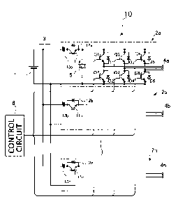
and the reference numeral 1 denotes a DC power supply unit.
The DC power supply unit 1 is configured with, for example,
a diode circuit of rectifying and smoothing a commercial AC
power source, a battery, or the like.
[0003] In addition, the reference numeral 2 (2a to 2n)
denotes a plurality of power conversion units which are
connected to the DC power supply unit 1 through a DC link
1
CA 02903362 2015-09-01
portion 3 to be provided in parallel with each other. Each
of the power conversion units 2 (2a to 2n) is configured
with an inverter unit which converts the DC power supplied
from the DC power supply unit 1 to AC power and outputs the
AC power. For example, output terminals 4 (4a to 4n) of
the power conversion units 2 (2a to 2n) are connected in
parallel to be used as power output terminals for a large
AC load. Alternatively, a plurality of AC loads are
individually connected to the output terminals 4 (4a to 4n)
of the plurality of the power conversion units 2 (2a to 2n).
[0004] Fig. 3 illustrates an example of a configuration
of the power conversion unit 2a. Each of the power
conversion units 2 (2a to 2n) is provided with three sets
of half-bridge circuits which are configured, for example,
by connecting six semiconductor switching elements Q1 to Q6
consisting of IGBTs or the like in such a manner that every
two semiconductor switching elements are connected in
series and inserted between a positive electrode and a
negative electrode of the DC input terminal in parallel
with each other. Each of the semiconductor switching
elements Q1 to Q6 is driven to be alternatively turned on
and off with a predetermined phase difference for each
half-bridge circuit to switch a DC voltage applied to the
half-bridge circuit. In addition, each of the power
conversion units 2 (2a to 2n) is configured to connect
2
CA 02903362 2015-09-01
serial connection points which are central points of the
half-bridge circuits to the output terminals 4 (4a to 4n)
so as to output a three-phase AC power having a
predetermined voltage.
[0005] In addition, the reference letters D1 to D6
denote freewheeling diodes which are connected in reverse
parallel with the respective semiconductor switching
elements Q1 to Q6. In addition, the reference numeral 5
denotes a condenser which is arranged between each DC input
terminals of each of the power conversion units 2 (2a to
2n) to stabilize the DC voltage applied to the power
conversion unit 2 (2a to 2n). In addition, the reference
numeral 6 denotes a control circuit which controls the
semiconductor switching elements Q1 to Q6 to be turned on
and off as described above. The power conversion device
having such a configuration is described in detail, for
example, in Patent Document 1 or the like.
[0006] In Patent Document 1 described above, switches 7
using mechanical contacts are provided as circuit breakers
in the DC input portions of the plurality of the power
conversion units 2 (2a to 2n). Furthermore, Patent
Document 1 discloses a configuration where DC reactors 8
are installed in the DC link portion 3 with respect to the
DC power supply unit 1. When defect such as short-circuit
occurs in any one of the power conversion units 2 (2a to
3
CA 02903362 2015-09-01
2n), the switch 7 disconnects the defective power
conversion unit 2 (2a to 2n) from the DC power supply unit
1. By doing so, only the remaining faultless power
conversion units 2 (2a to 2n) can be operated.
[0007] However, until the defective power conversion
unit 2 (2a to 2n) is disconnected by the switch 7, an
excessive current flows from the other faultless power
conversion units 2 (2a to 2n) to the short-circuit point of
the defective power conversion unit 2 (2a to 2n). Due to
the excessive current flow, the other faultless power
conversion units 2 (2a to 2n) may be fallen into an
excessive current state. The DC reactors 8 have a function
of preventing the faultless power conversion units 2 (2a to
2n) from being fallen into the excessive current state by
restricting the rise of the current flowing in the other
faultless power conversion units 2 (2a to 2n) at the time
of occurrence of the short-circuit fault.
CITATION LIST
PATENT DOCUMENT
[0008] Patent Document 1: JP4726624B2
SUMMARY OF THE INVENTION
PROBLEM TO BE SOLVED BY THE INVENTION
[0009] However, in a case where the DC reactors 8 are
inserted in the DC link portions 3, the response
characteristics of the power conversion units 2 (2a to 2n)
4
are deteriorated. In other words, the responsiveness to
the change of the input DC voltage at the normal operation
time of the power conversion units 2 (2a to 2n) is
deteriorated. Moreover, an operation response delay of the
switch 7 is typically in the order of milli-seconds, and
thus, the responsiveness to the short-circuit fault is not
so high.
[0010] The invention has been made in consideration of
such circumstances, and an object thereof is to provide a
power conversion device having a simple configuration and
high responsiveness by rapidly disconnecting a defective
power conversion unit among a plurality of the power
conversion units which are provided in parallel with each
other from a DC power supply unit so that the other
faultless power conversion units can continue to be
operated.
MEANS FOR SOLVING PROBLEM
Date Recue/Date Received 2020-07-14
[0011] According to an aspect of the present invention,
there is provided a power conversion device comprising:
a DC power supply unit;
a plurality of power conversion units which are
provided in parallel with each other through a DC link
portion to convert DC power supplied from the DC power supply
unit to AC power and output the AC power;
a plurality of semiconductor switch elements each
interposed between a corresponding one of the plurality of
power conversion units and the DC power supply unit, each of
the plurality of semiconductor switch elements being provided
in a forward direction with respect to a flowing direction of
a current inherent to the DC power supply from the DC power
supply unit to each of the plurality of power conversion
units to individually restrict or block the DC power supplied
to the each of the plurality of power conversion units; and
a control circuit which monitors an occurrence of a
short-circuit current occurring in each of the plurality of
power conversion units and controls a semiconductor switch
element, of the plurality of semiconductor switch elements,
connected to a corresponding power conversion unit, of the
plurality of power conversion units, where the short-circuit
current occurs, to be turned off to stop the DC power supply
to the short-circuited power conversion unit and to
electrically disconnect the short-circuited power conversion
5a
Date Recue/Date Received 2020-07-14
unit from the DC link portion so as to maintain operations of
other remaining power conversion units, of the plurality of
power conversion units, where no short-circuit occurs,
wherein the control circuit detects the short-circuit
current of the power conversion unit based on a decrease in a
voltage of a smoothing capacitor installed between the DC
link portion and the short-circuited power conversion unit
caused by a short-circuited semiconductor switching element
constituting a main body of the power conversion unit or an
increase in a current flowing into the short-circuited power
conversion unit from the DC link portion in accordance with
the voltage decrease, and turns off the semiconductor switch
element corresponding to the short-circuited power conversion
unit.
5b
Date Recue/Date Received 2020-07-14
In addition, the control circuit may be configured to
[0012]
control the semiconductor switching element to be turned
off by detecting, for example, the following current: a
current supplied from the DC power supply unit to the power
conversion unit, a current flowing in the semiconductor
switching element constituting a main body of the power
conversion unit, or a short-circuit current caused by
short-circuit fault of the power conversion unit due to a
decrease in a DC voltage applied to the semiconductor
switch element.
[0013] In addition, the DC power supply unit may be
contigured with, for example, a voltage-control-type PWM
converter whicn generates a predetermined DC voltage by
using semiconductor switching elements such as IGBIs or
MOS-FETs. Further, each of the power conversion unitsmaY be
6
Date Recue/Date Received 2020-07-14
configured with, for example, an inverter unit which
generates a three-phase AC power. Furthermore, the
semiconductor switch element may be configured with, for
example, an IG3T with which a diode is in reverse parallel
or a reverse conducting IGBT which allows a current to flow
bidirectionally. In addition, the semiconductor switch
element may be inserted in at least one of a positive electrode
side and a negative electrode side of a DC input portion of
each of the power conversion units.
EFFECT OF THE INVENTION
[0014] According to the power conversion device having
the above-described configuration, element characteristics
of the semiconductor switch elements interposed between
the power conversion units and the DC power supply unit can
be effectively utilized to restrict a power, particularly,
a current supplied to each of the power conversion units.
Therefore, it is possible to effectively prevent an
excessive current from unintentionally flowing in the
semiconductor switching elements constituting each of the
power conversion units.
[0015] In addition, in a case where short-circuit fault
occurs in the power conversion unit, the semiconductor
switch element connected to the power conversion unit
where the fault occurs is controlled to be turned off under
the control of the control circuit, so that the power
7
Date Recue/Date Received 2020-07-14
conversion unit can be rapidly disconnected from the DC
power supply unit. Furthermore, since the response delay
of the semiconductor switch element is typically in the
order of micro-seconds, in comparison with the case of the
related art where a general switch using a mechanical
contact is used as a circuit breaker, the power conversion
unit where the fault occurs can be disconnected from the DC
power supply unit at a sufficiently high speed.
[0016] Therefore, according to the power conversion
device according to the invention, unlike the device of the
related art where the DC reactors are provided to the DC
input portion of the power conversion units, the problem of
the operation response delay does not occur in the power
conversion units in the normal state. In addition, since
there is no need for a DC reactor, its inductance value
needs not to be adjusted, and the operation responsiveness
of each power conversion unit can be sufficiently fast.
[0017] In addition, at the time of detection of the
short-circuit current in the power conversion unit, only by
controlling the semiconductor switch element to be
turned off, the power conversion unit where the short-
circuit fault occurs can be rapidly disconnected from the
DC power supply unit. Therefore, the other faultless power
conversion unit can continue to be operated stably without
causing the above-described problem of an excessive current.
8
Date Recue/Date Received 2020-07-14
Accordingly, by using the semiconductor switch elements
having a current restriction function and a DC link circuit
disconnection function, the whole configuration of the
power conversion device can be simplified while securing
the operation characteristics, and thus, it is possible to
obtain excellent practical effects in terms that the
faultless power conversion units can continue to be
operation.
BRIEF DESCRIPTION OF DRAWINGS
[001E] Fig. 1 is a schematic configurational diagram
illustrating main components of a power conversion device
according to an embodiment of the invention;
Fig. 2 is a schematic configurational diagram
illustrating main components of a power conversion device
according to another embodiment of the invention; and
Fig. 3 is a schematic configurational diagram
illustrating main components of a power conversion device
of the related art.
DESCRIPTION OF PREFERRED EMBODIMENTS
[0019] Hereinafter, power conversion devices according
to embodiments of the invention will be described with
reference to the drawings.
[0020] Fig. 1 is a diagram illustrating a schematic
configuration of main components of a power conversion
device 10 according to an embodiment of the invention. The
9
Date Recue/Date Received 2020-07-14
same components as those of the power conversion device of
the related art illustrated in Fig. 3 are denoted by the
same reference numerals. In addition, redundant
description of the components denoted by the same reference
numerals is omitted. Further, in the embodiment, the DC
power supply unit 1 can be realized, for example, as a
voltage-control type PWM converts or the like which
switches a DC input voltage by using semiconductor
switching elements such as IGBTs or MOS-FETs to generate a
predetermined DC output voltage.
[0021] As a feature of the power conversion device 10
according to the embodiment, semiconductor switch
elements 11 (11a to 11n) configured with, for example,
IGBTs are installed as circuit breakers in series with
respective DC input portions of the plurality of the power
conversion units 2 (2a to 2n) which are arranged in
parallel with each other. Diodes 12 (12a to 12n) are
connected in reverse parallel with the respective
semiconductor switch elements 11 (11a to 11n). The
diodes 12 (12a to 12n) have a function of flowing an AC
cross current component superposed on the DC power caused
by a delay of a switching operation of the above-described
switching elements Q1 to QS, variations of the components
of the power conversion units 2 (2a to 2n) or the like.
[0022] Herein, the example where each of the
Date Recue/Date Received 2020-07-14
semiconductor switch elements 11 (11a to 11n) is
inserted in series with a positive electrode side of the DC
input portion of the respective power conversion unit 2 (2a
to 2n) is illustrated. However, each of the semiconductor
switch elements 11 (11a to 11n) may be inserted in
series with a negative electrode side of the DC input
portion of the respective power conversion unit 2 (2a to
2n). In addition, as the semiconductor switch elements
11 (11a to 11n), reverse conducting IGBTs allowing current
to flow bidirectionally may be used.
[0023] In addition, in a case where the power conversion
units 2 (2a to 2n) have no abnormality, that is, in a case
where the power conversion units 2 (2a to 2n) operate
normally, the semiconductor switch elements 11 (11a to
11n) are controlled to be turned on under the control of
the control circuit 6. Therefore, the DC power supplied
from the DC power supply unit 1 through the DC link portion
3 is applied to each of the power conversion units 2 (2a to
2n) through the respective semiconductor switch
elements
11 (11a to 11n).
[0024] The maximum current of the DC current which flows
into the power conversion units 2 (2a to 2n) through the
turned-on semiconductor switch elements
11 (11a to 11n)
is restricted according to the element characteristics of
the respective semiconductor switch elements
11 (11a to
11
Date Recue/Date Received 2020-07-14
11n). Therefore, the DC power applied to the respective
half-bridge circuit constituting the main body of each of
the power conversion units 2 (2a to 2n) is restricted.
Therefore, if a defect such as a short-circuit does not
occur in the semiconductor switching elements Q1 to Q6
constituting the half-bridge circuits, an excessive current
does not flow in each of the half-bridge circuits.
[0025] However, when a defect such as a short-circuit
occurs in the semiconductor switching elements Q1 to Q6, a
terminal voltage of the condenser 5 installed to the DC
input portion of the power conversion unit 2 (2a to 2n),
that is, a so-called DC link voltage is decreased.
According to the decrease in the terminal voltage, a short-
circuit current of which current value is abnormally large
flows from the DC power supply unit 1 to the power
conversion unit 2 (2a to 2n). The control circuit 6
monitors the occurrence of the short-circuit current
through, for example, current detectors 13 (13a to 13n)
provided to the DC input portions.
[0026] When the short-circuit current is detected, the
control circuit 6 controls the semiconductor switch
elements 11 (11a to 11n) in the power conversion unit 2 (2a
to 2n) where the short-circuit current is detected to be
turned off. Therefore, the control circuit 6 blocks the DC
power which is to be supplied from the DC power supply unit
12
Date Recue/Date Received 2020-07-14
1 to the power conversion unit 2 (2a to 2n). Due to the
control of the semiconductor switch elements
11 (11a to
11n) to be turned off, the power conversion unit 2 (2a to
2n) where the short-circuit fault occurs is disconnected
from the DC power supply unit 1. The disconnection of the
power conversion unit 2 (2a to 2n) from the DC power supply
unit 1 depends on element characteristics of the
semiconductor switch elements 11 (11a to 11n), and the
disconnection is rapidly performed, for example, only with
a response delay which is in the order of micro-seconds.
[0027] Therefore, before the aforementioned abnormal
current flows in the other faultless power conversion units
2 (2a to 2n) caused by the short-circuit fault, the power
conversion unit 2 (2a to 2n) where the short-circuit fault
occurs is disconnected. Accordingly, the excessive current
caused by the short-circuit fault does not flow in the
other faultless power conversion units 2 (2a to 2n). In
addition, if the excessive current caused by the short-
circuit fault is to flow in the other faultless power
conversion units 2 (2a to 2n), the current restriction is
performed by the above-described semiconductor switch
elements 11 (11a to 11n). By doing so, the occurrence of
the excessive current in the faultless power conversion
units 2 (2a to 2n) is prevented in advance. Accordingly,
the power conversion unit 2 (2a to 2n) where the short-
13
Date Recue/Date Received 2020-07-14
circuit fault occurs is disconnected, and the other
remaining faultless power conversion units 2 (2a to 2n) can
continue to be stably operated.
[0028] In particular, according to the power conversion
device 10 having the above-described configuration, the DC
current (DC power) which is to flow in the power conversion
units 2 (2a to 2n) can be restricted by using the
semiconductor switch elements 11 (11a to 11n). At the
same time, the power conversion device 10 having the above-
described configuration can rapidly disconnect the power
conversion unit 2 (2a to 2n) where the short-circuit fault
occurs from the DC power supply unit 1 by using the
semiconductor switch elements 11 (lia to iln) at the
time of detection of the short-circuit current. Therefore,
it is possible to obtain excellent effects in terms that
the configuration is simple and the operation response
characteristics of the power conversion units 2 (2a to 2n)
in normal operation is not sacrificed.
[0029] In a case where the main body of each of the
power conversion units 2 (2a to 2n) is configured with, for
example, a three-level inverter as illustrated in Fig. 2,
the following configuration is preferred. In addition to
the configuration where each semiconductor switch
element 11 (11a to 11n) is provided in series to the
positive electrode side of each DC input portion of each of
14
Date Recue/Date Received 2020-07-14
the power conversion units 2 (2a to 2n), each semiconductor
switch element
14 (14a to 14n) is provided in series to
the negative electrode side of each DC input portion.
Herein, the three-level inverter is also referred to as a
neutral point clamp inverter.
[00301 Namely, schematically, the three-level inverter
inputs a central point voltage obtained by dividing the DC
output voltage of the DC power supply unit 1 by two, the
aforementioned positive-electrode voltage, and the
aforementioned negative-electrode voltage and switches the
DC voltage among these voltages. The output voltages
obtained by switching among these voltages are synthesized
to generate AC power, which is closer to a sinusoidal wave
than that by the inverter illustrated in Fig. 1. The
three-level inverter is described in detail in, for example,
JP2011-193646A.
[0031] In Fig.
2, the reference numeral 15 (15a to 15n)
denotes diodes which are connected in reverse parallel with
the respective semiconductor switch elements
14 (14a to
14n). In addition, the reference numeral 16 (16a to 16n)
denotes current detectors which detect current flowing in
the respective semiconductor switch elements
14 (14a to
14n). In addition, the reference numerals 17a, 17b, and
17c denote bidirectional switches for controlling
potentials of serial connection points of the respective
Date Recue/Date Received 2020-07-14
half-bridge circuits in the three-level inverter.
[0032] In Fig. 2, the DC power supply unit 1 is
equivalently illustrated as DC power sources la and lb
outputting 1/2 of the DC voltage so that the DC power
supply unit outputs the central point voltage which is to
be applied to the three-level inverter. In addition, two
condensers 5a and 5b which are interposed between the
positive-electrode voltage point and the central voltage
point and between the central voltage point and the
negative-electrode voltage point, respectively, are used in
the three-level inverter.
[0033] Therefore, in a case where each of the power
conversion units 2 (2a to 2n) is configured by using the
three-level inverter as the main body, as illustrated in
Fig. 2, the semiconductor switch elements 11 (11a to
11n) and 14 (14a to 14n) are provided at the positive
electrode side and the negative electrode side in each of
the DC input portions of the power conversion units 2 (2a
to 2n), respectively. Therefore, according to the short-
circuit fault at the upper arm side or the lower arm side
of each half-bridge circuit, the semiconductor switch
elements 11 (11a to 11n) of the positive electrode side or
the semiconductor switch
elements 14 (14a to 14n) of the
negative electrode side are controlled to be turned off.
Accordingly, the power conversion unit 2 (2a to 2n) may be
16
Date Recue/Date Received 2020-07-14
disconnected from the respective DC power sources la and lb
of the DC power supply unit 1.
[0034] In this case, at the same time when the power
conversion unit 2 (2a to 2n) where the short-circuit fault
occurs is disconnected from one of the DC power sources la
and lb of the DC power supply unit 1, under the control of
the control circuit 6, the power conversion unit 2 (2a to
2n) is preferably disconnected from the other one of the DC
power sources la and lb. By doing so, the power conversion
unit 2 (2a to 2n) where the short-circuit fault occurs can
be completely disconnected from the DC power supply unit 1.
In addition, similarly to the above-described embodiment,
the other faultless power conversion units 2 (2a to 2n) can
continue to be stably operated.
[0035] The invention is not limited to the above-
described embodiments. For example, although depending on
a power amount of the power conversion units 2 (2a to 2n),
mOS-FDTs or bipolar transistors may be used as the
semiconductor switch elements 11 (11a to 11n) and 14
(14a to 14n). Furthermore, switching elements using SiC
(silicon carbide) elements may be employed. In addition,
in the embodiments, the short-circuit current is detected
from the current flowing in the power conversion unit 2 (2a
to 2n) by the current detectors 13 (13a to 13n) and 16 (16a
to 16n) installed in the DC input portions of the power
17
Date Recue/Date Received 2020-07-14
conversion units 2 (2a to 2n).
[0036] However, in the case of using the IGBTs having
current sense terminals as the semiconductor switching
elements Q1 to Q6, the occurrence of the short-circuit
current can be monitored by directly detecting the current
flowing from the current sense terminal into the
semiconductor switching elements Q1 to Q6. Alternatively,
the short-circuit of the semiconductor switching elements
Ql to Q6 may be detected based on the DC voltages applied
to the semiconductor switching elements Q1 to Q6, for
example, collector voltages of the IGHTs.
[0037] In addition, as well as the power conversion
units 2 (2a to 2n) generating a three-phase AC power, the
invention can be applied to power conversion units 2 (2a to
2n) generating a single-phase AC power or other power
conversion devices where the power conversion circuits are
provided in parallel with each other. In addition, in the
embodiments, in the control circuit 6, the short-circuit of
the power conversion units 2 (2a to 2n) is detected, and
the semiconductor switch.
elements 11 (11a to 11n) and 14
(14a to 14n) are controlled to be turned on and off.
However, the function of controlling the semiconductor
switch elements 11 (11a to 11n) and 14 (14a to 14n) to
be turned on and off according to the detection of the
short-circuit may be provided to each of the power
18
Date Recue/Date Received 2020-07-14
conversion units 2 (2a to 2n). The invention can be
embodied in various modifications without departing from
the spirit of the invention.
EXPLANATIONS OF LETTERS OR NUMERALS
[0038] 1: DC power supply unit
la, lb: DC power source
2 (2a to 2n): power conversion unit
3: DC link portion
5, 5a, 5b: condenser
6: control circuit
10: power conversion device
11 (11a to 11n): semiconductor switch element
12 (12a to 12n): diode
13 (13a to 13n): current detector
14 (14a to 14n): semiconductor switch element
15 (15a to 15n): diode
16 (16a to 16n): current detector
17a, 17b, 17c: bidirectional switch
Ql to Q6: semiconductor switching element
D1 to D6: freewheeling diode
19
Date Recue/Date Received 2020-07-14