Note: Descriptions are shown in the official language in which they were submitted.
TITLE OF THE INVENTION
Coating for a Titanium Alloy Substrate
BACKGROUND OF THE INVENTION
[0001] Due to its unique combination of hardness, wear resistance, low
deposition temperature
(below 150 C), biocompatibility, and friction characteristics (friction
coefficient below 0.1), DLC
is ideally suited for applications in a variety of fields, including
tribology, corrosion protection, and
medical devices. However, in applications of DLC as hard coatings, the high
residual stresses
associated with its deposition gives rise to poor adhesion strength, brittle
fracture and delamination
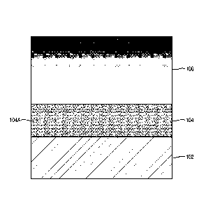
under high local loading. Referring to Figure 1A, for example, there is shown
a secondary electron
microscopy ("SEM") image of a cross section of ungraded DLC coating 106
deposited on a
Titanium-Aluminum-Niobium (Ti6A17Nb) substrate 102. As shown in Figure 1, the
ungraded DLC
coating 106 exhibited poor tolerance for deformations underneath it ("eggshell
effect"), and due to
its brittleness and low elongation at failure developed cracks 108. Layer 107
is a platinum coating
used to enhance conductivity around the ungraded DLC coating 106 deposited on
a Titanium-
.. Aluminum-Niobium (Ti6A17Nb) substrate 102. Figure 1B illustrates a contrast
adjusted SEM
image shown in Figure 1A, which better shows the cracks in the DLC coating.
The cracks 108
compromise the integrity of the DLC coating 106 and lead to failure of the DLC
coated Ti6A17Nb
substrate 102 (e.g., delaminated prosthesis) by generating hard wear debris.
Accordingly, a need
exists for more robust coated metal-based prostheses that are able exhibit
high tolerance for both
.. elastic and plastic deformations, and therefore prevent development of
cracks that compromise the
integrity of the coating and the coated prostheses.
BRIEF SUMMARY OF THE INVENTION
100021 In one aspect, the present invention provides for a surgical
implant. In one embodiment,
the surgical implant comprises a metallic substrate. In one embodiment, there
is a tantalum
.. interlayer disposed adjacent to the metallic substrate. In one embodiment,
the tantalum interlayer
comprises a-tantalum and amorphous tantalum. In one embodiment, the surgical
implant includes at
least one DLC layer disposed adjacent the tantalum interlayer. In one
embodiment, the tantalum
interlayer has a phase gradient between the metallic substrate side and the
DLC side. In one
embodiment, the tantalum interlayer has a phase gradient from I3-tantalum to a-
tantalum between the
metallic substrate side and the DLC side. In one embodiment, the amorphous
tantalum of the
CAN_DMS: \134243876\1 1
Date Recue/Date Received 2020-07-03
tantalum interlayer has a crystallinity gradient increasing from the metallic
substrate side to the DLC
side. In one embodiment, the DLC layer has a hardness value and an elastic
modulus value. In one
embodiment, the hardness value of the DLC layer has a gradient increasing away
from the tantalum
side. In one embodiment, the elastic modulus value of the DLC layer has a
gradient increasing away
from the tantalum side.
[0003] In some embodiments, the metallic substrate of the surgical
implant independently
includes titanium, a titanium based alloy, a cobalt based alloy or steel. In
some embodiments, the
tantalum interlayer of the surgical implant has a thickness ranging from 1 nm
to 2 p.m.
[0004] In some embodiments, the tantalum interlayer independently
further comprises an
element or compound, wherein the element or compound promotes the growth of a-
tantalum. In
some such embodiments, the element independently includes titanium, niobium,
tungsten and
combinations thereof. In other such embodiments, the compound independently
includes titanium
compound, niobium compound, tungsten compound or combinations thereof.
[0005] In some embodiments, the tantalum interlayer of the surgical
implant further comprises
tantalum compound nanoparticles. In some embodiments, the tantalum interlayer
of the surgical
implant is a nanocomposite of tantalum-carbide and tantalum. In some
embodiments, the surgical
implant has a DLC layer with a hardness value gradient that increases from 12
GPa to 22 GPa. In
some embodiments, the surgical implant has a DLC layer with an elastic modulus
value gradient that
increases from 120 GPa to 220 GPa. In some embodiments, the surgical implant
has at least one
DLC layer comprising a plurality of alternating sub-layers. In one embodiment,
the plurality of
alternating sub-layers comprises a DLC sub-layer and a doped DLC sub-layer. In
one embodiment,
the doped DLC sub-layer is doped with a metal. In one embodiment, the metal
doped DLC sub-
layer is doped with titanium.
[0006] In another aspect, the present invention provides for a method
for manufacturing an
exemplary surgical implant in accordance with present invention. In one
embodiment, the method
comprises inserting a metallic substrate into a vacuum system. In one
embodiment, the method
includes cleaning the metallic substrate by Ar+ bombardment at a RF self bias
ranging from about -
200 volts to about -2000 volts. In one embodiment, the metallic substrate is
cleaned by Ar+
bombardment at a RF self bias of -600 volts.
[0007] In one embodiment, the method includes depositing a tantalum
interlayer while applying
an electrical bias to the substrate. In one embodiment, the bias is a RF self
bias. In one embodiment,
the applied RF self bias ranges from -50 volts to -600 volts. In one
embodiment, the applied RF self
2
Date Recue/Date Received 2020-07-03
bias is changed in predetermined increments. In one embodiment, the applied RF
self bias is
changed in stepwise increment ranging from a 5 volt step to a 50 volt step.
[0008] In one embodiment, the method includes depositing a DLC layer. In
one embodiment,
the DLC layer is deposited by introducing a hydrocarbon at a second specified
RF self bias to the
substrate. In one embodiment, the DLC layer is deposited by introducing a
hydrocarbon at the
second RF self bias that is changed from -50 volts to ¨ 600 volts in a
stepwise increment. In one
embodiment, the applied second RF self bias is changed in stepwise increment
ranging from a 5 volt
step to a 50 volt step. In one embodiment, the DLC layer is deposited by
introducing a hydrocarbon
having a molecular weight ranging from 92 g/mole to 120 g/mole. In one
embodiment, the DLC
layer is deposited by introducing a hydrocarbon independently selected from
the group consisting of
toluene, xylene, trimethyl benzene, and combinations thereof
[0009] In some embodiments, the method for manufacturing a surgical
implant according to the
present invention includes the step of introducing an acetylene atmosphere at
a third RF self bias to
the substrate. In one embodiment, the applied third RF self bias is changed
from -50 volts to ¨ 600
volts in a second stepwise increment. In one embodiment, the second stepwise
increment ranges
from a 5 volt step to a 50 volt step.
[0010] In another embodiment, a method for manufacturing a surgical
implant, in accordance
with the present invention, includes the steps of: (a) inserting a metallic
substrate into a vacuum
system; (b) cleaning the metallic substrate by Ar+ bombardment at a RF self
bias to the substrate
ranging from about -200 volts to about -2000 volts, preferably at a RF self
bias of -600 volts; (c)
depositing a tantalum interlayer by applying an electrical bias, including a
RF self bias, to the
substrate during tantalum deposition, said RF self bias ranging from -50 volts
to -600 volts; (d)
depositing a DLC layer by introducing an acetylene atmosphere at a RF self
bias, wherein the RF
self bias is changed from -50 volts to ¨ 600 volts in a stepwise increment for
a first time period; (e)
.. after the first time period, introducing a organotitanium source into the
acetylene atmosphere for a
second time period; and (f) repeating steps (d) and (e) up to one hundred
repetitions. In one
embodiment, the stepwise increment ranges from a 5 volt step to a 50 volt
step.
BRIEF DESCRIPTION OF THE SEVERAL VIEWS OF THE DRAWINGS
[0011] The foregoing summary, as well as the following detailed
description of embodiments of
the surgical implant and method of manufacturing the same, will be better
understood when read in
conjunction with the appended drawings of an exemplary embodiment. It should
be understood,
however, that the invention is not limited to the precise arrangements and
instrumentalities shown.
3
Date Recue/Date Received 2020-07-03
[0012] In the drawings:
[0013] Figure 1A is a scanning electron microscopy (SEM) image of a non-
graded tantalum and
DLC lubricant coating deposited on TiAl6Nb7;
[0014] Figure 1B is a scanning electron microscopy (SEM) image of a non-
graded tantalum and
DLC lubricant coating deposited on TiAl6Nb7;
[0015] Figure 2 is a schematic cross-section view of a coated surgical
implant in accordance
with an exemplary embodiment of the present invention;
[0016] Figure 3 is a schematic cross-section view of a graded DLC
lubricant coating deposited
on a surgical implant in accordance with an exemplary embodiment of the
present invention;
[0017] Figure 4 is a schematic cross-section view of a surgical implant
having a coating
comprising alternating DLC and metal-doped DLC layers.
[0018] Figure 5 is a schematic cross-section view of a surgical implant
in accordance with an
exemplary embodiment of the present invention having the tantalum interlayer
comprising
nanocomposite tantalum carbide and tantalum dispersed in tantalum.
[0019] Figure 6A is an image showing a top perspective view of a cervical
disc prosthesis DLC
coated in accordance with an exemplary embodiment of the present invention.
[0020] Figure 6B is another image showing a top perspective view of a
cervical disc prosthesis
shown in Figure 6A.
DETAILED DESCRIPTION OF THE INVENTION
[0021] Referring to the drawings in detail, wherein like reference numerals
indicate like
elements throughout, there is shown in Figures 2-6 a schematic cross-section
view of a coated
surgical implant, in accordance with exemplary embodiments of the present
invention.
[0022] The present invention generally relates to prosthetic orthopedic
implants, particularly to
joint components such as for use with knees, hips, shoulders, elbows, toes,
fingers, wrists, ankles
and spinal disc replacements. More specifically, the present invention relates
to a method of making
a non-modular prosthetic joint component having a metal substrate, tantalum
interlayer, and DLC
layer.
[0023] In an aspect, the present invention provides a surgical implant
having a metallic substrate
coated with at least one layer comprising DLC. As shown in Figure 2, in one
embodiment, surgical
implant comprises a metallic substrate 102 have a coating that includes a
tantalum interlayer 104
disposed adjacent to metallic substrate 102. In one embodiment, surgical
implant includes metallic
substrate 102 and tantalum interlayer 104 comprising a-tantalum. In one
embodiment, surgical
4
Date Recue/Date Received 2020-07-03
implant includes metallic substrate 102 and tantalum interlayer 104 comprising
amorphous
tantalum. In one embodiment, surgical implant includes metallic substrate 102
and tantalum
interlayer 104 comprising a-tantalum and amorphous tantalum. In one
embodiment, surgical
implant includes metallic substrate 102 and at least one DLC layer 106
disposed adjacent tantalum
interlayer 104. In one embodiment, the tantalum interlayer has a phase
gradient between the
metallic substrate side and the DLC side. In one embodiment, surgical implant
includes metallic
substrate 102 and tantalum interlayer 104 comprising an amorphous tantalum
having a crystallinity
gradient. In one embodiment, surgical implant includes metallic substrate 102
and tantalum
interlayer 104 comprising an amorphous tantalum having a crystallinity
gradient that increases from
metallic substrate 102 side to DLC layer 106 side. In one embodiment, surgical
implant includes
tantalum interlayer 104 having a phase gradient from I3-tantalum to oc-
tantalum.
100241 In one embodiment, surgical implant includes metallic substrate
102, tantalum interlayer
104 and DLC layer 106 having a hardness value and an elastic modulus value. In
one embodiment,
surgical implant includes metallic substrate 102, tantalum interlayer 104 and
DLC layer 106 having
a hardness value and an elastic modulus value, wherein the hardness value has
a gradient increasing
away from tantalum interlayer 104 side. In one embodiment, surgical implant
includes metallic
substrate 102, tantalum interlayer 104 and DLC layer 106 having a hardness
value and an elastic
modulus value, wherein the elastic modulus value has a gradient increasing
away from the tantalum
interlayer 104 side.
100251 In one embodiment, surgical implant includes metallic substrate 102;
tantalum interlayer
104 disposed adjacent to metallic substrate 102 and comprising a-tantalum and
amorphous tantalum;
at least one DLC layer 106 disposed adjacent tantalum interlayer 104. In one
embodiment, surgical
implant includes metallic substrate 102; tantalum interlayer 104 disposed
adjacent to metallic
substrate 102 and comprising a-tantalum and amorphous tantalum; and at least
one DLC layer 106
disposed adjacent tantalum interlayer 104, wherein the amorphous tantalum has
a concentration
gradient increasing from metallic substrate 102 side to the DLC layer 106
side. In one embodiment,
surgical implant includes metallic substrate 102; tantalum interlayer 104
disposed adjacent to
metallic substrate 102 and comprising a-tantalum and amorphous tantalum; and
at least one DLC
layer 106 disposed adjacent tantalum interlayer 104, wherein DLC layer 106 has
a hardness value
and an elastic modulus value; and wherein the hardness value has a gradient
increasing away from
tantalum interlayer 104 side. In one embodiment, surgical implant includes
metallic substrate 102;
tantalum interlayer 104 disposed adjacent to metallic substrate 102 and
comprising a-tantalum and
5
Date Recue/Date Received 2020-07-03
amorphous tantalum; and at least one DLC layer 106 disposed adjacent tantalum
interlayer 104,
wherein the elastic modulus value has a gradient increasing away from tantalum
interlayer 104 side.
100261 Metallic substrate 102 of surgical implant in accordance with
exemplary embodiments of
the present invention can comprise any suitable metal, metal alloy or a
combination of both.
Generally, metallic substrate 102 can include any metals and metal alloys that
possess any
advantageous combinations of properties, thermal and mechanical
characteristics, including little
heating and high levels of endurance strength during alternating repetition of
loads. In one
embodiment, metallic substrate 102 comprises a titanium-based alloy. In one
embodiment, metallic
substrate 102 comprises a titanium-based alloy selected from the group
consisting of TiAl6V4,
TiA16Nb7 and a combination thereof In one embodiment, metallic substrate 102
comprises a
cobalt-chromium (CoCrMo) alloy. In one embodiment, metallic substrate 102
comprises steel. In
one embodiment, metallic substrate 102 comprises at least one element selected
from the group
consisting of titanium, nickel, iron, cobalt, niobium, zinc, tungsten,
molybdenum, and tantalum. In
one embodiment, metallic substrate 102 comprises a metal alloy in which at
least one of the
elements is selected from the group consisting of titanium, nickel, iron,
cobalt, niobium, zinc,
tungsten, molybdenum, and tantalum. In one embodiment, metallic substrate 102
comprises
titanium and/or a titanium alloy selected from the group consisting of
unalloyed commercially pure
(CP) titanium, TiAl6V4, TiAl6Nb7, or nickel-titanium (superelastic NiTi or
shape-memory NiTi).
100271 In some exemplary embodiments, metallic substrate 102 of surgical
implant 100 in
accordance with the present invention preferably comprises a titanium alloy.
Benefits of using
titanium alloys as prosthesis materials include high mechanical load-bearing
capacity, high fatigue
strength, elasticity, high chemical stability, improved magnetic resonance
imaging ("MM") and
computed tomography ("CT") compatibility, and superior biocompatibility. Also,
many different
types of surgical implants, including bone plates, pins, artificial knee and
hip joints, and
intervertebral disk prostheses can be advantageously fabricated from titanium-
based alloys.
However, titanium based alloys exhibit inadequate wear behavior in
articulation in addition to
difficult finishing capabilities, requiring a wear-resistant coating.
100281 Referring to Figures 2 and 3, tantalum interlayer 104 in
accordance with an exemplary
embodiment of the present invention is preferably disposed adjacent to
metallic substrate 102. In
one embodiment, tantalum interlayer 104 comprises crystalline tantalum. In one
embodiment,
tantalum interlayer 104 comprises crystalline tantalum and amorphous tantalum.
In one
embodiment, tantalum interlayer 104 comprises a-tantalum. In one embodiment,
tantalum interlayer
104 comprises I3-tantalum and a-tantalum. In one embodiment, tantalum
interlayer 104 comprises
6
Date Recue/Date Received 2020-07-03
I3-tantalum and amorphous tantalum. In one embodiment, tantalum interlayer 104
comprisesI3-
tantalum, a-tantalum and amorphous tantalum.
[0029] Referring to Figure 3, in one embodiment, tantalum interlayer 104
comprises
nanocomposite tantalum with a tantalum compound, such as a carbide, as a
sublayer 104B. In one
embodiment, sublayer 104B comprises an element or compound to promote a-
tantalum growth. In
one such embodiment, the element independently includes titanium, niobium or
tungsten. In
another such embodiment, the compound independently includes titanium
compound, niobium
compound or tungsten compound. In one embodiment, tantalum interlayer 104
comprises tantalum
as a sublayer 104A and nanocomposite tantalum and a tantalum compound, for
example, tantalum
carbide, as a sublayer 104. As shown in Figure 5, in one embodiment, tantalum
interlayer 104 is
entirely comprised of nanocomposite tantalum and a tantalum compound (see 104C
in Figure 5). In
one embodiment, tantalum interlayer 104 comprises a nanocomposite of a-
tantalum and a tantalum
compound. In one embodiment, tantalum interlayer 104 comprises at least one
tantalum layer, of 13-
tantalum, a-tantalum and mixtures thereof, and at least one nanocomposite
tantalum and tantalum
compound layer.
[0030] Referring to Figures 3 and 5, in one embodiment, tantalum
interlayer 104 comprises
tantalum compound nanoparticles, such as tantalum carbide. In one embodiment,
tantalum
interlayer 104 comprises tantalum compound nanoparticles and tantalum, as I3-
tantalum, a-tantalum
and mixtures thereof. In one embodiment, tantalum interlayer 104 comprises I3-
tantalum,
.. amorphous tantalum and tantalum compound nanoparticles. In one embodiment,
tantalum interlayer
104 comprises a-tantalum, amorphous tantalum and tantalum compound
nanoparticles. In one
embodiment, tantalum interlayer 104 comprises I3-tantalum, amorphous tantalum
and tantalum
compound nanoparticles dispersed in tantalum interlayer 104. In one
embodiment, tantalum
interlayer 104 comprises a-tantalum, amorphous tantalum and tantalum compound
nanoparticles
dispersed in tantalum interlayer 104. In one embodiment, tantalum interlayer
104 comprises f3-
tantalum, a-tantalum, amorphous tantalum and tantalum compound nanoparticles
dispersed in
tantalum interlayer 104.
100311 Referring to Figures 2-5, in one embodiment, tantalum interlayer
104 comprises from
about 50 to about 100 atomic percent (or at.%) a-tantalum. In one embodiment,
tantalum interlayer
104 comprises from about 50 to about 100 atomic percent (or at.%) amorphous
tantalum. In one
embodiment, tantalum interlayer 104 comprises from about 70 to about 99 atomic
percent (or at.%)
tantalum compound nanoparticles. In one embodiment, tantalum interlayer 104
comprises from
about 10 to about 30 atomic percent (or at.%) a-tantalum; from about 10 to
about 30 atomic percent
7
Date Recue/Date Received 2020-07-03
(or at.%) amorphous tantalum; and from about 50 to about 99 atomic percent (or
at.%) tantalum
compound nanoparticles.
[0032] In some embodiments, tantalum interlayer 104 comprises
nanocomposite tantalum
including a tantalum-carbide composition. In one embodiment, tantalum
interlayer 104 comprises
nanocomposite tantalum having from about 5 to about 50 atomic percent (or
at.%) tantalum and
from about 50 to about 99 atomic percent (or at.%) of tantalum carbide.
[0033] Referring to Figures 2-5, in some embodiments, tantalum
interlayer 104 comprises a
phase gradient extending at least partially there through. In one embodiment,
tantalum interlayer
104 comprises a tantalum phase gradient. In one embodiment, tantalum
interlayer 104 comprises a
phase gradient including a-tantalum. In one embodiment, tantalum interlayer
104 comprises a phase
gradient including amorphous tantalum. In some embodiments, tantalum
interlayer 104 comprises a
phase gradient including a-tantalum, wherein the phase gradient extends from
metallic substrate 102
side of surgical implant to DLC layer 106 side of surgical implant. In some
embodiments, tantalum
interlayer 104 comprises a phase gradient including amorphous tantalum,
wherein the phase gradient
extends from metallic substrate 102 side of surgical implant to DLC layer 106
side of surgical
implant. In some embodiments, tantalum interlayer 104 comprises a
crystallinity gradient extending
at least partially there through. In one embodiment, tantalum interlayer 104
comprises a tantalum
crystallinity gradient. In one embodiment, tantalum interlayer 104 comprises a
crystallinity gradient
including a-tantalum. In one embodiment, tantalum interlayer 104 comprises a
crystallinity gradient
from I3-tantalum to a-tantalum. In some embodiments, tantalum interlayer 104
comprises a
crystallinity gradient including a-tantalum, wherein the crystallinity
gradient extends from metallic
substrate 102 side of surgical implant to DLC layer 106 side of surgical
implant.
[0034] Referring to Figures 2-5, in some embodiments, tantalum
interlayer 104 has a thickness
ranging from about 1 nm to about 2 p.m (or 2000 nm). In one embodiment,
tantalum interlayer 104
has a thickness having a value in a range selected from the group consisting
of: from about 1 nm to
about 10 nm, from about 1 nm to about 20 nm; from about 1 nm to about 40 nm,
from about 1 nm to
about 60 nm; from about 1 nm to about 100 nm; from about 10 nm to about 100
nm, from about 10
nm to about 300 nm, from about 10 nm to about 500 nm, from about 10 nm to
about 700 nm, from
about 10 nm to about 1000 nm, from about 10 nm to about 1200 nm, from about 10
nm to about
1400 nm, from about 10 nm to about 1600 nm, from about 10 nm to about 1800 nm,
from about 10
nm to about 2000 nm; from about 20 nm to about 100 nm, from about 20 nm to
about 300 nm, from
about 20 nm to about 500 nm, from about 20 nm to about 700 nm, from about 20
nm to about 1000
nm, from about 20 nm to about 1200 nm, from about 20 nm to about 1400 nm, from
about 20 nm to
8
Date Recue/Date Received 2020-07-03
about 1600 nm, from about 20 nm to about 1800 nm, from about 20 nm to about
2000 nm; from
about 50 nm to about 100 nm, from about 50 nm to about 300 nm, from about 50
nm to about 500
nm, from about 50 nm to about 700 nm, from about 50 nm to about 1000 nm, from
about 50 nm to
about 1200 nm, from about 50 nm to about 1400 nm, from about 50 nm to about
1600 nm, from
about 50 nm to about 1800 nm, from about 50 nm to about 2000 nm; from about
100 nm to about
200 nm, from about 100 nm to about 300 nm, from about 100 nm to about 400 nm,
from about 100
nm to about 500 nm, from about 100 nm to about 600 nm, from about 100 nm to
about 700 nm,
from about 100 nm to about 800 nm, from about 100 nm to about 900 nm, from
about 100 nm to
about 1000 nm, from about 100 nm to about 1100 nm, from about 100 nm to about
1200 nm, from
about 100 nm to about 1300 nm, from about 100 nm to about 1400 nm, from about
100 nm to about
1500 nm, from about 100 nm to about 1600 nm, from about 100 nm to about 1700
nm, from about
100 nm to about 1800 nm, from about 100 nm to about 1900 nm, from about 200 nm
to about 300
nm, from about 300 nm to about 400 nm, from about 400 nm to about 500 nm, from
about 500 nm
to about 600 nm, from about 200 nm to about 400 nm, from about 300 nm to about
500 nm, from
about 400 nm to about 600 nm, from about 500 nm to about 700 nm, from about
200 nm to about
500 nm, from about 300 nm to about 600 nm, from about 400 nm to about 700 nm,
from about 500
nm to about 800 nm, from about 200 nm to about 600 nm, from about 300 nm to
about 700 nm,
from about 400 nm to about 800 nm, from about 500 nm to about 900 nm, from
about 200 nm to
about 700 nm, from about 300 nm to about 800 nm, from about 400 nm to about
900 nm, from about
500 nm to about 1000 nm, from about 200 nm to about 800 nm, from about 300 nm
to about 900
nm, from about 400 nm to about 1000 nm, from about 500 nm to about 1100 nm,
from about 200
nm to about 900 nm, from about 300 nm to about 1000 nm, from about 400 nm to
about 1100 nm,
from about 500 nm to about 1200 nm, from about 200 nm to about 1000 nm, from
about 300 nm to
about 1100 nm, from about 400 nm to about 1200 nm, from about 500 nm to about
1300 nm, from
about 200 nm to about 1100 nm, from about 300 nm to about 1200 nm, from about
400 nm to about
1300 nm, from about 500 nm to about 1400 nm, from about 200 nm to about 1200
nm, from about
300 nm to about 1300 nm, from about 400 nm to about 1400 nm, from about 500 nm
to about 1500
nm, from about 200 nm to about 1300 nm, from about 300 nm to about 1400 nm,
from about 400
nm to about 1500 nm, from about 500 nm to about 1600 nm, from about 200 nm to
about 1400 nm,
from about 300 nm to about 1500 nm, from about 400 nm to about 1600 nm, from
about 500 nm to
about 1700 nm, from about 200 nm to about 1500 nm, from about 300 nm to about
1600 nm, from
about 400 nm to about 1700 nm, from about 500 nm to about 1800 nm, from about
200 nm to about
1600 nm, from about 300 nm to about 1700 nm, from about 400 nm to about 1800
nm, from about
9
Date Recue/Date Received 2020-07-03
500 nm to about 1900 nm, from about 200 nm to about 1700 nm, from about 300 nm
to about 1800
nm, from about 400 nm to about 1900 nm, from about 500 nm to about 2000 nm,
from about 200
nm to about 1800 nm, from about 300 nm to about 1900 nm, from about 400 nm to
about 2000 nm,
from about 200 nm to about 1900 nm, from about 300 nm to about 2000 nm, from
about 200 nm to
.. about 2000 nm, from about 600 nm to about 700 nm, from about 600 nm to
about 800 nm, from
about 700 nm to about 800 nm, from about 600 nm to about 900 nm, from about
700 nm to about
900 nm, from about 800 nm to about 900 nm, from about 600 nm to about 1000 nm,
from about
700 nm to about 1000 nm, from about 800 nm to about 1000 nm, from about 900 nm
to about 1000
nm, from about 1000 nm to about 1100 nm, from about 1100 nm to about 1200 nm,
from about 600
nm to about 1100 nm, from about 700 nm to about 1100 nm, from about 800 nm to
about 1100 nm,
from about 900 nm to about 1100 nm, from about 1000 nm to about 1200 nm, from
about 1100 nm
to about 1300 nm, from about 600 nm to about 1200 nm, from about 700 nm to
about 1200 nm,
from about 800 nm to about 1200 nm, from about 900 nm to about 1200 nm, from
about 1000 nm to
about 1300 nm, from about 1100 nm to about 1400 nm, from about 600 nm to about
1300 nm, from
about 700 nm to about 1300 nm, from about 800 nm to about 1300 nm, from about
900 nm to about
1300 nm, from about 1000 nm to about 1400 nm, from about 1100 nm to about 1500
nm, from
about 600 nm to about 1400 nm, from about 700 nm to about 1400 nm, from about
800 nm to about
1400 nm, from about 900 nm to about 1400 nm, from about 1000 nm to about 1500
nm, from about
1100 nm to about 1600 nm, from about 600 nm to about 1500 nm, from about 700
nm to about 1500
nm, from about 800 nm to about 1500 nm, from about 900 nm to about 1500 nm,
from about 1000
nm to about 1600 nm, from about 1100 nm to about 1700 nm, from about 600 nm to
about 1600 nm,
from about 700 nm to about 1600 nm, from about 800 nm to about 1600 nm, from
about 900 nm to
about 1600 nm, from about 1000 nm to about 1700 nm, from about 1100 nm to
about 1800 nm,
from about 600 nm to about 1700 nm, from about 700 nm to about 1700 nm, from
about 800 nm to
about 1700 nm, from about 900 nm to about 1700 nm, from about 1000 nm to about
1800 nm, from
about 1100 nm to about 1900 nm, from about 600 nm to about 1800 nm, from about
700 nm to
about 1800 nm, from about 800 nm to about 1800 nm, from about 900 nm to about
1800 nm, from
about 1000 nm to about 1900 nm, from about 1100 nm to about 2000 nm, from
about 600 nm to
about 1900 nm, from about 700 nm to about 1900 nm, from about 800 nm to about
1900 nm, from
about 900 nm to about 1900 nm, from about 1000 nm to about 2000 nm, from about
nm to about
nm, from about 600 nm to about 2000 nm, from about 700 nm to about 2000 nm,
from about 800
nm to about 2000 nm, and from about 900 nm to about 2000 nm.
Date Recue/Date Received 2020-07-03
[0035] Elemental carbon exists in a number of different forms called
allotropes. The most
common carbon allotrope is graphite (a-graphite). Diamond is a second
allotrope of carbon but is
much less common than graphite. Most graphite is a-graphite and it possesses a
layer structure in
which each carbon atom is directly bound to three other carbon atoms. The
bonding between the
carbon atoms in each layer structure is described as being three-fold
coordinated with trigonal planar
coordination geometry reflecting sp2hybridization of atomic orbitals. In
contrast, diamond
possesses a structure in which each carbon four-fold coordinated with
tetrahedral symmetry
reflecting sp3 hybridization of atomic orbitals. DLC is amorphous carbon with
high fraction of
diamond-like (sp3) bonds between carbon atoms. Reportedly DLC films comprise a
combination of
four-fold coordinated sp3 sites, as in diamond, and three-fold coordinated sp2
sites, as in graphite.
100361 Referring to Figures 2-5, in one embodiment, surgical implant
includes at least one DLC
layer 106 disposed adjacent tantalum interlayer 104. In one embodiment, DLC
layer 106 can be
synthesized by any suitable techniques including reactive magnetron
sputtering, by physical vapor
deposition ("PVD"), chemical vapor deposition ("CVD"), plasma chemical vapor
deposition
("PCVD"), plasma-enhanced chemical vapor deposition (PECVD), filtered cathodic
vacuum arc,
laser ablation, plasma beam source, and dense plasma focusing (DPF). In one
embodiment,
different deposition methods are used to fabricate DLC layer 106 with
preferred tribiological
properties. In one embodiment, DLC layer 106 comprises amorphous carbon or
amorphous
diamond (i-C, tetrahedral amorphous carbon ta-C). In one embodiment, DLC layer
106 comprises
hydrogenated amorphous carbon (a-C:H). In one embodiment, DLC layer 106
further including a
material comprising an element other than carbon. In one embodiment, DLC layer
106 further
including a material comprising an element selected from the group consisting
of silicon (Si),
nitrogen (N), a metal (Me), fluorine (F). Typically, a DLC film doped with Si,
N, metal atoms, and
F would be notated as a-Si-C:H, a-C:H-N, a-Me-C:H and a-C:H-F, respectively.
[0037] In some embodiments, DLC layer 106 has a hardness value and an
elastic modulus value.
Referring to Figures 2, 3, and 5, in one embodiment, DLC layer 106 has a
hardness value having a
gradient extending at least partially through DLC layer 106. In one
embodiment, DLC layer 106 has
a hardness value having a gradient increasing away from tantalum interlayer
104 side. In one
embodiment, DLC layer 106 has an elastic modulus value having a gradient
increasing away from
tantalum interlayer 104 side. In one embodiment, DLC layer 106 has hardness
value gradient that
increases from about 12 GPa to about 22 GPa. In one embodiment, DLC layer 106
has an elastic
modulus value gradient that increases: from about 120 GPa to about 220 GPa;
from about 100 GPa
to about 200 GPa; from about 50 GPa to about 100 GPa.
11
Date Recue/Date Received 2020-07-03
[0038] Referring to Figure 4, in some embodiments, at least one DLC
layer 106 comprises a
plurality of alternating sub-layers comprising a DLC sub-layer 106A and a
metal doped DLC sub-
layer 106B. In one embodiment, DLC layer 106 comprises a plurality of
alternating sub-layers
comprising a DLC sub-layer 106A and metal doped DLC sub-layer 106B, wherein
metal doped
DLC sub-layer 106B is doped with titanium. In one embodiment, at least one DLC
layer 106 has
graded hardness across at least a portion of it. In one embodiment, the at
least one DLC layer 106
has graded hardness tantalum from interlayer 104 side (see 106C in Figure 4).
[0039] Any specific examples of surgical implants described herein
should not be construed as
limiting the scope of the surgical implants of the present invention, but
rather as an exemplification
of preferred embodiments thereof Surgical implants that that are contemplated
herein include
prosthetics which are designed to replace damaged or missing body parts. In
some embodiments,
surgical implant is placed permanently or is removed from the patient's body
once it is no longer
needed. In some embodiments, surgical implant is selected from the group
consisting of hip
implants, chemotherapy ports and screws. In one embodiment, surgical implant
is an articulating
bone prosthesis. In one embodiment, surgical implant is selected from the
group consisting of a
total hip joint prosthesis and a total knee joint prosthesis. In one
embodiment, surgical implant is
metal-on-metal type joint prosthesis.
[0040] Surgical implant advantageously minimizes wear debris and
toxicity of wear products in
articulated joint prostheses, including metal-on-metal ("MOM") joint
prostheses, in which both of
the articulating surfaces are metal. The DLC and tantalum interlayer coatings
of surgical implant
beneficially improve performance of metal-on-metal ("MOM") joint prostheses by
providing coated
articulating surfaces that are hard (wear resistant), chemically inert
(biologically compatible) and
have low coefficients of friction. One such coating substance is DLC. The DLC
and tantalum
interlayer coatings of surgical implant beneficially improve chemical and
mechanical wear
resistance of the coated articulating implants. The DLC and tantalum
interlayer coatings of surgical
implant beneficially improve adhesion between the coatings and metallic
substrate 102 of surgical
implant to prevent or retard delamination of the coatings from metallic
substrate 102.
Compositional gradients of DLC layer 106 and/or tantalum interlayer 104
beneficially improve
adhesion between DLC layer 106 and/or tantalum interlayer 104 and metallic
substrate 102 and
minimize or prevent stresses would have otherwise developed in the non-graded
DLC layer 106
and/or non-graded tantalum interlayer 104 either due to lattice mismatch
(intrinsic stresses) or
difference in the thermal coefficients of non-graded DLC layer 106 and/or non-
graded tantalum
interlayer 104 and metallic substrate 102 (thermal stresses). Intrinsic
stresses and thermal stresses in
12
Date Recue/Date Received 2020-07-03
combination with stresses arising during articulation are known to cause
delamination of coated
surgical implants.
[0041] In another aspect, the present invention provides a method for
manufacturing surgical
implants in accordance with the exemplary embodiments of the present
invention. In one exemplary
embodiment, the method for manufacturing surgical implant comprises: (a)
inserting metallic
substrate 102 into a vacuum system; (b) cleaning metallic substrate 102; (c)
depositing tantalum
interlayer 104 onto metallic substrate 102; and (d) depositing DLC layer 106
onto tantalum
interlayer 104.
[0042] In one embodiment, the cleaning of metallic substrate 102 is
performed by ion
bombardment of metallic substrate 102 from a gaseous plasma. In one embodiment
of the ion
bombardment, ion bombardment energy and ion flux (density) are preferably
controlled by a radio
frequency (RF) power. However, in other embodiments, any other power sources
with which a
varying or static (DC) electric field can be established can be used. In one
embodiment, the ion
bombardment is preferably performed in vacuum so that a stable RF plasma can
be generated. In
one embodiment, RF power is used to control the gaseous plasma and ion
bombardment process. In
one embodiment, increasing the RF power, increases gaseous plasma potential
and direct current
(DC) equivalent bias. In one embodiment, increasing the RF power, increases
ion density of the
gaseous plasma. In one embodiment, decreasing the RF power decreases gaseous
plasma potential
and DC bias (ion bombardment energy). In one embodiment, decreasing the RF
power, decreases
ion density of the gaseous plasma. In one embodiment, the working pressure of
the gases in the
vacuum chamber in which metallic substrate 102 is inserted is used to control
the gaseous plasma
and ion bombardment process.
[0043] In one embodiment, cleaning of metallic substrate 102 comprises
applying argon ion
(Art) bombardment to metallic substrate 102 in vacuum. In one embodiment, Art
bombardment of
metallic substrate 102 in vacuum is performed at a RF self bias of -600 volts.
In one embodiment,
Art bombardment of metallic substrate 102 in vacuum is performed at a RF self
bias of ranging
from about -100 volts to about -2000 volts. In one such embodiment, the RF
self bias is changed in
stepwise increments ranging from a 5 volt step to a 50 volt step.
[0044] In one embodiment, the deposition of tantalum interlayer 104 on
metallic substrate 102
comprises applying an electrical bias to the substrate during tantalum
deposition from a tantalum
source. In one embodiment, the electrical bias is a RF self bias. In one
embodiment, the deposition
of tantalum interlayer 104 on metallic substrate 102 comprises applying a RF
self bias to the
substrate during a tantalum magnetron sputtering discharge, wherein the RF
self bias ranges from -
13
Date Recue/Date Received 2020-07-03
50 volts to -2000 volts, preferably -100 volts to -400 volts. In one
embodiment, deposition of
tantalum interlayer 104 on metallic substrate 102 comprises applying a RF self
bias to a substrate
during a tantalum magnetron sputtering discharge, wherein the RF self bias is
changed in a in a
stepwise manner. In one embodiment, deposition of tantalum interlayer 104 on
metallic substrate
102 comprises applying a RF self bias to a substrate during a tantalum
magnetron sputtering
discharge, wherein the RF self bias is changed in predetermined increments. In
one such
embodiment, the predetermined increments range from a 5 volt step to a 50 volt
step. In one
embodiment, deposition of tantalum interlayer 104 on metallic substrate 102
comprises applying a
RF self bias to a substrate during a tantalum magnetron sputtering discharge,
wherein the RF self
bias is changed in a stepwise manner and in predetermined increments. In one
such embodiment,
the predetermined increments range from a 5 volt step to a 50 volt step. In
one embodiment,
deposition of tantalum interlayer 104 on metallic substrate 102 comprises
applying a RF self bias to
a substrate during a tantalum magnetron sputtering discharge, wherein the RF
self bias is changed in
increments ranging from a 5 volt step to a 50 volt step.
[0045] In one embodiment, the deposition of DLC layer 106 comprises
introducing a
hydrocarbon having a molecular weight ranging from 92 g/mole to 120 g/mole, at
a second RF self
bias. In one embodiment, the deposition of DLC layer 106 comprises introducing
the hydrocarbon
having the molecular weight ranging from 92 g/mole to 120 g/mole, at the
second RF self bias,
wherein the second RF self bias is changed from -50 volts to ¨ 600 volts in a
stepwise increment. In
one embodiment, the deposition of DLC layer 106 comprises introducing the
hydrocarbon having
the molecular weight ranging from 92 g/mole to 120 g/mole, at the second RF
self bias, wherein the
second RF self bias is changed from -50 volts to ¨ 600 volts in a stepwise
increment, and wherein
the stepwise increment ranges from a 5 volt step to a 50 volt step. In one
embodiment, the
deposition of DLC layer 106 comprises introducing the hydrocarbon having the
molecular weight
ranging from 92 g/mole to 120 g/mole, at the second RF self bias, wherein the
hydrocarbon is
independently selected from the group consisting of: toluene, xylene,
trimethyl benzene, and
combinations thereof.
[0046] In one embodiment, the method for manufacturing surgical implants
in accordance with
the present invention further comprises the step of introducing an acetylene
atmosphere at a third RF
self bias. In one embodiment, the third RF self bias is changed from -50 volts
to ¨ 600 volts in a
second stepwise increment. In one embodiment, the second stepwise increment
ranges from a 5 volt
step to a 50 volt step.
14
Date Recue/Date Received 2020-07-03
[0047] In another embodiment, the method for manufacturing surgical
implants in accordance
with the present invention comprises the following: (a) inserting metallic
substrate 102 into a
vacuum system; (b) cleaning metallic substrate 102 by Ar+ bombardment at a
predetermined RF self
bias; (c) depositing tantalum interlayer 104 on the metallic substrate 102 by
applying a
predetermined RF self bias or range of RF self biases during deposition of
tantalum from a tantalum
magnetron sputter discharge; (d) depositing DLC layer 106 by introducing an
acetylene atmosphere
at a predetermined RF self bias or range of RF self biases for a first time
period; (e) after the first
time period, introducing an organotitanium source into the acetylene
atmosphere for a second time
period; and (f) repeating steps (d) and (e) up to 100 repetitions, 50
repetitions or 10 repetitions.
100481 In one such embodiment, the method for manufacturing surgical
implants comprises
inserting metallic substrate 102 into a vacuum system and cleaning metallic
substrate 102 by Ar+
bombardment at a RF self bias of -600 volts. In one embodiment, the method for
manufacturing
surgical implants comprises inserting metallic substrate 102 into a vacuum
system and cleaning
metallic substrate 102 by Ar+ bombardment at a RF self bias of ranging from
about -200 to about -
2000.
[0049] In another such embodiment, the deposition of tantalum interlayer
104 comprises
applying a RF self bias to the substrate being coated by a tantalum magnetron
discharge, wherein the
RF self bias ranges from -50 volts to -600 volts, preferably -100 volts to -
400 volts. In one
embodiment, deposition of tantalum interlayer 104 comprises applying a RF self
bias to the
substrate being coated by a tantalum magnetron discharge, wherein the RF self
bias is changed in a
stepwise manner. In one embodiment, deposition of tantalum interlayer 104
comprises applying a
RF self bias to the substrate being coated by a tantalum magnetron discharge,
wherein the RF self
bias is changed in predetermined increments. In one embodiment, deposition of
tantalum interlayer
104 comprises applying a RF self bias to the substrate being coated by a
tantalum magnetron
discharge, wherein the RF self bias is changed in 50 volts increments.
[0050] In another such embodiment, deposition of DLC layer 106 comprises
introducing an
acetylene atmosphere at a RF self bias, wherein the RF self bias is changed
from -50 volts to ¨ 600
volts. In one embodiment, deposition of DLC layer 106 comprises introducing an
acetylene
atmosphere at a RF self bias, wherein the RF self bias is changed from -50
volts to ¨ 600 volts in a
stepwise increment for a first time period. In one embodiment, deposition of
DLC layer 106
comprises introducing an acetylene atmosphere at a RF self bias, wherein the
RF self bias is
changed from -50 volts to ¨ 600 volts in a stepwise increment for a first time
period, wherein the
stepwise increment ranges from a 5 volt step to a 50 volt step. In one
embodiment, the method for
Date Recue/Date Received 2020-07-03
manufacturing surgical implants comprises repeating the steps for the
deposition of DLC layer 106 a
predetermined number of times. In one embodiment, the method for manufacturing
surgical
implants comprises repeating the steps for the deposition of DLC layer 106 up
to ten repetitions. In
one embodiment, deposition of DLC layer 106 further comprises introducing an
organotitanium
source into the acetylene atmosphere after the first time period for a second
time period.
1-0051] EXAMPLES
10052] Example 1: Coating of a Spinal Disk Prosthesis
This example illustrates the coating of a spinal disk prosthesis in accordance
with an
embodiment of the present invention. The spinal disk prosthesis is made from
TiAl6Nb7 alloy
featuring a ball-on-socket design. The coating process employed a hybrid
plasma-activated metal-
organic vapor deposition/ physical vapor deposition (PA-MOCVD/PVD).
Supplies used in this example, included a spinal disk prosthesis made from
TiAl6Nb7 alloy
featuring a ball-on-socket design was used; a 2-inch DC magnetron (Advanced
Energy, Fort
Collins, USA) sputtering system; EMAG EmmiSonicTM 60 HC ultrasonic cleaning
bath
(Naenikon, Switzerland); and a cleaning solution comprising 1:1 ethanol/
acetone solvent mixture.
The procedure for coating the spinal disk prosthesis used in the present
example included
following steps.
Step (a): The spinal disk prosthesis was placed in the ultrasonic cleaning
bath in a cleaning
solvent comprising 1:1 ethanol/ acetone mixture. The spinal disk prosthesis
was sonicated in the
solvent at a frequency of 45 kHz for 10 minutes.
Step (b): The cleaned spinal disk prosthesis from step (a) was inserted into a
vacuum
chamber of the 2-inch DC magnetron. The 2-inch DC magnetron was equipped with
Ta and Ti dc
magnetron cathodes, RF substrate bias, and a mass flow controller array for
gaseous and vaporized
media (MKS Instruments, Norristown, USA), and pumps (Pfeiffer Vacuum GmbH,
Asslar,
Germany). The vacuum chamber was pumped down (evacuated) to a pressure less
than 1x10⁻⁵ Pa.
Step (c): The Ta magnetron target was sputter cleaned by operating the DC
magnetron with
0.5 Pa argon atmosphere and 200 W DC sputtering power for 5 minutes.
Step (d): Surfaces of the spinal disk prosthesis were sputter cleaned by
operating the RF
power source with a 13.56 MHz RF power, a 2.4 Pa argon atmosphere, and
regulated RF self bias of
-600V for 60 minutes.
16
Date Recue/Date Received 2020-07-03
Step (e): Tantalum (To) interlayer was deposited on the sputter cleaned spinal
disk
prosthesis by ignition of the Ta magnetron at a running RF self bias of -300V,
Ta magnetron power
of 200W, and deposition rate of 400 nm To in 60 minutes.
Step (f): The magnetron discharge was shutdown.
Step (g): DLC deposition from a toluene atmosphere at 1.0 Pa, and operating RF
power of -
300 V, was applied to the spinal disk prosthesis with a stepwise transition to
acetylene (operating
pressure of 2.5 Pa; RF self bias of -600 V; and total layer thickness of 3
micrometers).
Coated spinal disk prosthesis in accordance with procedure described in this
example had a
DLC coating that exhibited exceptional mechanical (high hardness), optical
(high optical band gap),
electrical (high electrical resistivity), chemical (inert) and tribological
(low friction and wear
coefficient) properties. In one embodiment, the coated spinal disk prosthesis
had a DLC coating
with a hardness and elastic modulus gradient beginning at 12 GPa and 120 GPa,
respectively, at the
Ta/DLC interface, and ending with 23 GPa and 230 GPa, respectively, at the
surface.
[0053] Example 2: Coating of a Hip Joint Prosthesis
This example illustrates the coating of a hip joint prosthesis in accordance
with an embodiment of
the present invention. The hip joint prosthesis is made from TiAl6Nb7 alloy
featuring a ball-on-
socket design. The coating process employed a hybrid plasma-activated chemical
vapor deposition/
physical vapor deposition (PA-CVD/PVD).
Supplies used in this example, included a hip joint prosthesis made from
TiAl6Nb7 alloy
featuring a ball-on-socket design was used, a 2-inch DC magnetron (Advanced
Energy, Fort
Collins, USA) sputtering system; EMAG Emmi-Sonic 60 HC ultrasonic cleaning
bath (Naenikon,
Switzerland); and a cleaning solution comprising 1:1 ethanol/ acetone solvent
mixture.
The procedure for coating the hip joint prosthesis used in the present example
included
following steps.
Step (a): The hip joint prosthesis made from TiAl6Nb7 alloy was placed in the
ultrasonic
cleaning bath in a cleaning solvent comprising 1:1 ethanol/ acetone mixture.
The hip joint
prosthesis was sonicated at a frequency of 45 kHz for 10 minutes.
Step (b): The cleaned hip joint prosthesis from step (a) was inserted into a
vacuum chamber
of the 2-inch DC magnetron. The 2-inch DC magnetron was equipped with Ta and
Ti dc magnetron
cathodes, RF substrate bias, and a mass flow controller array for gaseous and
vaporized media
17
Date Recue/Date Received 2020-07-03
(MKS Instruments, Norristown, USA), and pumps (Pfeiffer Vacuum GmbH, Asslar,
Germany).
The vacuum chamber was pumped down (evacuated) to a pressure less than 1x10'
Pa.
Step (c): The hip joint prosthesis was sputter cleaned by operating the DC
magnetron with
0.5 Pa argon atmosphere and 200 W power for 5 minutes.
Step (d): Surfaces of the sputter cleaned hip joint prosthesis were sputter
cleaned by
operating the RF power source with a 13.56 MHz RF power, a 2.4 Pa argon
atmosphere, and
regulated RF self bias of -600V for 90 minutes.
Step (e): Ta interlayer was deposited on the sputter cleaned hip joint
prosthesis by ignition of
the Ta magnetron at running RF self bias of -300V, Ta magnetron power of 200W,
and deposition
rate of 400 nm Ta in 45 minutes.
Step (f): Magnetron discharge was shutdown.
Step (g): DLC deposition was applied to the Ta interlayer coated hip joint
prosthesis of Step
(e) from an acetylene atmosphere at 2.5 Pa, RF self bias of -600V for 1
minute.
Step (h): A flow of argon carrier gas/Titanium-tetraisopropoxide (TTIP) was
introduced into
the acetylene discharge at Ar flow rate of 10 standard cubic centimeters per
minute (sccm) through
TTIP bubbler heated to 80 C, for a duration of 1 minute.
Step (i): Steps (g) and (h) were repeated 10 times and then the coated hip
joint prosthesis was
taken out of the vacuum chamber.
Coated spinal disk prosthesis in accordance with procedure described in this
example had a
DLC coating that exhibited exceptional mechanical (high hardness), optical
(high optical band gap),
electrical (high electrical resistivity), chemical (inert) and tribological
(low friction and wear
coefficient) properties. In one embodiment, the procedure followed in this
experiment produced a
hip joint prosthesis with a multilayer coating of DLC/Ti oxide doped DLC,
which possesses superior
flexibility by virtue of having thinner sub-layers compared with a prosthesis
that has only one
monolithic DLC layer.
[0054] It will be appreciated by those skilled in the art that changes
could be made to the
exemplary embodiments shown and described above without departing from the
broad inventive
concept thereof. It is understood, therefore, that this invention is not
limited to the exemplary
embodiments shown and described, but it is intended to cover modifications
within the spirit and
scope of the present invention as defined by the claims. For example, specific
features of the
exemplary embodiments may or may not be part of the claimed invention and
features of the
disclosed embodiments may be combined. The words "side", "right", "left",
"lower" and "upper"
designate directions in the drawings to which reference is made. The words
"inwardly" and
18
Date Recue/Date Received 2020-07-03
"outwardly" refer to directions toward and away from, respectively, the
geometric center of surgical
implant 102. Unless specifically set forth herein, the terms "a", "an" and
"the" are not limited to
one element but instead should be read as meaning "at least one".
[0055] It is to be understood that at least some of the figures and
descriptions of the invention
have been simplified to focus on elements that are relevant for a clear
understanding of the
invention, while eliminating, for purposes of clarity, other elements that
those of ordinary skill in the
art will appreciate may also comprise a portion of the invention. However,
because such elements
are well known in the art, and because they do not necessarily facilitate a
better understanding of the
invention, a description of such elements is not provided herein.
[0056] Further, to the extent that the method does not rely on the
particular order of steps set
forth herein, the particular order of the steps should not be construed as
limitation on the claims.
The claims directed to the method of the present invention should not be
limited to the performance
of their steps in the order written, and one skilled in the art can readily
appreciate that the steps may
be varied and still remain within the spirit and scope of the present
invention.
19
Date Recue/Date Received 2020-07-03