Note: Descriptions are shown in the official language in which they were submitted.
CA 02907115 2015-09-16
WO 2014/146200
PCT/CA2014/050290
ION MOBILITY SPECTROMETRY (IMS) DEVICE
WITH CHARGED MATERIAL TRANSPORTATION
CHAMBER
100011 This application claims the benefit of U.S. Provisional Application No.
61/802,928, filed March 18, 2013, titled "ION MOBILITY SPECTROMETRY (IMS)
DEVICE WITH CHARGED PARTICLE TRANSPORTATION CHAMBER," which
is herein incorporated by reference in its entirety; and claims the benefit of
U.S.
Provisional Application No. 61/860,773, filed July 31 2013, titled "TON
MOBILITY
SPECTROMETRY (IMS) DEVICE WITH CHARGED PARTICLE
TRANSPORTATION CHAMBER".
BACKGROUND
100021 Ion mobility spectrometry refers to an analytical technique that can be
used to
separate and identify ionized material materials, such as molecules and atoms.
Ionized material can be identified in the gas phase based on mobility in a
carrier
buffer gas exposed to an electric field. Thus, an ion mobility spectrometer
(IMS) can
identify material from a sample of interest by ionizing the material and
measuring the
time it takes the resulting ions to reach a detector. For example, an IMS
detector uses
an ion transporting chamber where ionized materials are driven by an electric
field
from the entrance of the chamber to the exit of the chamber. An ion's time of
flight is
associated with its ion mobility, which relates to the mass and geometry of
the
material that was ionized. The output of an IMS detector can be visually
represented
as a spectrum of peak height versus drift time. In some instances, IMS
detection is
performed at an elevated temperature (e.g., above one hundred degrees Celsius
(+100 C)). In other instances, IMS detection can be performed without heating.
IMS
detection can be used for military and security applications, e.g., to detect
drugs,
explosives, and so forth. IMS detection can also be used in laboratory
analytical
applications, and with complementary detection techniques such as mass
spectrometry, liquid chromatography, and so forth. Multi-section charged
material
transportation chambers often suffer from limitations, including high cost,
complex
assembly, frequent and burdensome maintenance, and reliability issues. Other
existing single-piece chambers based on a glass or ceramic tube with either a
CA 02907115 2015-09-16
WO 2014/146200
PCT/CA2014/050290
continuous conductive body or an internal continuous conductive coating have
non-
uniform and/or unstable resistance that can compromise quality of detection.
SUMMARY
100031 An ion detection assembly is described that includes a charged material
transportation chamber (e.g., used for ionization/reaction and/or drift
regions), an inlet
assembly, and a collector assembly. The charged material transportation
chamber is
formed of substantially non-conductive material and/or semi-conductive
material. A
patterned resistive trace is deposited on one or more of an interior surface
or an
exterior surface of the charged material transportation chamber. The patterned
resistive trace is configured to connect to a source of electrical energy. The
inlet
assembly and the collector assembly are in fluid communication with the
charged
material transportation chamber. The inlet assembly includes an inlet for
receiving a
sample, a reaction region for ionizing the sample, and a gate for controlling
entrance
of the ionized sample to the charged material transportation chamber. The
collector
assembly includes a collector plate for collecting the ionized sample after
the ionized
sample passes through the charged material transportation chamber.
[0004] This Summary is provided to introduce a selection of concepts in a
simplified
form that are further described below in the Detailed Description. This
Summary is
not intended to identify key features or essential features of the claimed
subject
matter, nor is it intended to be used as an aid in determining the scope of
the claimed
subject matter.
BRIEF DESCRIPTION OF THE DRAWINGS
100051 The detailed description is described with reference to the
accompanying
figures. The use of the same reference number in different instances in the
description and the figures may indicate similar or identical items,
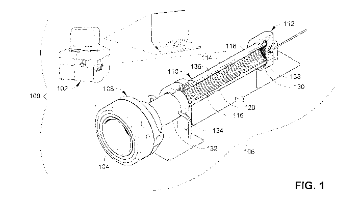
[0006] FIG. 1 is a diagrammatic illustration of an EVIS system that includes a
drift
chamber with a patterned resistive trace deposited on an interior surface of
the drift
chamber in accordance with an example implementation of the present
disclosure.
100071 FIG. 2 is a partial cross-sectional isometric view illustrating a drift
chamber
with a patterned resistive trace deposited on an interior surface of the drift
chamber in
accordance with an example implementation of the present disclosure.
CA 02907115 2015-09-16
WO 2014/146200
PCT/CA2014/050290
[0008] FIG. 3 is a partial cross-sectional isometric view illustrating a drift
chamber
with a helical resistive trace deposited on an interior surface of the drift
chamber in
accordance with an example implementation of the present disclosure, where
portions
of the drift chamber are shown in phantom to illustrate the helical pattern of
the
resistive trace.
100091 FIG. /1 is a diagrammatic illustration of a pattern for a resistive
trace deposited
on an interior surface of a charged material transportation chamber, such as
the drift
chamber illustrated in FIG. 2, where the resistive trace includes multiple
turns of more
than two hundred and seventy degrees (270') oriented at least substantially
perpendicular to a longitudinal axis of the charged material transportation
chamber,
and where adjacent turns of the resistive trace are connected to one another
in series
using jumpers deposited on an interior surface of the charged material
transportation
chamber in accordance with an example implementation of the present
disclosure.
100101 FIG. 5 is a diagrammatic illustration of a pattern for a resistive
trace deposited
on an interior surface of a charged material transportation chamber, such as
the drift
chamber illustrated in FIG. 2, where the resistive trace includes multiple
turns of less
than two hundred and seventy degrees (270') oriented at least substantially
perpendicular to a longitudinal axis of the charged material transportation
chamber,
and where adjacent turns of the resistive trace are connected to one another
in series
using jumpers deposited on an interior surface of the charged material
transportation
chamber in accordance with an example implementation of the present
disclosure.
100111 FIG. 6 is a partial cross-sectional isometric view illustrating a
charged material
transportation chamber with a patterned resistive trace deposited on an
exterior
surface of the charged material transportation chamber and/or a patterned
resistive
trace deposited on an interior surface of the charged material transportation
chamber
in accordance with an example implementation of the present disclosure.
100121 FIG. 7 is a flow diagram illustrating a method of manufacturing a
charged
material transportation chamber with a patterned resistive trace deposited on
an
interior surface and/or an exterior surface of the charged material
transportation
chamber in accordance with an example implementation of the present
disclosure.
100131 FIG. 8 is a partial cross-sectional isometric view illustrating a
charged material
transportation chamber with a helical resistive trace being deposited on an
interior
surface of the charged material transportation chamber, where the substrate is
advanced longitudinally at a first rate in accordance with an example
implementation
3
CA 02907115 2015-09-16
WO 2014/146200
PCT/CA2014/050290
of the present disclosure, and where a portion of the substrate is removed to
illustrate
the helical pattern of the resistive trace.
100141 FIG. 9 is a partial cross-sectional isometric view illustrating a
charged material
transportation chamber with a helical resistive trace being deposited on an
interior
surface of the charged material transportation chamber, where the substrate is
advanced longitudinally at a second rate in accordance with an example
implementation of the present disclosure, and where a portion of the substrate
is
removed to illustrate the helical pattern of the resistive trace.
100151 FIG. 10 is a partial cross-sectional isometric view illustrating a
charged
material transportation chamber with multiple helical resistive traces
deposited on an
interior surface of the charged material transportation chamber in accordance
with an
example implementation of the present disclosure, where a portion of the
substrate is
removed to illustrate the helical patterns of the resistive traces.
100161 FIG. 11A is a partial cross-sectional isometric view illustrating a
charged
material transportation chamber with multiple patterned resistive traces being
deposited on an interior surface of the charged material transportation
chamber in
accordance with an example implementation of the present disclosure, where a
portion of the substrate is removed to illustrate the patterns of the
resistive traces.
100171 FIG. 11B is a partial cross-sectional isometric view illustrating a
charged
material transportation chamber with multiple patterned resistive traces
deposited
longitudinally on an interior surface of the charged material transportation
chamber in
accordance with an example implementation of the present disclosure, where a
portion of the substrate is removed to illustrate the patterns of the
resistive traces.
100181 FIG. 12 is a partial cross-sectional isometric view illustrating a
charged
material transportation chamber with a patterned resistive trace being
deposited on an
interior surface of the charged material transportation chamber, where the
substrate is
advanced longitudinally at two different rates in accordance with an example
implementation of the present disclosure, and where a portion of the substrate
is
removed to illustrate the pattern of the resistive trace.
100191 FIG. 13A is a partial cross-sectional isometric view illustrating a
charged
material transportation chamber with a patterned resistive trace deposited on
an
interior surface of the charged material transportation chamber, where the
substrate is
advanced longitudinally at two different rates in accordance with an example
4
CA 02907115 2015-09-16
WO 2014/146200
PCT/CA2014/050290
implementation of the present disclosure, and where a portion of the substrate
is
removed to illustrate the pattern of the resistive trace.
100201 FIG. 13B is a partial cross-sectional isometric view illustrating a
charged
material transportation chamber with a patterned resistive trace deposited on
an
interior surface of the charged material transportation chamber, where the
substrate is
advanced longitudinally at two different rates in accordance with an example
implementation of the present disclosure, and where a portion of the substrate
is
removed to illustrate the pattern of the resistive trace.
10021] FIG. 14A is a partial cross-sectional isometric view illustrating a
charged
material transportation chamber with a patterned resistive trace deposited on
an
interior surface of the charged material transportation chamber, where the
substrate is
advanced longitudinally at two different rates in accordance with an example
implementation of the present disclosure, and where a portion of the substrate
is
removed to illustrate the pattern of the resistive trace.
10022] FIG. 14B is a partial cross-sectional isometric view illustrating a
charged
material transportation chamber with a patterned resistive trace deposited on
an
interior surface of the charged material transportation chamber, where the
substrate is
advanced longitudinally at two different rates in accordance with an example
implementation of the present disclosure, and where a portion of the substrate
is
removed to illustrate the pattern of the resistive trace.
100231 FIG. 15A is a partial cross-sectional isometric view illustrating a
charged
material transportation chamber with a secondary helical resistive trace
deposited on
an interior surface of the charged material transportation chamber, where the
secondary helical resistive trace is deposited over a primary resistive
coating in
accordance with an example implementation of the present disclosure, and where
a
portion of the substrate is removed to illustrate the pattern of the resistive
trace.
100241 FIG. 15B is a cross-sectional end view of the charged material
transportation
chamber illustrated in FIG. 15A.
[0025] FIG. 16 is a partial isometric view illustrating a charged material
transportation chamber with a patterned resistive trace deposited on an
interior surface
of the charged material transportation chamber in accordance with an example
implementation of the present disclosure, where a portion of the substrate is
removed
to illustrate the pattern of the resistive trace.
CA 02907115 2015-09-16
WO 2014/146200
PCT/CA2014/050290
100261 FIG. 17 is a partial cross-sectional isometric view illustrating a
charged
material transportation chamber with a series of concentric resistive traces
applied to
an interior surface of the charged material transportation chamber arid linked
by a
longitudinal resistive trace, where the longitudinal resistive trace is in
electrical
contact with opposite ends of the charged material transportation chamber in
accordance with an example implementation of the present disclosure, and where
a
portion of the substrate is removed to illustrate the patterns of the
resistive traces.
100271 FIG. 18 is an isometric view of the charged material transportation
chamber
illustrated in FIG. 17.
100281 FIG. 19 is a cross-sectional side elevation view of the charged
material
transportation chamber illustrated in FIG. 17.
100291 FIG, 20 is a diagrammatic illustration of multiple resistive traces
linked by a
longitudinal resistive trace in accordance with an example implementation of
the
present disclosure, further illustrating resistances of the multiple resistive
traces and
the longitudinal resistive trace.
DETAILED DESCRIPTION
10030] FIG. 1 is an illustration of a spectrometer system, such as an ion
mobility
spectrometer (IMS) system 100. Although IMS detection techniques are described
herein, it should be noted that a variety of different spectrometers can
benefit from the
structures, techniques, and approaches of the present disclosure. It is the
intention of
this disclosure to encompass and include such changes. IMS systems 100 can
include
spectrometry equipment that employs unheated (e.g., surrounding (ambient or
room)
temperature) detection techniques. For example, an IMS system 100 can be
configured as a lightweight explosive detector. However, it should be noted
that an
explosive detector is provided by way of example only and is not meant to be
restrictive of the present disclosure. Thus, techniques of the present
disclosure may
be used with other spectrometry configurations. For example, an IMS system 100
can
be configured as a chemical detector. Further, in other implementations, IMS
systems
100 can employ heated detection techniques. For example, an IMS system 100 can
be
configured as a gently heated detector, a fully heated detector, and so forth.
An IMS
system 100 can include a detector device, such as a sample detector 102,
having a
sample receiving port for introducing material (e.g., particles) from a sample
of
6
CA 02907115 2015-09-16
WO 2014/146200
PCT/CA2014/050290
interest to a reaction region/chamber. For example, the sample detector 102
can have
an inlet 104 where air to be sampled is admitted to the sample detector 102.
100311 In some implementations, the sample detector 102 can have another
device
such as a gas ehromatograph (not shown) connected in line with the inlet 104.
For
example, the 1MS system 100 can be configured for gas chromatography-ion
mobility
spectrometry (GC-IMS), where the sample detector 102 is coupled with the gas
chromatograph (GC) for common sample introduction (e.g., where a GC capillary
column is connected to the sample detector 102 with molecules ionized as they
elute
from the GC). However, gas chromatography is provided by way of example only
and is not meant to be restrictive of the present disclosure. Thus, the sample
detector
102 can be used with other detection instrumentation including, but not
necessarily
limited to: high-pressure liquid chromatography (HPLC), ion mobility
spectrometry-
mass spectrometry (IMS-MS) (e.g., with quadropole, time-of-flight, and/or
Fourier
transform cyclotron resonance techniques), liquid chromatography-ion mobility
spectrometry-mass spectrometry (LC-1MS-MS), and so forth.
[00321 Referring now to FIG. 2, the inlet 104 is defined by an ion detection
assembly
106. The ion detection assembly 106 includes an inlet assembly 108, a
reaction/ionization chamber (e.g., a reaction chamber 132), a gate 134, a
drift
chamber (e.g., a drift tube 110), and a collector assembly 112. The drift tube
110
and/or the reaction chamber 132 comprises a chamber (e.g., a tube 114) having
one or
more walls formed of substantially non-conductive (e.g., insulating) material
including, but not necessarily limited to: a ceramic material (e.g.,
kaolinite, aluminum
oxide, crystalline oxide, a nitride material, a carbide material, silicon
carbide, tungsten
carbide, and so forth), glass, porcelain, polymer, and/or a composite
material.
However, these materials are provided by way of example only and are not meant
to
be restrictive of the present disclosure. Thus, in other implementations, the
tube 114
can be constructed using other materials. For example, the tube 114 is
constructed of
semi-conductive material, which can provide a more uniform electric field
within the
tube 114 when used with a patterned resistive trace deposited on the inside of
the tube
114 (e.g., with respect to a tube constructed of insulating material). In
embodiments
of the disclosure, one or both of the drift chamber and the
reaction/ionization chamber
are configured as a charged material transportation chamber including a tube
114 as
7
CA 02907115 2015-09-16
WO 2014/146200
PCT/CA2014/050290
described herein. For example, in some embodiments, the drift tube 110
includes tube
114. In other embodiments, the reaction chamber 132 includes tube 114. In
still
further embodiments, the drift tube 110 and the reaction chamber 132 both
include a
tube 114 (e.g., each including a separate tube 114, both using the same tube
114, each
using portions of the same tube 114, and so forth). However, it should be
noted that
drift chambers and reaction/ionization chambers are provided by way of example
only
and are not meant to limit the present disclosure. In other embodiments, a
charged
material transportation chamber including a tube 114 is configured
differently.
100331 The tube 114 has an interior surface 116 and an exterior surface 118.
Either or
both ends of the tube 114 and/or one or more drift segments of the tube 114
are open
and allow material (e.g., vapor, particles, and so forth) to pass through the
tube 114.
A patterned resistive trace 120 is deposited on the interior surface 116
and/or the
exterior surface 118 of the tube 114. For example, a resistive trace 120 is
printed on
the interior surface 116 of the tube 114 and/or the exterior surface 118 of
the tube 114
using a conductive ink, a conductive paste, vacuum-deposition, electro-
deposition, a
chemical treatment, and so forth. In some instances, the drift tube 110
includes more
than one patterned resistive trace, such as a first resistive trace 120
printed on the
interior surface 116 of the tube 114 and a second resistive trace 120 printed
on the
exterior surface 118 of the tube 114. A patterned resistive trace provides
electrical
conductivity along the tube 114, including electrical conductivity at the
surface of the
tube 114 (e.g., at a patterned resistive trace deposited along the interior
surface 116
and/or the exterior surface 118 of the tube 114). Patterned resistive traces
can be
printed in various regions of an ion detection assembly 106, including, but
not
necessarily limited to: an inlet region, a reaction region, and so forth.
100341 As described herein, the resistive traces 120 provide a small active
internal
surface area (e.g., with respect to a typical stackable drift tube). Further,
a surface of
the tube 114 on which one or more of the resistive traces 120 is disposed is
at least
substantially free of gaps and/or cavities in which contaminants can
accumulate,
which could otherwise extend and/or complicate maintenance procedures on the
tube
114, such as cleaning cycles and so forth. The resistive traces 120 can
provide a
continuous, consistent, and/or substantially uniform temperature and/or
electric field
along the length of the tube 114. In embodiments of the disclosure, geometry
of a
CA 02907115 2015-09-16
WO 2014/146200
PCT/CA2014/050290
resistive trace 120 allows for a higher total resistance (e.g., as used in
high voltage
(HV) power supply implementations) with conductive trace material that has
comparatively lower resistivity and can provide better stability of surface
resistivity
over time. Further, in accordance with the present disclosure, the
configurations
described herein can reduce and/or minimize electric fields in a direction
generally
perpendicular to the longitudinal axis of the tube 114, while reducing and/or
minimizing penetration of external electrical fields into the interior of the
tube 114.
100351 As shown, a drift tube 110 can be of unitary construction, which can
provide
more reliability than, for example, a typical stackable drift tube
configuration.
Further, the drift tube 110 does not necessarily require an external housing,
thus
potentially reducing the costs associated with manufacturing and/or
maintenance of,
for example, a system 100. In example implementations, a drift tube 110 does
not
necessarily require an external heating element. For instance, a heating
element (e.g.,
one or more of the resistive traces 120) can be deposited onto the tube 114
(e.g.,
deposited on the exterior surface 118 of the tube 114) and function to
establish a
controlled (e.g., heated) temperature for the tube. Such configurations can
further
reduce the cost and/or complexity of manufacturing a system 100 as described
herein.
In some embodiments, a resistive trace 120 deposited on the exterior surface
118 of
the tube 114 is configured to produce similar electric potential as a
resistive trace 120
deposited on the interior surface 116 of the tube 114 (e.g., to provide
improved
uniformity of the electric field inside the tube 114).
100361 As shown in FIG. 3, a resistive trace 120 can be configured as a
helical
resistive trace with multiple turns deposited adjacent to one another on the
interior
surface 116 of the tube 114. As used herein, the term "turn" is associated
with the
partial or complete circumferential travel of a segment of a patterned
resistive trace
with respect to the interior surface 11 6 of the tube 114 and/or the exterior
surface 118
of the tube 114. In some implementations, a turn can be oriented at an angle
from a
perpendicular direction defined with respect to a longitudinal axis 126 of the
tube 114
(e.g., in the case of the helical resistive traces 120 shown in FIGS. 3 and
6). Further, a
turn can be oriented generally (e.g., at least substantially) perpendicular to
the
longitudinal axis 126 of the tube 114. For instance, as shown in FIGS. 4 and
5,
resistive traces 120 can be configured with multiple turns deposited adjacent
to one
9
CA 02907115 2015-09-16
WO 2014/146200
PCT/CA2014/050290
another on the interior surface 116 of the tube 114, where one or more of the
turns are
oriented at least substantially perpendicular to the longitudinal axis 126 of
the tube
114. A turn can be associated with complete circumferential travel of a
segment of a
patterned resistive trace with respect to the interior surface 116 of the tube
114 (e.g.,
as shown in FIG, 3) and/or the exterior surface 118 of the tube 114 (e.g., as
shown in
FIG. 6). A turn can also be associated with partial circumferential travel of
a segment
of a patterned resistive trace with respect to the interior surface 116 of the
tube 114
(e.g., as shown in FIG. 4 with turns of more than two hundred and seventy
degrees
(270 ) but less than three hundred and sixty degrees (360 ), and FIG. 5 with
turns of
less than two hundred and seventy degrees (270 )).
100371 In embodiments of the disclosure, the number of turns can vary (e.g.,
depending upon the geometry of a particular chamber, operating voltage
requirements, a desired uniformity for the generated electric field, and so
forth). For
example, a gap between adjacent turns of a resistive trace 120 may be limited
by
breakdown voltage. Further, the width of a resistive trace 120 can be
determined
based upon the angle between the resistive trace 120 and the longitudinal axis
126 of
the tube 114. For example, a resistive trace 120 with a larger width may be
used with
a larger angle between the resistive trace 120 and the longitudinal axis 126
and
produce a larger deflection of material trajectories. In this manner, gaps
between
turns/rings or their overlapping groups can be selected based upon a minimum
distance to reliably withstand operating voltage, and widths of turns/rings or
their
overlapping groups can be selected based upon a maximum width to maintain
substantial perpendicularity of the turns/rings or their overlapping groups
with respect
to the axis of the chamber. In one configuration, a resistive trace 120 can
include
eighteen (18) turns. In another configuration, a resistive trace 120 can
include thirty-
six (36) turns. In a further configuration, a resistive trace 120 can include
seventy-
two (72) turns. However, these configurations are provided by way of example
only
and are not meant to be restrictive of the present disclosure. Thus, in other
configurations, a resistive trace 120 can include fewer than eighteen (18)
turns,
between eighteen (18) turns and thirty-six (36) turns, between thirty-six (36)
turns and
seventy-two (72) turns, more than seventy-two (72) turns, and so forth,
CA 02907115 2015-09-16
WO 2014/146200
PCT/CA2014/050290
100381 In some implementations, each turn of a patterned resistive trace is
electrically
connected to an adjacent turn in series. For example, as shown in FIG. 3,
adjacent
turns of the helical resistive trace 120 are connected to one another on the
interior
surface 116 of the tube 114. Referring now to FIGS. 4 and 5 adjacent turns of
the
resistive trace 120 can also be connected together using one or more jumpers
128. As
shown in FIGS. 4 and 5, adjacent turns of the resistive trace 120 can be
connected
together using jumpers 128 deposited on the interior surface 116 of the tube
114.
10039.1 Referring generally to FIGS. 8 through 15B, an application tool can be
used to
apply various resistive trace patterns to the interior and/or exterior
surfaces of a non-
conductive or semi-concluetive tube. In embodiments of the disclosure,
relative
motion of the tube and the application tool can be varied to create different
resistive
patterns. For example, as shown in FIG. 8, a conductive ink or film resistive
trace
120 is applied to the interior surface 1 I 6 and/or the exterior surface 118
of the tube
114 by rotating the tube 114 at a controlled (e.g., at least substantially
constant) rate,
while the tube 114 is advanced longitudinally (e.g., horizontally) with
respect to a
stationary, or at least substantially stationary, application tool such as an
ink
application stylus 122. The motion of the tube 114 with respect to the ink
application
stylus 122 creates a pattern on the interior surface 116 and/or the exterior
surface 118
of the tube 114.
100401 As described herein, terms that refer to motion of the tube 114 and/or
the ink
application stylus 122, such as "rotating," "advancing," and so forth, are
used to
describe relative motion of the tube 114 with respect to the ink application
stylus 122,
Thus, in some embodiments, the tube 114 is rotated while the ink application
stylus
122 is advanced. In other embodiments, the ink application stylus 122 is
rotated
while the tube 114 is advanced. In further embodiments, the tube 114 and the
ink
application stylus 122 are both rotated while one or both are advanced, In
still further
embodiments, the tube 114 and the ink application stylus 122 are both advanced
while
one or both are rotated. In further embodiments, the ink application stylus
122 is
rotated and advanced while the tube 114 remains stationary, or at least
substantially
stationary, and so forth,
11
CA 02907115 2015-09-16
WO 2014/146200
PCT/CA2014/050290
100411 Different speeds and/or motion sequences for the tube 114 and/or the
ink
application stylus 122 are used to create different patterns on the tube 114.
With
reference to FIG. 9, a patterned resistive trace comprising a continuous
conductive
coating 124 is established between opposite ends of the tube 114 by rotating
the tube
114 at a controlled rate while longitudinal motion of the tube 114 is very
slow with
respect to the rotational motion of the tube 114. This difference in the
relative speeds
of rotation and longitudinal motion creates a tightly wound conductive spiral.
In
some embodiments, adjacent segments of a resistive trace 120 overlap,
resulting in the
continuous conductive coating 124 on the interior surface 116 and/or the
exterior
surface 118 of the tube 114. Conductive inks and/or films with sufficiently
high
resistance can be deposited in this configuration to achieve a particular
total drift tube
resistance.
100421 As shown in FIG. 10, multiple helical resistive traces 120 can be
established
on the tube 114 by repositioning the application tool at an end of the tube
114 at
ninety degrees (90 ), or another division of three hundred and sixty degrees
(360 ),
with respect to the origin of a previous resistive trace 120 at the end of the
tube 114.
This technique can be used to create multiple resistive traces 120
substantially parallel
to one another. In embodiments of the disclosure, the substantially parallel
resistive
traces 120 are used to provide greater symmetry at ends of the tube 114 (e.g.,
with
respect to a single resistive trace 120).
100431 Referring to FIGS. I IA and 11B, multiple resistive traces 120 can be
generated between ends of the tube 114. As shown in FIG. 11A, rotation of the
tube
114 at a controlled (e.g., at least substantially constant) rate, with
longitudinal motion
at a relatively higher rate in a first direction, creates a slightly curved
resistive trace
120 between the opposite ends of the tube 114. Then, longitudinal motion of
the tube
114 in a second, opposite direction is used to establish another consecutive
and
somewhat parallel resistive trace 120 between the opposite ends of the tube
114. In
this manner, a series of generally parallel resistive traces 120 are deposited
between
the ends of the tube 114. In other embodiments, parallel resistive traces 120
are
established between opposite ends of the tube 114 (e.g., as shown in FIG.
11B). In
embodiments of the disclosure, these techniques can be used to provide more
12
CA 02907115 2015-09-16
WO 2014/146200
PCT/CA2014/050290
consistent electrical connection between the ends of the tube 114 (e.g., with
respect to
a single resistive trace 120).
100441 As shown in FIG. 12, various patterns of trace configurations, such as
the trace
patterns shown in FIGS. 8 through 11, can be implemented together. In these
configurations, rotation of the tube 114 at a controlled (e.g., at least
substantially
constant) rate with relatively slower longitudinal motion for a first period
of time
results in a turn of a resistive trace 120. The longitudinal motion of the
tube 114 may
also be stopped during the first period of time. This motion is followed by
continued
rotation of the tube 114 at the controlled rate with relatively faster
longitudinal motion
for a second (e.g., shorter) period of time, resulting in a single, slightly
curved jumper
128. The rotation of the tube 114 may also be stopped during the second period
of
time, resulting in a substantially linear jumper 128. Then, rotation of the
tube 114 at
the controlled rate, with longitudinal motion at the relatively slower rate,
results in
another turn of the resistive trace 120. Again, this motion is followed by
generation
of another jumper 128, another turn of the resistive trace 120, and so on. In
this
manner, alternating sequences of slow andlor stopped, and relatively faster
longitudinal motion of the tube 114 results in a series of turns of a
resistive trace 120,
connected to one another along the longitudinal axis 126 of the tube 114 with
jumpers
128. In some embodiments, coaxial resistive turn portions of a resistive trace
120 are
deposited using other methods, including but not necessarily limited to vacuum
deposition, prior to using the ink application stylus 122 to deposit one or
more
jumpers 128 along the length of the tube 114 to connect the coaxial turn
portions and
increase the uniformity of the total resistance across the tube 114.
100451 As shown in FIGS. 13A and 13B, additional combinations of the above
approaches can be implemented in the form of a tightly wound patterned
resistive
trace comprising a continuous conductive coating 424 deposited at a
comparatively
slower longitudinal speed alternating with connecting jumpers 128 deposited at
a
comparatively higher longitudinal speed. FIG 13A depicts two continuously
coated
portions connected with a single conductive jumper 128. FIG 13B depicts
several
brief continuously coated portions connected with multiple jumpers 128. In
some
embodiments, e.g., to achieve at least substantial field uniformity, the width
of the
continuously coated portion and/or the width of a gap between the continuously
13
CA 02907115 2015-09-16
WO 2014/146200
PCT/CA2014/050290
coated portions are configured to approximate a particular pattern, such as
the pattern
described with reference to FIG. 12. In embodiments of the disclosure, the
patterned
resistive traces described in FIGS. 13A and 13B can be used to create a
stepped
electric field for moving ions, where each jumper 128 creates a resistive drop
between
adjacent portions of the continuous conductive coating 124. For example, a
voltage
drop can be created between adjacent continuously coated portions by the
higher
resistance of a jumper 128 with respect to the continuous conductive coating
124
(e.g., due to the reduced cross-sectional area of the jumper 128 with respect
to the
continuous conductive coating 124). Further, the patterned resistive traces
call be
applied using a resistive ink via high pressure delivery through an
application tool,
such as a stainless steel needle. The motion of the tube 114 and/or the
application
tool can be controlled using, for example, one or more stepper motors.
100461 Referring now to FIGS. 14A and 14B, additional combinations of
previously
described approaches can be implemented in the form of a patterned resistive
trace
comprising loosely wound helical resistive traces 120, which can be deposited
at a
moderate longitudinal speed alternating with jumpers 128. FIG. 14A depicts two
large helical resistive trace portions connected with jumpers 128. FIG. 14B
depicts
several brief helical resistive trace portions connected with jumpers 128.
[00471 As shown in FIGS. 15A and 1513, the tube 114 can also have a primary
continuous conductive coating 140 applied on its interior surface 116 and/or
exterior
surface 118, over which a secondary resistive trace 120 can be applied. The
secondary resistive trace 120 can be helical or any combination of patterns
depicted
in, for instance, the preceding figures. In this configuration, one or more
resistive
traces 120 can reduce and/or minimize electric field distortions caused by
resistive
and/or physical imperfections in the uniformity of the primary continuous
conductive
coating 140. Further, the primary continuous conductive coating 140 can reduce
and/or minimize the influence of external electric fields on the interior of
the tube
114, which acts as the drift region 136. In some embodiments, the total
resistance of
the primary continuous conductive coating 140 across the tube 114 is greater
than the
resistance of the secondary resistive trace 120. For example, the resistance
of the
primary continuous conductive coating 140 can be about five hundred mega ohms
14
CA 02907115 2015-09-16
WO 2014/146200
PCT/CA2014/050290
(500 MS2), and the resistance of the resistive trace 120 can range between
about
twenty mega ohms (20 MC2) and two hundred mega ohms (200 MQ).
100481 Referring now to FIG. 16, in some embodiments the tube 114 includes a
patterned resistive layer 142 comprising one or more apertures (e.g., slots
144)
oriented in directions generally (e.g., at least substantially) perpendicular
to the
longitudinal axis 126 of the tube 114. In embodiments of the disclosure, the
apertures
are configured to reduce or minimize radial electric field caused by potential
electrical
asymmetry of, for instance, a continuous layer. In the configuration shown in
FIG.
16, the slots 144 are axially interleaved. However, this configuration is
provided by
way of example only and is not meant to limit the present disclosure. In other
embodiments, the slots 144 can be shaped and/or aligned differently.
100491 In some embodiments a tube 114 has multiple resistive traces 120 (e.g.,
conductive rings) applied to its interior surface 116 and/or exterior surface
118, and
the resistive traces 120 are linked (e.g., connected) using one or more
longitudinal
resistive traces 146, For example, as shown in FIGS. 17 through 20, resistive
traces
120 configured as a series of concentric resistive ink rings are applied to
the interior
surface 116 of the tube 114. The resistive traces 120 are then linked by a
longitudinal
resistive trace 146 configured as a generally straight, longitudinal resistive
ink trace
connected between, for example, two connectors 130 disposed on the tube 114.
For
example, the longitudinal resistive trace 146 is in electrical contact with
metalized
ends of the tube 114. However, it should be noted that the concentric
resistive ink
rings and the generally straight, longitudinal resistive ink trace are
provided by way of
example only and are not meant to limit the present disclosure. In other
embodiments, differently configured resistive traces 120 and/or longitudinal
resistive
traces 146 are used. For example, a longitudinal resistive trace 146 can be
slightly
curved, sinusoidal, and so forth. Further, one or more of the resistive traces
120 can
be helical or any combination of patterns depicted in, for instance, the
preceding
figures.
100501 In some embodiments, the resistivity of the ink comprising the
concentric
rings is greater than (e.g., substantially greater than) the resistivity of
the ink
comprising the straight, continuous trace. For example, the total resistance
of the
CA 02907115 2015-09-16
WO 2014/146200
PCT/CA2014/050290
generally straight, longitudinal resistive ink trace on its own is about one
hundred
mega ohms (100 Mt2). This configuration can be used to reduce (e.g., minimize)
the
effect of the additional parallel resistance applied across the generally
straight,
longitudinal resistive ink trace (e.g., as shown in FIG. 20). However, this
resistance
value is provided by way of example only and is not meant to limit the present
disclosure. In other embodiments, the total resistance of the generally
straight,
longitudinal resistive ink trace can be greater than or less than about one
hundred
mega ohms.
100511 In some configurations, one or more patterned resistive traces
deposited on an
exterior surface 118 of the tube 114 are electrically connected to one or more
patterned resistive traces deposited on an interior surface 116 of the tube
114. For
example, jumpers 128 can be used to connect a resistive trace 120 deposited on
the
interior surface 116 of the tube 114 to one or more resistive traces 120
deposited on
the exterior surface 118 of the tube 114 (e.g., connected in series). However,
this
configuration is provided by way of example only and is not meant to be
restrictive of
the present disclosure. In other implementations, one or more resistive traces
120
deposited on the exterior surface 118 of the tube 114 and one or more
resistive traces
120 deposited on the interior surface 116 of the tube 114 are separately
connected
(e.g., connected in parallel).
10052.1 In some configurations, the length of the tube 114 is between at least
approximately two centimeters (2 cm) and fifteen centimeters (15 cm). The
diameter
of the interior surface 116 of the tube 114 can be between at least
approximately two
and one-half millimeters (2.5 mm) and twenty-five millimeters (25 mm).
Further, the
diameter of the exterior surface 118 of the tube 114 can be between at least
approximately three millimeters (3 mm) and thirty millimeters (30 mm).
However,
these dimensions are provided by way of example only and are not meant to be
restrictive of the present disclosure. Thus, in other configurations, the
length of the
tube 114 may be less than at least approximately two centimeters (2 cm) or
greater
than at least approximately fifteen centimeters (15 cm). The diameter of the
interior
surface 116 of the tube 114 may be less than at least approximately two and
one-half
millimeters (2.5 mm) or greater than at least approximately twenty-five
millimeters
(25 mm). Further, the diameter of the exterior surface 118 of the tube 114 may
be
16
CA 02907115 2015-09-16
WO 2014/146200
PCT/CA2014/050290
less than at least approximately three millimeters (3 mm) or greater than at
least
approximately thirty millimeters (30 mm).
100531 The width of a patterned resistive trace (e.g., as measured in a
generally
longitudinal direction parallel to the longitudinal axis 126 of the tube 114)
can be
between at least approximately one-tenth of one millimeter (0.1 mm) and one
millimeter (1 mm). For example, the width of the resistive trace 120 can be at
least
approximately twenty one-thousandths of one inch (0.020"). In some
configurations,
the resistive trace 120 has at least approximately two turns per centimeter.
For
example, the pitch of a patterned resistive trace, which can be defined as the
spacing
between the centerlines of the deposited material forming adjacent turns of
the
patterned resistive trace, can be between at least approximately one-tenth of
one
millimeter (0,1 mm) and one millimeter (1 mm). For example, the pitch of the
resistive trace 120 can be at least approximately twenty-eight one-thousandths
of one
inch (0.028"). However, these dimensions are provided by way of example only
and
are not meant to be restrictive of the present disclosure. Thus, in other
configurations,
the width of a patterned resistive trace can be less than at least
approximately one-
tenth of one millimeter (0.1 mm) or greater than one millimeter (1 mm). The
resistive
trace 120 can have more or fewer than at least approximately two turns per
centimeter. Further, the pitch of a patterned resistive trace can be less than
at least
approximately one-tenth of one millimeter (0.1 mm) or greater than at least
approximately one millimeter (1 mm).
100541 In some instances, one or more characteristics of the resistive traces
120 can
be generally consistent throughout the length of the tube 114. For example,
the pitch
of the resistive trace 120 can be generally constant throughout the length of
the tube
114. In other instances, one or more characteristics of the resistive traces
120 can
vary throughout the length of the tube 114, For instance, the pitch between
adjacent
turns of a patterned resistive trace can vary through the tube 114 (e.g.,
increasing
and/or decreasing). The width and/or thickness of a patterned resistive trace
can also
vary throughout the length of the tube 114.
100551 One or more of the resistive traces 120 is configured to connect to a
source of
electrical energy to energize the resistive trace and establish an electric
field. For
17
CA 02907115 2015-09-16
WO 2014/146200
PCT/CA2014/050290
example, one or more of the resistive traces 120 are formed using thick film
deposition to form an electrically resistive conductor. In some
implementations,
when energized, a substantially uniform electric field is established within
the tube
114. In implementations, the electric field is a high voltage (HV) electric
field, which
can be used to control movement of ionized materials through the tube 114
(e.g., in
the manner of a drift region/chamber). However, a substantially uniform
electric field
is provided by way of example only and is not meant to be restrictive of the
present
disclosure. For example, a shaped electric field can be established within the
tube
114. In an example implementation, the shaped electric field varies in
intensity (e.g.,
varying from lower intensity to higher intensity) along the length of the tube
114. In
some implementations, one or more of the resistive traces 120 can be an ion
modifier,
which can he used to separate ions that would otherwise have similar mobility.
For
instance, one or more resistive traces 120 configured as an ion modifier can
be used to
fragment ions and alter the mobility of the ions, the mass to charge ratio of
the ions,
and so forth.
100561 One or both ends of the drift tube 110 can include a connector 130. For
example, an end of the drift tube 110 can be capped with a flange coated with
conductive material (e.g., a metalized conductive flange). One or more of the
resistive traces 120 can electrically connect to the connector 130, which can
be
connected to a source of electrical energy (e.g., a power supply) to energize
a resistive
trace and establish an electric field. However, a conductive flange is
provided by way
of example only and is not meant to be restrictive of the present disclosure,
hi other
implementations, one or more of the resistive traces 120 can be connected to a
source
of electrical energy using other connectors including, but not necessarily
limited, to a
conductive cap, a conductive coating, and so forth. When energized, the drift
tube
110 can be used to provide controllable transportation of charged materials
(e.g., ions)
from one end of the drift tube 110 to the other end of the drift tube 110.
100571 The inlet 104 can employ a variety of sample introduction approaches.
In
some instances, a flow of air can be used. In other instances, IMS systems 100
can
use a variety of fluids and/or gases to draw material into the inlet 104.
Approaches
for drawing material through the inlet 104 include the use of fans,
pressurized gases, a
vacuum created by a drift gas flowing through a drift region/chamber, and so
forth.
18
CA 02907115 2015-09-16
WO 2014/146200
PCT/CA2014/050290
For example, the sample detector 102 can be connected to a sampling line,
where air
from the surrounding environment (e.g., room air) is drawn into the sampling
line
using a fan. IMS systems 100 can operate at substantially ambient pressure,
although
a stream of air or other fluid can he used to introduce sample material into a
reaction
region. In other instances, IMS systems 100 can operate at lower pressures
(i.e.,
pressures less than ambient pressure). Further, IMS systems l 00 can include
other
components to furnish introduetion of material from a sample source. For
example, a
dcsorbcr, such as a heater, can be included with an IMS system 100 to cause at
least a
portion of a sample to vaporize (e.g., enter its gas phase) so the sample
portion can be
drawn into the inlet 104. For instance, a sample probe, a swab, a wipe, or the
like, can
be used to obtain a sample of interest from a surface. The sample probe can
then be
used to deliver the sample to the inlet 104 of an INS system 100. IMS systems
100
can also include a pre-concentrator to concentrate or cause a bolus of
material to enter
a reaction region.
[00581 A portion of a sample can be drawn through an inlet 104 configured as a
small
aperture inlet (e.g., a pinhole) into the sample detector 102 using, for
example, a
diaphragm in fluid communication with an interior volume of the sample
detector
102. For instance, when the internal pressure in the interior volume is
reduced by
movement of the diaphragm, a portion of the sample is transferred from the
inlet 104
into the sample detector 102 through the pinhole. After passing through the
pinhole,
the sample portion enters the inlet assembly 108. The inlet assembly 108 can
include
a reaction chamber 132 where the sample is ionized using an ionization source,
such
as a corona discharge ionizer (e.g., having a corona discharge point), and
possibly
modified (e.g., using one or more reactants). However, a corona discharge
ionizer is
provided by way of example only and is not meant to be restrictive of the
present
disclosure. Other example ionization sources include, but are not necessarily
limited
to: radioactive and electrical ionization sources, such as a photoionization
source, an
electrospray source, a matrix assisted laser desorption ionization (MALDI)
source, a
nickel-63 source (63Ni), an americium-241 source (241Am), and so forth. In
some
instances, the ionization source can ionize material from a sample of interest
in
multiple steps. For example, the ionization source can generate a corona that
ionizes
gases in the reaction chamber 132 that are subsequently used to ionize the
material of
19
CA 02907115 2015-09-16
WO 2014/146200
PCT/CA2014/050290
interest. Example gases include, but are not necessarily limited to: nitrogen,
water
vapor, gases included in air, and so forth.
[0059] In implementations, the inlet assembly 108 can operate in positive
mode,
negative mode, switch between positive and negative mode, and so forth. For
example, in positive mode the ionization source can generate positive ions
from a
sample of interest, while in negative mode the ionization source can generate
negative
ions. Operation of the inlet assembly 108 in positive mode, negative mode, or
switching between positive and negative mode can depend on implementation
preferences, a predicted sample type (e.g., explosive, narcotic, toxic
industrial
chemicals), and so forth. Further, the ionization source can be pulsed
periodically
(e.g., based upon sample introduction, gate opening, the occurrence of an
event, and
so on).
100601 The sample ions can then be directed toward a gating assembly using an
electric field (e.g., generated in the same way or a similar way as in the
drift chamber
previously described). The gating assembly includes one or more (e.g., two)
gating
grids and can be opened momentarily to allow small clusters of sample ions to
enter a
drift region. For example, the inlet assembly 108 can include an electronic
shutter or
gate 134 at the inlet end of a drift region 136. In implementations, the gate
134
controls entrance of ions to the drift region 136. For example, the gate 134
can
include a mesh of wires to which an electrical potential difference is applied
or
removed. The drift region 136 has electrodes (e.g., focusing rings formed by
one or
more of the resistive traces 120) spaced along its length for producing an
electric field
to draw ions along the drift region 136 and/or to direct the ions toward a
detector
disposed generally opposite the gate 134 in the drift region 136. For example,
the
drift region 136, including the electrodes, can create a substantially uniform
field in
the drift region 136. The sample ions can be collected at a collector
electrode, which
can be connected to analysis instrumentation for analyzing the flight times of
the
various sample ions. For instance, a collector plate 138 at the far end of the
drift
region 136 can collect ions that pass along the drift region 136.
100611 The drift tube 110 can be used to separate ions admitted to the drift
region 136
based on the individual ions' ion mobility. Ion mobility is determined by the
charge
CA 02907115 2015-09-16
WO 2014/146200
PCT/CA2014/050290
on an ion, an ion's mass, geometry, and so forth. In this manner, EMS systems
100
can separate ions based on time of flight. The drift region 136 can have a
substantially uniform electrical field that extends from the gate 134 to a
collector.
The collector can be a collector plate 138 (e.g., a Faraday plate) that
detects ions
based on their charge as they contact the collector plate 138. In
implementations, a
drift gas can be supplied through the drift region 136 in a direction
generally opposite
the ions' path of travel to the collector plate 138. For example, the drift
gas can flow
from adjacent the collector plate 138 toward the gate 134. Example drift gases
include, but are not necessarily limited to: nitrogen, helium, air, air that
is re-
circulated (e.g., air that is cleaned and/or dried) and so forth. For example,
a pump
can be used to circulate air along the drift region 136 against the direction
of flow of
ions. The air can be dried and cleaned using, for instance, a molecular sieve
pack.
100621 In implementations, the sample detector 102 can include a variety of
components to promote identification of a material of interest. For example,
the
sample detector 102 can include one or more cells containing a calibrant
and/or a
dopant component. Calibrant can be used to calibrate the measurement of ion
mobility. Dopant can be used to selectively ionize molecules. Dopant can also
be
combined with a sample material and ionized to form an ion that can be more
effectively detected than an ion that corresponds to the sample material
alone. Dopant
can be provided to one or more of the inlet 104, the reaction chamber 132,
and/or the
drift region 136. The sample detector 102 can be configured to provide dopant
to
different locations, possibly at different times during operation of the
sample detector
102. The sample detector 102 can be configured to coordinate dopant delivery
with
operation of other components of an IlvIS system 100.
100631 A controller can detect the change in charge on the collector plate 138
as ions
reach it. Thus, the controller can identify materials from their corresponding
ions. In
implementations, the controller can also be used to control opening of the
gate 134 to
produce a spectrum of time of flight of the different ions along the drift
region 136.
For example, the controller can be used to control voltages applied to the
gate 134.
Operation of the gate 134 can be controlled to occur periodically, upon the
occurrence
of an event, and so forth. For example, the controller can adjust how long the
gate
134 is open and/or closed based upon the occurrence of an event (e.g., corona
21
CA 02907115 2015-09-16
WO 2014/146200
PCT/CA2014/050290
discharge), periodically, and so forth. Further, the controller can switch the
electrical
potential applied to the gate 134 based upon the mode of the ionization source
(e.g.,
whether the inlet assembly 108 is in positive or negative mode). In some
instances,
the controller can be configured to detect the presence of explosives and/or
chemical
agents and provide a warning or indication of such agents on an indicator.
100641 In implementations, an IMS system 100, including some or all of its
components, can operate under computer control. For example, a processor can
be
included with or in an IMS system 100 to control the components and functions
of
IMS systems 100 described herein using software, firmware, hardware (e.g.,
fixed
logic, circuitry), manual processing, or a combination thereof. The terms
"controller"
"functionality," "service," and "logic" as used herein generally represent
software,
firmware, hardware, or a combination of software, firmware, or hardware in
conjunction with controlling the IMS systems 100. In the ease of a software
implementation, the module, functionality, or logic represents program code
that
performs specified tasks when executed on a processor (e.g., CPU or CPUs). The
program code may be stored in one or more computer-readable memory devices
(e.g.,
internal memory and/or one or more tangible media), and so on. The structures,
functions, approaches, and techniques described herein can be implemented on a
variety of commercial computing platforms having a variety of processors.
10065] For example, the sample detector 102 may be coupled with the controller
for
controlling the energy supplied to the resistive traces 120. The controller
may include
a processing module, a communications module, and a memory module. The
processing module provides processing functionality for the controller and may
include any number of processors, micro-controllers, or other processing
systems, and
resident or external memory for storing data and other information accessed or
generated by the controller. The processing module may execute one or more
software programs, which implement techniques described herein. The processing
module is not limited by the materials from which it is formed or the
processing
mechanisms employed therein, and as such, may be implemented via
semiconductor(s) and/or transistors (e.g., using electronic integrated circuit
(IC)
components), and so forth. The communications module is operatively configured
to
communicate with components of the sample detector 102. The communications
22
CA 02907115 2015-09-16
WO 2014/146200
PCT/CA2014/050290
module is also communicatively coupled with the processing module (e.g., for
communicating inputs from the sample detector 102 to the processing module).
The
communications module and/or the processing module can also be configured to
communicate with a variety of different networks, including, but not
necessarily
limited to: the Internet, a cellular telephone network, a local area network
(LAN), a
wide area network (WAN), a wireless network, a public telephone network, an
Intranet, and so on.
100661 The memory module is an example of tangible computer-readable media
that
provides storage functionality to store various data associated with operation
of the
controller, such as software programs and/or code segments, or other data to
instruct
the processing module and possibly other components of the controller to
perform the
steps described herein, Thus, the memory can store data, such as a program of
instructions for operating the IMS system 100 (including its components),
spectral
data, and so on. Although a single memory module is shown, a wide variety of
types
and combinations of memory (e.g., tangible memory, non-transitory) may be
employed. The memory module may be integral with the processing module, may
include stand-alone memory, or may be a combination of both.
100671 The memory module may include, but is not necessarily limited to:
removable
and non-removable memory components, such as Random Access Memory (RAM),
Read-Only Memory (ROM), Flash memory (e.g., a Secure Digital (SD) memory card,
a mini-SD memory card, and/or a micro-SD memory card), magnetic memory,
optical
memory, Universal Serial Bus (USB) memory devices, hard disk memory, external
memory, and other types of computer-readable storage media. In
implementations,
the sample detector 102 and/or memory module may include removable Integrated
Circuit Card (ICC) memory, such as memory provided by a Subscriber Identity
Module (SIM) card, a Universal Subscriber Identity Module (L:SIM) card, a
Universal
Integrated Circuit Card (UICC), and so on.
100681 In implementations, a variety of analytical devices can make use of the
structures, techniques, approaches, and so on described herein. Thus, although
IMS
systems 100 are described herein, a variety of analytical instruments may make
use of
the described techniques, approaches, structures, and so on. These devices may
be
23
CA 02907115 2015-09-16
WO 2014/146200
PCT/CA2014/050290
configured with limited functionality (e.g., thin devices) or with robust
functionality
(e.g., thick devices). Thus, a device's functionality may relate to the
device's
software or hardware resources, e.g., processing power, memory (e.g., data
storage
capability), analytical ability, and so on.
Example Process
100691 The following discussion describes example techniques for fabricating a
charged material transportation chamber by depositing one or more patterned
resistive
traces on one or more of' an interior surface or an exterior surface of a non-
conductive
or semi-conductive tube, FIG. 7 depicts a process 700, in an example
implementation, for fabricating a charged material transportation chamber,
such as the
example drift tube 110 illustrated in FIGS. 1 through 6 and described above.
10070.1 In the process 700 illustrated, a patterned resistive trace is
deposited on one or
more of an interior surface or an exterior surface of a tube formed of
substantially
non-conductive material and/or semi-conductive material (Block 710). For
example,
with reference to FIGS. 1 through 6, resistive trace 120 is deposited on
interior
surface 116 of tube 114 and/or exterior surface 118 of tube 114. The resistive
trace
120 may be deposited (e.g., printed) on the interior surface 116 of the tube
114 and/or
the exterior surface 118 of the tube 114 as described in United States Patent
Publication Number 2008/0278278, filed July 21, 2008, and titled "FINE LINE
THICK FILM RESISTORS BY PHOTOLITHOGRAPHY;" United States Patent
Number 7,224,258, issued May 29, 2007, and titled, "Fine line thick film
resistors by
photolithography;" United States Patent Publication Number 2007/0262846, filed
May 4, 2007, and titled, "FINE LINE THICK FILM RESISTORS BY
PHOTOLITHOGRAPHY;" United States Patent Publication Number 2010/0209318,
filed April 28, 2010, and titled, "MICROFLUIDIC DEVICES FABRICATED BY
DIRECT THICK FILM WRITING AND METHODS THEREOF;" United States
Patent Number 7,736,592, issued June 15, 2010, and titled "Microtluidic
devices
fabricated by direct thick film writing and methods thereof;" United States
Patent
Publication Number 2011/0277803, filed March 18, 2011, and titled,
"THERMOCOUPLE DEVICE;" and/or United States Patent Number 4,485,387,
issued November 27, 1984, and titled, "Inking system for producing circuit
patterns,"
which are herein incorporated by reference in their entireties.
24
CA 02907115 2015-09-16
WO 2014/146200
PCT/CA2014/050290
[00711 In some implementations, a jumper is deposited on one or more of the
interior
surface or the exterior surface of the tube to connect adjacent turns of the
patterned
resistive traces together (Block 712). For instance, with continuing reference
to
FIGS. 1 through 6, jumpers 128 can be used to connect adjacent turns of
resistive
trace 120 together. In some implementations, another patterned resistive trace
is
deposited on one or more of the interior surface or the exterior surface of
the tube
(Block 720). For example, with continuing reference to FIGS. I through 6, a
second
resistive trace 120 is deposited on exterior surface 118 of tube 114. As
described,
resistive traces 120 are configured to connect to a source of electrical
energy to
establish an electric field (e.g., a substantially uniform electric field, a
shaped electric
field, and so forth) within tube 114 v'hen energized. In some implementations,
the
patterned resistive trace is connected to a connector of the tube, which is
configured
to connect the patterned resistive trace to the source of electrical energy
(Block 730).
For instance, with continuing reference to FIGS. 1 through 6, connector 130
can be
formed to connect to resistive traces 120. As described, connector 130 can be
formed
as a conductive flange, a conductive cap, a conductive coating, and so forth.
Connector 130 can then be connected to a source of electrical energy (e.g., a
power
supply) to energize a patterned resistive trace and establish an electric
field.
100721 Although the subject matter has been described in language specific to
structural features and/or methodological acts, it is to be understood that
the subject
'natter defined in the appended claims is not necessarily limited to the
specific
features or acts described. Although various configurations are discussed,
the
apparatus, systems, subsystems, components and so forth can be constructed in
a
variety of ways without departing from this disclosure. Rather, the specific
features
and acts are disclosed as example forms of implementing the claims.
-75