Note: Descriptions are shown in the official language in which they were submitted.
CA 02907223 2015-09-15
WO 2014/143956
PCT/US2014/028158
HIGH FREQUENCY MIXER, METHOD AND SYSTEM
[ton] Related Applications
[0002] This application is a continuation of U.S. patent application serial
number
13i840,816 filed March 15, 2013, which is herein incorporated by reference in
its entirety.
[0003] Field of the Invention
[0004] The invention relates generally to radio transmitters utilizing a mixer
to produce an
output signal of a given frequency. In particular, the invention relates to
circuits containing
mixers that combine a first signal LO with a second signal RF to yield a third
signal IF,
especially in a relatively high-frequency application. More particularly, this
invention
relates to such circuits for use in satellites.
[0005] Background of the Invention
[0006] A common way to combine two input signals to produce an output signal
is to
employ a mixer. A key feature of a mixer circuit is one or more mixing
elements, which
generally comprise a nonlinear device such as a diode, field effect
transistor, or bipolar
junction transistor.
[0007] Mixing elements combine two frequency inputs to yield other frequency
outputs,
which vary according to the features of the particular mixing elements. In
particular, mixing
elements are designed to output second order frequencies, which include the
sum and
difference of the two input signal frequencies. In COMMOn usage, an LO signal
and an RF
signal enter the mixer element, which then outputs an IF signal that is either
the sum or
difference of the input frequencies.
[0008] In telecommunications, mixers receive a radio frequency input signal
(RF) and a
signal from a local oscillator (LO), and combine them to produce an output
signal. The
output signal comprises the Intermediate Frequency signal (IF) at a frequency
that is either
the difference or the total of the frequencies of the RF and LO signals. The
IF signal is
typically the useful or desired portion of the output signal, and it carries
the information of
the RF signal a different desired frequency.
-1-
CA 02907223 2015-09-15
WO 2014/143956
PCT/US2014/028158
[0009] Because mixers are non-linear, mixers output additional signals with
frequencies
other than the desired IF signal. The additional frequencies are various other
combinations
of the RF and LO frequencies, typically multiples of the RF or LO frequencies,
or sums and
differences of multiples of the input signal frequencies. These mixer by-
products are
referred to as spurious frequencies (-spurs"), or collectively as
interrnodulation distortion
(IMD). Typically these other frequency outputs are unwanted, and serve only as
noise or
interference.
[0010] In addition, depending on the frequencies of the RF, LO and IF signals,
the spurs
may be very close to the frequencies of the output signal. As an example, a
potential
problem encountered can be seen in the graph of FIG. 4, which shows the inputs
and some
of the outputs of a mixer. The mixer receives a radio-frequency (RF) input
signal 201 at a
frequency of 30 GHz and a local oscillator (LO) signal 202 with a frequency of
9.5 GHz.
The mixer produces spurs as multiples of the LO frequency and an intermediate
frequency
(IF) signal 203 with a frequency that is the difference between the
frequencies of RF signal
201 and LO signal 202, i.e., 30 GHz - 9.5 GHz = 20.5 GHz. However, one of the
spurs
produced by the mixer is a harmonic signal 204 of the LO signal 202, with a
frequency two
times the LO frequency, i.e., 2 x 9.5 GHz - 19 GHz. This is fairly close to
the IF frequency
of 20_5 GHz.
[0011] A common method to reduce the spurious output of the mixer while
retaining the
desired IF signal is to exclude the unwanted frequencies through the use of
high- or low-
pass filters, either alone or together as band-pass or notch filters, that
filter out some of the
spurs but let the desired frequency pass.
[0012] However, in the example, the two frequencies are so close that to try
to filter out the
2 x LO spur and pass the IF signal is difficult. In addition, the use of one
or more filters of
this type has the drawback of cost and weight of the filter components. The
added weight is
especially an issue in the context of satellite-based systems where weight is
a major cost
item, some estimates being that every warn of weight launched for a satellite
represents
thousands of dollars in cost_
_
CA 02907223 2015-09-15
WO 2014/143956
PCT/US2014/028158
100131 Summary of the Invention
L J
[0014] It is therefore an object of the invention to provide a mixer circuit,
especially one
operating at above one GHz, that overcomes the drawbacks of the prior art.
[0015] it is also an object of the invention to provide a circuit configured
for mixing RF and
LO signals with an output with reduced harmonics of the LO signal, especially
the 2xL0
harmonic, without the use of filters, especially such a circuit that is of a
lightweight and
hardened design for efficient use in space.
[0016] It is further an object of the invention to provide a novel mixer
topology that rejects
spurious frequency by-products of mixed signals.
0 [0017] According to another aspect of the invention, a mixer circuit
comprises a first
component configured to receive a first input simal having a first frequency
of at least one
gigahertz (GHz) and to output two output signals at the first frequency that
are 180 degrees
out of phase with respect to each other. The circuit Wither comprises first
and second mixer
elements each connected with the first component and configured to each
receive a
respective one of the output signals from it, to each receive a second input
signal having a
second frequency of at least one gigahertz and to each mix the respective
output simal with
the second input signal so as to derive respective mixer output signals. Each
of the mixer
output signals includes a primary output signal at a third frequency that is a
sum or a
difference of the first and second frequencies, and at least one spur signal
that is a harmonic
of the first or second input signal, with either the primary output signals or
the spur signals
are 180 degrees out of Phase with respect to each other. A signal combining
component is
connected with the first and second mixer elements and configured to receive
and combine
the mixer output signals so as to produce a combined output signal comprising
the primary
output signal, and in which the spur signals partially or totally cancel each
other.
[0018] According to another aspect of the invention, a method of generating a
signal
comprises supplying a first signal having a first f:equency above 1 GHz, and
processing the
first signal so as to produce two first output signals that are 180 degrees
out of phase relative
to each other. The method further comprises supplying a second signal having a
second
frequency above 1 GHz, and mixing each of the first output signals with the
second signal in
-3-
CA 02907223 2015-09-15
WO 2014/143956
PCT/US2014/028158
respective mixers so as to produce two mixer product signals. Each mixer
product signal has
a respective primary output signal with a third frequency, where the third
frequency ¨ first
frequency ¨ second frequency or the third frequency ¨ first frequency + second
frequency_
and a spur signal having a spar frequency that is a multiple of the second
frequency. Either
the primary output signals or the spur signals are out-of-phase with each
other in the mixer
product signals. The mixer product signals are combined such that the spur
signals
substantially cancel each other out and so as to yield a combined signal
comprising a
combination of the primary output signals.
[0019] According to still another aspect of the invention, a telecommunication
system
comprises a source of radio-frequency (RF) signal aid a source of local-
oscillator (LO)
signal, both of the signals having respective frequencies in the gigahertz
frequency range. A
light-weight mixer circuit is supported within a housing and configured for
use on a satellite
in space. The mixer circuit comprises a thin-film ceramic substrate. A thin
film RF balun is
on the substrate and has an RF signal input connected with the source of the
RF signal. The
RF balun has first and second RF signal outputs transmitting first and second
PT output
signals respectively, the second RF output signal being substantially 180
degrees out of
phase with respect to the first RF output signal. The first and second RF
output signals have
substantially equal amplitudes.
[0020] First and second thin-film mixer elements are also on the substrate.
Each mixer
element comprises a balanced mixer using a beam lead quad diode formed on the
substrate
and has two mixer inputs and one mixer output. Each mixer element has one of
the mixer
inputs thereof connected with a respective RF signal output and receiving the
respective RF
output signal from it. A thin-film LO transmission structure on the substrate
provides
electrical communication between the source of the LO signal and each of the
mixer
elements, receiving the LO signal and transmitting the LO signal as first and
second LO
input signals to the other of the inputs of the first and second mixers
respectively. The LO
transmission structure including an LO phase adjuster element adjustable so
that the first
and second signal inputs are substantially in phase with each other at the
inputs of the mixer
elements. The first and second mixer elements provide first and second mixing
output
signals, respectively, at their mixer outputs. The first and second mixing
output signals
-4-
CA 02907223 2015-09-15
WO 2014/143956
PCT/US2014/028158
include mixer product signals that include an IF signal with a frequency
substantially equal
to a difference between the frequency of the LO signal and the frequency of
the RF signal
frequency, and a spur signal having a frequency that is an integral multiple
of the frequency
of the LO signal. The IF signal of the first mixing output signal at the first
mixer output is
substantially 180 degrees out of phase with the IF signal of the second mixing
output signal
at the second mixer output, and the spur signal of the first mixing output
signal at the first
mixer output is substantially in phase with the spur signal of the second
mixing output
signal at the second mixer output.
[0021] A thin film output balun is supported on the substrate and has an
output and two
inputs. Each of the inputs is connected with a respective mixer output and
receives the
respective mixer output signal from it. The output balun produces a shifted
mixer output
signal from one of the mixing signal outputs. The IF signal in the shifted
signal is
substantially in phase with the IF signal of the other of the mixer output
signals and the spur
signal in the shifted signal is substantially 180 degrees out of phase with
the spur signal of
the other of the mixer output signals. The output balun combines the shifted
mixing sigial
output with the other of the mixing output sigials so as to produce a circuit
output signal
wherein the spur signals substantially cancel each other out and the IF
signals are combined
substantially in phase. The circuit output signal is transmitted via the
output of the output
balun.
[0022] According to one of the embodiments, the circuit is of thin-film
construction which
possesses a multilayer structure. This embodiment has a support substrate,
with no air gap
below it. The mixing elements may be built all on the top side of the
substrate without
cavities beneath the substrate. The signal paths created for each signal in
the circuit are
chosen such that the circuit achieves maximum attenuation of the undesired
harmonics of
the LO source in the IF output. The construction is easily modeled, allowing
for predictable
performance, and it is also scalable to integrated circuit materials. This
modeling can be
performed using existing non-linear circuit software.
[0023] The invention is therefore easily tuned to various frequencies. In
particular, the
invention may be used in satellite communications applications on several
commonly used
frequency channels such as, e.g_, the KA, K, and KU bands_
-5-
CA 02907223 2015-09-15
WO 2014/143956
PCT/US2014/028158
[0024] Other objects and advantages of the invention will become apparent from
the
specification herein, and the scope of the invention will be set out in the
claims.
[0025] Brief Descri tion of the Drawin
[0026] FIG. 1 shows a diagram illustrating a communications satellite orbiting
the Earth and
both receiving and transmitting radio signals to and from ground stations;
[0027] PIG. 2 is a diagram of the general functional circuitry of a
telecommunications
satellite such as in FIG. 1;
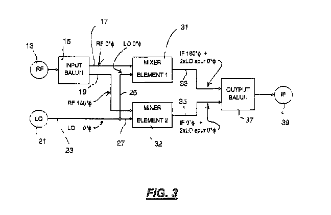
[00281 FIG. 3 is a diagram of a mixing circuit according to the invention;
[0029] FIG 4 is a graph of exemplary inputs and outputs of mixers according to
the
invention.
[0030] FIG. 5 is a diagram showing the pattern of thin-layered materials on a
substrate for a
mixer circuit according to the invention.
[0031] Detailed Description
[0032] For the purposes of promoting and understanding the principles
disclosed herein,
reference is now made to the preferred embodiments illustrated in the
drawings.
[0033] The lightweight mixer design described here is particularly applicable
to circuitry
used in satellites to process high-frequency wireless radio signals. Weight is
a particular
concern in orbital devices, due to the high cost of launch based on weight. An
exemplary
system is therefore shown herein on a satellite, although it will be
understood that the
invention may have a wide range of terrestrial uses as well.
[0034] Referring to FIG. 1, a satellite 100 is shown in orbit above the Earth
200 (or
potentially some other celestial body). The satellite 100 is provided with
antennae 101 and
102. According to the embodiment shown, antenna 101 receives one or more
wireless radio
signals indicated generally at 104 from an earth station indicated at A. These
radio signals
are normally high-frequency RF signals, i.e., with a frequency of 10 to 50
Gliz, and may be
television, audio, telephonic, data or electronic command communications to
the satellite, or
virtually any kind of communication signal, all of which are well known in the
art.
-6-
CA 02907223 2015-09-15
WO 2014/143956
PCT/US2014/028158
[0035] Satellite 100 also transmits a wireless high-frequency RF signal 105
back to earth
station B via antenna 102. The transmitted signals may also be any type of
transmission or
broadcast, such as a transmission of video from a camera on the satellite.
[0036] Most preferably, the satellite 100 is a communications satellite that
functions as a
"bent pipe" system, i.e., the satellite receives video, audio or data content
via the upload
signals 104, does some amplification, encryption, or other on-board processing
in the
satellite's internal circuitry, and then transmits the content back to Earth
in signals 105,
which can be at a frequency that is the same as or different from the
frequency of signals
104.
[0037] The satellite 100 has internal circuitry that receives and processes
the radio signals
104 and otherwise controls the operation of the satellite. The on-board
circuitry is preferably
in a hermetically sealed environment inside a carrier or protective case
inside the satellite
housing 107. The housing 107 is preferably of stainless steel and shields the
internal
components of the satellite from radiation and other potentially deleterious
influences found
in space. In addition, the satellite circuitry may be hardened by methods well-
known in the
art to prevent damage to the circuitry- by radiation outside the Earth's
atmosphere.
[0038] FIG. 2 shows a schematic diagram of the general internal operation of
the satellite
100. Receiver antenna circuitry 3 is connected with antenna 101 and receives
the radio
signal over a conductor linking them. Receiver antenna circuitry 3 transmits a
raw received
RF signal along a conductor to incoming signal process circuit 5, which
converts the RF
signal to a different, usually lower, frequency for processing on the
satellite. Generally,
down-conversion allows for easier manipulation, amplification or other
processing of the
content of the RF signal than at the high frequency at which it is received.
[0039] The converted RF sigqial is transmitted by conductor to the internal
satellite circuitry
7 for any kind of processing in accord with the function of the satellite,
e.g., as data, as
commands for control of the satellite 100 or as content re-transmission back
to Earth. For
example, where the content is television signals, the program content in the
RF signal may
be amplified and then possibly encrypted to yield a processed signal for
transmission.
_7_
CA 02907223 2015-09-15
WO 2014/143956
PCT/US2014/028158
[0040] The outgoing signal or signals generated by the internal satellite
electronics 7 are
transmitted over an electrical conductor to outgoing signal process circuit 9_
This circuitry 9
changes the frequency of the signal from internal electronics 7 to a
transmission signal at a
transmission frequency, usually higher than the incoming frequency. The
transmission
signal is sent by an electrical conductor to transmitting antenna circuitry
11_ which
wirelessly transmits it via antenna 102 to a receiver or receivers on Earth.
[0041] FIG. 3 is a more detailed block diagram of a circuit according to an
aspect of the
invention. This circuit is used in down-conversion circuitry of incoming
process circuit 5 or
in the outgoing signal process circuit 9,
[0042] A radio frequency (RF) signal source 13, e.g., the receiver antenna 101
and
associated circuitry 103, is connected to an input of an input balun 15 and
supplies an RF
signal to it. The input balun 15 has two outputs 17 and 19. Internally the
balun 15 splits the
RF signal. At output 17, the balun 15 outputs a first RF signal that has a
phase shift 4. of
zero (0) degrees, and at output 19, balun 15 outputs a second RE signal that
has been
delayed or otherwise processed so as to impart to it a 180-degree phase shift
4). The two RE
signals produced are therefore 180 degrees out-of-phase, or antiphase,
relative to each other.
[0043] A local oscillator (LO) 21 provides a -sinusoidal local-oscillator
signal LO to the
circuit on conductor 23, which has a simple branch into two conductors 25 and
27, which
both carry a respective split LO signal. Both of the LO signals have a phase
shift 4. of zero
degrees, i.e_, no phase shift, and are perfectly in phase with each other.
[0044] The frequencies of the LO and RF signals are above 1 GHz. Generally,
the circuit
shown is used with Ka band (26.5 to 40 GHz signal) downconverters and
receivers. It is also
scalable to other frequency applications, such as K band (20 to 40 GHz) or lc
band (12 to
18 GHz) applications. For the receiving signal processing circuit 7. the RF
signal preferably
has a frequency in the range from 10 to 40 GHz, and most preferably a
frequency of
approximately 30 GHz, and the LO signal has a frequency in the range from 5 to
20 GHz,
and most preferably a frequency of approximately 9.5 GHz.
[0045] Mixer element 1, indicated at 31, has two inputs. One of the inputs is
connected with
line 17 and receives the first FS signal from it with zero-degrees phase shift
(IL The other
-8-
CA 02907223 2015-09-15
WO 2014/143956
PCT/US2014/028158
input is connected with line 25 and receives one of the LO signals from it,
also with zero-
degrees phase shift 41. Mixer element 2, indicated at 32, has two inputs as
well. One of these
inputs is connected with line 19 and receives the second RF signal from it
with 180-degxees
phase shift cD, and the other input is connected with line 27 and receives
from it the other LO
signal with zero-degrees phase shift 41.
[0046] The mixer elements 31 and 32 constitute a 180 degree balanced set of
mixers, and
both have essentially identical configurations as will be described below. The
mixer
elements 31 and 32 mix the RF and LO signals supplied to them at the inputs
and produce
an IF signal provided at the respective mixer outputs 33 or 35. The mixer
output signals
each comprise a number of combined signals, including an IF signal that has a
frequency
that is the difference or the sum of the frequencies of the RF and LO signals.
Also, a number
of additional signals with other frequencies are typically produced by the
mixing process
and are present in the mixer output signals with the IF signal. These signals
include spur
signals formed as second and higher-order harmonics of the LO or RF input
signals.
[0047] FIG. 4 illustrates some of the signals applied to or produced by the
mixer elements
31 and 32 where the circuit is used to down-convert 30 GHz RF signal 201 to a
lower
frequency by mixing with a 9.5 GHz LO signal 202. In that case, the mixer
output signal
includes the desired output signal, IF signal 203, which has a frequency of
20.5 GHz. The
mixer output signal also includes spurs and noise, including spur signal 204,
which is the
second order harmonic of the LO signal input to the mixer, with a frequency of
2 * 9.5 GHz
¨ 19 GHz, and disagreeably close to the desired IF signal at 20.5 GHz.
[0048] The mixer elements 31 and 32 both produce the IF signal 203 and the
second LO
harmonic 2*L0 spur signal 204 in their respective outputs. However, because
the mixer
elements 31 and 32 receive the respective RF input signals 180-degrees out of
phase with
each other, the resulting IF signals in the two mixer output signals are also
180-degrees out
of phase to each other. In contrast, the LO signals received by the mixer
elements 31 and 32
are in-phase with each other, i.e., zero degrees out-of-phase and the 2*L0
second harmonic
spur signals 204 are also in-phase with each other in the two mixer output
signals.
-9-
CA 02907223 2015-09-15
WO 2014/143956
PCT/US2014/028158
[0049] This difference in phase-shift of the desired IF signal and the second
LO harmonic
spur signal allows for removal of the spur signal. This is accomplished by
supplying the
mixer output signals along conductors 33 and 35 to two inputs of output balun
37, which is
configured to give a phase shift of 180 degrees to one of the signals at one
of its inputs, and
then to combine that phase-shifted signal with the signal from the other
input. The
combined-signal result is transmitted at the single output of balun 37.
[0050] The input signals to the balun 37 in the circuit of FIG. 3 include the
IF signals in
antiphase and the second spur signals in phase. When one of these mixer output
signals is
given a 180-degree phase shift, the result is that the IF signals are placed
in phase and the
spur signals are put 180-degrees out of phase. As a result, when the shifted
signal and the
other signal at the balun 37 input are combined, the out-of-phase spur sigials
partly or
totally cancel each other out. Any of the other noise or spur signals in the
mixer output
signals that are in-phase between the two mixer output signals (e.g., higher
order even
harmonics of the LO signal) will also cancel each other out in balun 37.
[0051] The IF signals, however, are 180 degrees out of phase in the mixer
output signals, so
when one IF signal is phase-shifted 180 degrees and the two signals are
combined, the IF
signals are combined in phase, resulting in a strong IF signal. A final balun
output signal,
including the IF signal, is transmitted by conductor to subsequent processing
of the IF signal
by circuitry on the satellite, or to be transmitted via an antenna, generally
indicated at 39.
[0052] The circuit of the invention is scalable to frequencies other than the
ranges of
frequencies described herein. This circuit is beneficial for eliminating spur
signals without
relying on heavy filters, and with a greater degree of precision. For example,
it is possible to
use the present circuit where the LO signal frequency is 9.8 GITz and the RF
signal
frequency is 30 GHz. The resulting IF signal frequency is 20.2 GI-Iz, while
the second LO
harmonic spur signal has a frequency of 19.6 GHz, a separation of only 0.6
GHz, which
would be very difficult to carve out with a filter. Nonetheless, the phase-
shifted mixing
circuit described here allows for effective mixing of the signals even where
the harmonic
spur frequency and the IF signal frequency are separated by as little as 0.5
or 0.6 GIL,
-10-
CA 02907223 2015-09-15
WO 2014/143956
PCT/US2014/028158
[0053] FIG. 5 is a detailed plan view of an embodiment of the mixer circuit
that has been
described more generally above. The baluns 15 and 37 and the mixer elements 31
and 32 are
generally indicated by the same reference numbers as in FIG. S, as are the
conductors or
contacts identified in FIG. 3.
[0054] The circuit shown is manufactured using a multi-layer thin-film
approach in which a
layered material is etched or otherwise selectively removed so as to form a
lightweight
circuit. The process and materials used are available from the company Applied
Thin-Film
Products, with a place of business at 3439 Edison Way, Fremont, CA 94538, and
a website
at wvvw.thinfilm.com. The use of a multilayer structure as shown allows the
use of a thick
support substrate, with no air gap below it, which is different from typical
balanced mixer
designs.
[0055] The circuit may be a single component as shown, or may be part of a
larger circuit.
The circuit can also be manufactured using microwave integrated circuit
technologies.
[0056] The circuit 41 is supported on a ceramic substrate sheet 43, preferably
of a consistent
thickness. The substrate material is typically polished alumina, with a
dielectric constant of
9.9.
[0057] The RF input 13 and the LO input 21 are thin film gold transmission
lines. The RF
signal input 13 connects with the input of input 180' balun 15. Input balun 15
is of known
design, and is comprised of gold film conductors overlying a layer of
polyimide material 45
on the substrate 43. Input balun 15 also has ground connections 47 that extend
through the
substrate 43 to contact ground on the other side of the substrate 43. Input
balun 15 splits the
incoming RF signal and produces balanced output such that the split RF signals
are
transmitted to respective gold-film lines 17 and 19, with the RF signal on
line 17 having a
180 degree phase shift, as described above. The balun 21 is constructed to
maximize its
performance at a set Fif frequency or frequency range, and its design may
include structure
that substantially prevents impedance from interfering with transmission of
the RF
The balun 15 in the embodiment shown can split and phase shift RF signals in a
frequency
range of 23 to 34 GHz, appropriate in the present embodiment configured for
use with an
-11-
CA 02907223 2015-09-15
WO 2014/143956
PCT/US2014/028158
PeF with a frequency of 30 GHz. The design of course can be modified for
different RF
frequencies if appropriate.
[00581 LO signal input contact 21 connects to gold-film line 23, which leads
to an LO
signal splitting structure 49, also of gold film. Splitting structure 49
includes adjustment
structures 51 and 53, which may be used to adjust the precise distance that
the LO signal
must travel to the mixer elements 31 and 32. A resistor 55 bridges the split
LO signal lines
25 and 27 and balances the split signals on lines 25 and 27. Line 25 proceeds
via jumper 57
to mixer element 31 and line 27 proceeds to mixer element 32, passing through
another
adjustment structure 59, which provides for smaller phase adjustment than
adjustment
structures 51 and 53_ Preferably this is done to ensure that the LO signals
are configured to
arrive at the mixers 31 and 32 substantially in phase with each other,
[0059] Mixer elements 31 and 32 are essentially identical configurations. The
mixer
structure is effectively all on the upper side of the substrate 43, not
suspended, without a
cavity in the structure. Each mixer 31 or 32 comprises a mixer input balun 61
connecting
with a diode 63,
[0060] Each of the mixer input baluns 61 has a single input connected with a
respective RE
signal line 17 or 19. The mixer input baluns 61 are also of gold film
overlying a layer of
polyimide material. The mixer input baluns 61 have access to ground through
vias 69, which
extend through to the other side of the substrate 43 to contact ground_
[0061] Diodes 63 are chips inserted into the circuit 41. The diodes 63 are
commercially
available crossover quad diodes connected between the mixer input baluns 61 to
respective
LO/IF diplexer baluns 65 through gold-film conductors 71. LO signal lines 25
and 27 also
each connect across a resistor 77 with respective diplexer baluns 65 and
supply the LO
signals thereto. Resistors 77 make the diplexer baluns 65 less sensitive to
the drive level of
the LO signals.
[0062] The LO/IF diplexer baluns 65 are also formed of gold film on a
polvimide layer 73,
and vias 75 extend through the substrate 43 and provide connection to ground
for the baluns
65_ The diplexer baluns 65 each has a balun loop 79 that is sized to
correspond to the diode
63 configuration and parameters, as is well known in the art.
-12-
CA 02907223 2015-09-15
WO 2014/143956
PCT/US2014/028158
[0063] The mixer output signals are each transmitted to respective outputs of
the diplexer
balms 65 to gold-film lines 33 and 35. As described above, the IF signals in
these mixer
output signals are out of phase relative to each other, and the second LO
harmonic spur
signals in the two mixer output signals are in phase relative to each other_
[0064] That situation continues until the mixer output signals reach the
output 180' balun
37. Balun 37 is also formed of gold film on a polyimide layer 81, and it has
vias 83 to
ground extending through the substrate 43. As described previously, the balun
37 introduces
a 180 degree phase shift to the first mixer output signal, making the spur
signals out-of-
phase, and the two mixer output signals are then combined so that the spur
signals cancel
each other without affecting the IF signals. The output balun 37 is configured
in the present
embodiment to process signals that fall in the frequency range of 16 to 24
GHz, suitable for,
e.g., an IF frequency of 20=5 GHz and a second TO harmonic of 19 GHz, as has
been
discussed herein. A balun with a different configuration suited to a different
functional
frequency range, e.g., a higher range, may be employed if circuit 41 is to be
used for a
higher frequency output, such as up-converting the frequency of an on-board
signal for
broadcasting.
[0065] Output balun 37 transmits the signal that is derived from combining the
mixer output
signals along conductor 85 to the IF contact 39, where the circuit 41 connects
with other
electronics, not shown, that process the IF signal or transmit it vvirelessly,
as has been
described above.
[0066] Commonly, mixer circuits are made with metal conductor patterns on both
sides of a
relatively thin substrate, with coupling through the substrate. The influence
of ground on,
e.g., balun structures of the underside of the circuit is prevented by
providing a separating
cavity between wound and the metal pattern on the substrate.
[0067] In contrast, in the present design, the coupling of the gold conductors
in the balm' or
mixer structures takes place in the polyimide layer, which is very thin, e.g.,
4 microns to 5
microns thick, preferably about 4.5 microns thick. The substrate used in the
present design
is a thicker substrate. e.g., 10 to 20 times thicker than usual, e.g.. 200 to
300 microns thick,
most preferably about 254 microns thick. This larger thickness separates the
ground on one
-13-
CA 02907223 2015-09-15
WO 2014/143956
PCT/US2014/028158
side of the substrate from the circuitry on the other side, eliminating the
need for a cavity or
air clearance, with the result that the structure is markedly stronger.
[0068] The mixer circuit described herein can be used in either upconversion
or
downconversion applications above one GI-1z. It therefore may be used
primarily as a circuit
in a device for receiving Tif signals or transmission of IF signals, or both.
It also should be
clear that the circuit may be used in combination with other equipment, e.g.
where
additional components receive an RF signal from an antenna, modify the signal
received,
and then pass the modified signal to the RF port of a circuit of the present
design. Similarly,
additional equipment may receive the IF signal output and modify it before
transmission,
e.g. by amplification of the signal with an electronic amplifier.
[0069] Although adopting a standard convention of referring to one input
signal as the RF,
the present invention is agnostic as to whether the RF signal is broadcast and
later received
via antenna, if it exists entirely within a contained system and is never
transmitted
wirelesslv before or after it is processed by a circuit or circuits as herein
described, or if it
undergoes one or more transformation steps before or after mixing by a circuit
as described.
The FT signal may contain additional frequencies in some instances, and may
use amplitude
or frequency modulation, and may otherwise vary widely in form.
[0070] It should also be noted that the present invention may be practiced in
several other
variations. For example, if additional mixing elements are desired, the
circuit may be
adapted to their use by providing additional parallel paths of RF and LO
signals to the
additional mixing elements, and then from the mixing elements to the final
output balun.
The signals provided to the various mixer elements are then adjusted such that
the vector
sum of the mixer products at the output balun results in substantial
cancellation of the LO
and 2*L0 output signals, while retaining the desired IF output signal.
[0071] Where the topography requires, two intersecting electrical paths in the
circuit may
avoid electrical contact by the use of jumpers, such as ribbon jumper 57 or
87.
[0072] It should be understood that terms used herein are intended as
descriptive rather than
limiting, and that, although the invention has been described in conjunction
with the specific
embodiment set forth above, those skilled in the art in light of the
disclosures set forth
-14-
CA 02907223 2015-09-15
WO 2014/143956
PCT/US2014/028158
herein may make many alternatives, modifications and variations therein
without deputing
form the spirit of the invention.
-15-