Some of the information on this Web page has been provided by external sources. The Government of Canada is not responsible for the accuracy, reliability or currency of the information supplied by external sources. Users wishing to rely upon this information should consult directly with the source of the information. Content provided by external sources is not subject to official languages, privacy and accessibility requirements.
Any discrepancies in the text and image of the Claims and Abstract are due to differing posting times. Text of the Claims and Abstract are posted:
| (12) Patent: | (11) CA 2908165 |
|---|---|
| (54) English Title: | CIRCUIT AND METHOD FOR INDEPENDENT CONTROL OF SERIES CONNECTED LIGHT EMITTING DIODES |
| (54) French Title: | CIRCUIT ET PROCEDE DESTINES A LA COMMANDE INDEPENDANTE DE DIODES ELECTROLUMINESCENTES CONNECTEES EN SERIE |
| Status: | Granted and Issued |
| (51) International Patent Classification (IPC): |
|
|---|---|
| (72) Inventors : |
|
| (73) Owners : |
|
| (71) Applicants : |
|
| (74) Agent: | SMART & BIGGAR LP |
| (74) Associate agent: | |
| (45) Issued: | 2021-09-28 |
| (86) PCT Filing Date: | 2014-03-27 |
| (87) Open to Public Inspection: | 2014-10-02 |
| Examination requested: | 2019-03-26 |
| Availability of licence: | N/A |
| Dedicated to the Public: | N/A |
| (25) Language of filing: | English |
| Patent Cooperation Treaty (PCT): | Yes |
|---|---|
| (86) PCT Filing Number: | 2908165/ |
| (87) International Publication Number: | CA2014050314 |
| (85) National Entry: | 2015-09-28 |
| (30) Application Priority Data: | ||||||
|---|---|---|---|---|---|---|
|
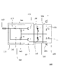
Described herein is a circuit and method for independent control of series connected light emitting diodes (LEDs). The circuit includes a first light emitting diode (LED) connected in series with a second LED. A current source is connected in series with the first LED and the second LED and a shunt circuit is connected in parallel with the first LED and the second LED. The shunt circuit includes a pair of serially connected resistors. The shunt circuit prevents inadvertent excitement of the LEDs due to leakage currents but minimally affect illumination characteristics of the LEDs. A pair of transistors is connected to the first LED and the second LED, respectively, and is biased using a set of bias resistors. A tri-state control signal switches on and off the pair of transistors and enables excitation of the first LED, the second LED or both via the current source.
La présente invention concerne un circuit et un procédé destinés à la commande indépendante de diodes électroluminescentes (DEL) connectées en série. Le circuit comprend une première diode électroluminescente (DEL) connectée en série avec une seconde DEL. Une source de courant est connectée en série avec la première DEL et la seconde DEL et un circuit de dérivation est connecté en parallèle avec la première DEL et la seconde DEL. Le circuit de dérivation comprend une paire de résistances connectées en série. Le circuit prévient toute excitation involontaire des DEL due à des courants de fuite, mais affecte minimalement les caractéristiques d'éclairage des DEL. Une paire de transistors est connectée à la première DEL et la seconde DEL, respectivement, et est polarisée à l'aide d'un ensemble de résistances de polarisation. Un signal de commande à trois états bascule la paire de transistors entre l'état passant et l'état bloqué et permet l'excitation de la première DEL, de la seconde DEL ou des deux par le biais de la source de courant.
Note: Claims are shown in the official language in which they were submitted.
Note: Descriptions are shown in the official language in which they were submitted.
2024-08-01:As part of the Next Generation Patents (NGP) transition, the Canadian Patents Database (CPD) now contains a more detailed Event History, which replicates the Event Log of our new back-office solution.
Please note that "Inactive:" events refers to events no longer in use in our new back-office solution.
For a clearer understanding of the status of the application/patent presented on this page, the site Disclaimer , as well as the definitions for Patent , Event History , Maintenance Fee and Payment History should be consulted.
| Description | Date |
|---|---|
| Letter Sent | 2024-03-27 |
| Inactive: First IPC assigned | 2022-01-06 |
| Inactive: IPC assigned | 2022-01-06 |
| Inactive: IPC expired | 2022-01-01 |
| Inactive: IPC removed | 2021-12-31 |
| Inactive: Grant downloaded | 2021-10-08 |
| Grant by Issuance | 2021-09-28 |
| Letter Sent | 2021-09-28 |
| Inactive: Cover page published | 2021-09-27 |
| Pre-grant | 2021-07-27 |
| Inactive: Final fee received | 2021-07-27 |
| Inactive: Submission of Prior Art | 2021-06-01 |
| Amendment Received - Voluntary Amendment | 2021-05-10 |
| Notice of Allowance is Issued | 2021-04-19 |
| Letter Sent | 2021-04-19 |
| Notice of Allowance is Issued | 2021-04-19 |
| Inactive: Approved for allowance (AFA) | 2021-03-31 |
| Inactive: Q2 passed | 2021-03-31 |
| Common Representative Appointed | 2020-11-07 |
| Amendment Received - Voluntary Amendment | 2020-09-04 |
| Examiner's Report | 2020-05-06 |
| Inactive: Report - No QC | 2020-05-06 |
| Inactive: IPC assigned | 2020-04-24 |
| Inactive: IPC assigned | 2020-04-24 |
| Inactive: First IPC assigned | 2020-04-24 |
| Inactive: COVID 19 - Deadline extended | 2020-03-29 |
| Inactive: IPC expired | 2020-01-01 |
| Inactive: IPC removed | 2019-12-31 |
| Common Representative Appointed | 2019-10-30 |
| Common Representative Appointed | 2019-10-30 |
| Letter Sent | 2019-03-29 |
| Request for Examination Received | 2019-03-26 |
| Request for Examination Requirements Determined Compliant | 2019-03-26 |
| All Requirements for Examination Determined Compliant | 2019-03-26 |
| Amendment Received - Voluntary Amendment | 2019-03-26 |
| Letter Sent | 2018-12-20 |
| Inactive: Correspondence - Transfer | 2018-12-18 |
| Inactive: Single transfer | 2018-12-10 |
| Change of Address or Method of Correspondence Request Received | 2018-01-12 |
| Amendment Received - Voluntary Amendment | 2017-05-10 |
| Inactive: First IPC assigned | 2015-10-19 |
| Inactive: Notice - National entry - No RFE | 2015-10-19 |
| Inactive: IPC assigned | 2015-10-19 |
| Inactive: IPC assigned | 2015-10-19 |
| Application Received - PCT | 2015-10-19 |
| National Entry Requirements Determined Compliant | 2015-09-28 |
| Amendment Received - Voluntary Amendment | 2015-09-28 |
| Application Published (Open to Public Inspection) | 2014-10-02 |
There is no abandonment history.
The last payment was received on 2021-03-26
Note : If the full payment has not been received on or before the date indicated, a further fee may be required which may be one of the following
Patent fees are adjusted on the 1st of January every year. The amounts above are the current amounts if received by December 31 of the current year.
Please refer to the CIPO
Patent Fees
web page to see all current fee amounts.
| Fee Type | Anniversary Year | Due Date | Paid Date |
|---|---|---|---|
| Basic national fee - standard | 2015-09-28 | ||
| MF (application, 2nd anniv.) - standard | 02 | 2016-03-29 | 2016-03-24 |
| MF (application, 3rd anniv.) - standard | 03 | 2017-03-27 | 2017-03-23 |
| MF (application, 4th anniv.) - standard | 04 | 2018-03-27 | 2018-02-23 |
| Registration of a document | 2018-12-10 | ||
| MF (application, 5th anniv.) - standard | 05 | 2019-03-27 | 2019-03-25 |
| Request for exam. (CIPO ISR) – standard | 2019-03-26 | ||
| MF (application, 6th anniv.) - standard | 06 | 2020-03-30 | 2020-04-24 |
| MF (application, 7th anniv.) - standard | 07 | 2021-03-29 | 2021-03-26 |
| Final fee - standard | 2021-08-19 | 2021-07-27 | |
| MF (patent, 8th anniv.) - standard | 2022-03-28 | 2022-03-14 | |
| MF (patent, 9th anniv.) - standard | 2023-03-27 | 2023-03-13 |
Note: Records showing the ownership history in alphabetical order.
| Current Owners on Record |
|---|
| FLEXTRONICS GLOBAL SERVICES CANADA INC. SERVICES GLOBAUX FLEXTRONICS CANADA INC. |
| Past Owners on Record |
|---|
| ALEXANDER ERMILOV |
| POMPILIAN TOFILESCU |

