Note: Descriptions are shown in the official language in which they were submitted.
CA 02910382 2015-10-26
WO 2014/177706
PCT/EP2014/059013
ANALYTICAL TEST METER
TECHNICAL FIELD
[0001] The present application relates generally to the field of medical
devices, and
particularly to analytical test meters, and related methods, for measuring an
analyte of a
patient sample, such as blood glucose or hematocrit.
BACKGROUND
[0002] The determination (e.g., detection or concentration measurement) of
an
analyte in a fluid sample is of particular interest in the medical field. For
example, it can
be desirable to determine glucose, ketone bodies, cholesterol, lipoproteins,
triglycerides,
acetaminophen or glycosylated hemoglobin (HbAlc) concentrations in a sample of
a
bodily fluid such as urine, blood, plasma or interstitial fluid. Such
determinations can be
achieved using an analytical test strip and test meter combination. For
example, a
diabetic patient conventionally tests his or her blood glucose using an
analytical test
meter and a disposable test strip. The user inserts the disposable test strip
into the
analytical test meter, then applies a drop of his or her blood to a sample-
receiving
chamber on the test strip. The analytical test meter applies test electrical
signals to the
blood in the sample-receiving chamber via electrodes and conductors on the
test strip,
and monitors resulting electrical signals. A processor in the analytical test
meter can then
determine the user's blood glucose (e.g., in mg glucose per dL of blood, or
mmol glucose
per L of blood) using the resulting electrical signals.
[0003] However, various factors can confound or interfere with such
determinations.
For example, U.S. Patent No. 7,390,667 to Burke et al. describes that reagents
in the
sample-receiving chamber are used to provide charge carriers that are not
otherwise
present in blood. Consequently, the electrochemical response of the blood in
the
presence of a given signal is intended to be primarily dependent upon the
concentration
of blood glucose. Secondarily, however, the electrochemical response of the
blood to a
given signal is dependent upon other factors, including temperature and
hematocrit
(HCT), the percentage by volume of red blood cells in the blood.
1
CA 02910382 2015-10-26
WO 2014/177706
PCT/EP2014/059013
[0004] U.S. Patent No. 8,343,331 to Choi describes a method of correcting
erroneous measurement results in a biosensor. A first voltage is applied to a
blood
sample on a test strip and a hematocrit value of the blood sample is
calculated using a
measured electric current value. A second voltage is then applied, and a
glucose level is
calculated using a second measured electric current value. The glucose level
is corrected
by using the calculated hematocrit value. However, this requires an accurate
measurement of hematocrit to provide results of a desired accuracy.
BRIEF DESCRIPTION OF THE DRAWINGS
[0005] Various features and advantages of the present invention will become
more
apparent when taken in conjunction with the following description and drawings
wherein
identical reference numerals have been used, where possible, to designate
identical
features that are common to the figures, and wherein:
[0006] FIG. 1 is a schematic representation of components of an exemplary
analytical test system including a analytical test meter and test strip;
[0007] FIG. 2 shows a schematic of an excitation source and a demodulator
for use
in the exemplary analytical test system of Fig. 1;
[0008] FIG. 3 shows a flowchart illustrating exemplary methods for
calibrating an
analytical test meter for use with an analytical test strip;
[0009] FIGS. 4A and 4B show a flowchart illustrating exemplary methods for
determining an analyte in a fluid sample;
[0010] FIG. 5 is a plan view of an exemplary test strip;
[0011] FIG. 6 is a dataflow diagram of an example of synchronous
demodulation;
and
[0012] FIG. 7 is a high-level diagram showing components of a data-
processing
system.
2
CA 02910382 2015-10-26
WO 2014/177706
PCT/EP2014/059013
[0013] The attached drawings are for purposes of illustration and are not
necessarily
to scale.
DETAILED DESCRIPTION
[0014] Even in analytical test meters that measure hematocrit (HCT) to more
accurately determine blood glucose, the hematocrit level measurement can be
affected by
parasitic electrical properties, e.g., parasitic capacitances, on printed
circuit boards in the
analytical test meter or in the test strip. Described herein are various ways
of detecting
and correcting for some such parasitic properties in various test meters for
various
analytes in various fluids.
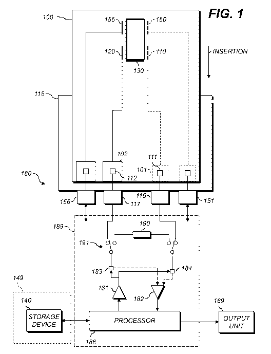
[0015] Fig. 1 is a schematic representation of components of an analytical
test
system according to various aspects. A "test set" or "test pairing" is such a
system
including a test strip 100 and an analytical test meter 180, e.g., a portable
analytical test
meter. The analytical test meter 180 can be, e.g., a hand-held test meter, and
can include
a housing. The analytical test meter 180 can also be clipped onto, or
otherwise fastened
to, a belt or strap, e.g., for placement place around the waist or over the
shoulder of a
user.
[0016] The analytical test system is adapted to determine an analyte in a
fluid
sample, e.g., a bodily-fluid sample. The analytical test meter 180 includes a
test-strip-
receiving module 115, also referred to herein as a "strip port connector" or
SPC. The
test-strip-receiving module 115 can include electrical or mechanical
structures adapted to
receive or retain a test strip 100. According to the exemplary version, the
test-strip-
receiving module 115 has at least first and second electrical connector pins
111, 112. For
purposes described herein, the term "pin" does not limit form factor; that is,
pins 111, 112
can be rigid pins, spring contacts, pogo pins, pressure contacts, solder
bumps, or other
electrically-conductive contacting devices.
[0017] The processor 186 controls operation of the analytical test system.
As
described herein, the processor 186 can include a microcontroller,
microprocessor, field-
3
CA 02910382 2015-10-26
WO 2014/177706
PCT/EP2014/059013
programmable gate array (FPGA), programmable logic array or device (PLA or
PLD),
programmable array logic (PAL) device, digital signal processor (DSP), or
other logic or
processing component adapted to perform functions described herein, or more
than one
of any of those, in any combination.
[0018] The exemplary test strip 100 has first and second electrodes 110,
120
operatively arranged with respect to a sample-receiving chamber 130, also
referred to
herein as an analyte chamber. The first electrical contact pad 101 is
electrically
connected to the first electrode 110. The first electrical contact pad 101 is
configured to
communicate an electrical response of the first electrode 110 to the
analytical test
meter 180 in electrical communication with the first contact pad 101, e.g., by
making
contact when the test strip 100 is properly inserted within the confines of
the test-strip-
receiving module 115. The test strip 100 can include a variety of electrical
contact
configurations for electrically connecting to the analytical test meter 180.
For example,
U.S. Pat. No. 6,379,513 discloses electrochemical cell connections, and is
hereby
incorporated by reference in its entirety.
[0019] The second electrical contact pad 102 is electrically connected to
the second
electrode 120 and is configured to communicate an electrical response of the
second
electrode 120 to the analytical test meter 180 when the analytical test meter
180 is in
electrical communication with the second electrical contact pad 102. The test-
strip-
receiving module 115 is arranged such that the first and second electrical
connector
pins 111, 112 make electrical connection with the first and second electrical
contact
pads 101, 102, respectively, when the test strip 100 is inserted into the test-
strip receiving
module 115. The processor 186 or related components are electrically connected
to
conductors 116, 117, which are electrically connected to pins 111, 112
respectively.
[0020] The processor 186 can detect the presence of the inserted test strip
100 by
sensing electrical properties between first and second electrical connector
pins 111, 112.
For example, the processor 186 can detect a change in capacitance between the
connector
pins 111, 112 when the test strip 100 is inserted. The test strip 100 can
include a third
4
CA 02910382 2015-10-26
WO 2014/177706
PCT/EP2014/059013
electrical contact pad (not shown) electrically connected to either the first
electrical
contact pad 101 or the second electrical contact pad 102. The test-strip-
receiving
module 115 can include a third electrical pin, and the processor 186 can
detect continuity
between two of the pins of the test-strip-receiving module 115 as indicating
insertion of a
test strip 100. The analytical test meter 180 can also include a mechanical,
optical, or
electromechanical element, e.g., a reed switch or optointerruptor, to
determine when the
test strip 100 has been properly inserted. The processor 186 can wait for a
test strip,
prompt for a strip, or take other actions until the test strip 100 is
detected, e.g., perform
calibration steps. The processor 186 can also enter a low-power mode, e.g., a
sleep
mode, until the presence of a test strip 100 is first detected. In an example,
the user
presses a button after inserting the test strip. The processor 186 detects
insertion of the
test strip when the button is pressed. This, and other examples in this
paragraph, can be
used for any strip detection described herein.
[0021] When the test strip 100 is detected, the processor 186 applies a
selected
electrical signal across the first and second electrical pins 111, 112 using
an excitation
source 181. The excitation source 181 can be a voltage source, current source,
arbitrary
waveform source, or other device adapted to produce electrical signals. The
processor
186 then measures a result electrical signal on pins 111, 112 using a
demodulator 182.
The demodulator 182 can include an analog to digital converter (ADC), sample-
and-hold
unit, mixer unit, or other device that is suitably adapted to measure
electrical signals. In
an example, a voltage is applied between the connector pins 111 and 112 and
the
resulting current through those pins is measured.
[0022] The excitation source 181 and the demodulator 182 can be connected
to
conductors 116, 117 through respective couplers 183, 184 that can include pass
transistors, RF couplers or gates, or other devices adapted to permit
excitation source 181
to apply signals to electrical conductors 116, 117 and to permit the
demodulator 182 to,
simultaneously or not, measure electrical properties of conductors 116, 117 or
signals
carried thereon. According to this exemplary embodiment, the couplers 183, 184
can
CA 02910382 2015-10-26
WO 2014/177706
PCT/EP2014/059013
include electrical shorts, so the output of excitation source 181 is connected
directly to
the input of the demodulator 182, and the processor 186 or demodulator 182 can
include
echo-suppression or echo-cancellation circuitry, logic, or code (not shown) to
remove the
output of the excitation source 181 from the received signal. In Fig. 1, the
couplers 183,
184 are represented graphically as squares. For clarity, connections to the
demodulator 182 are shown dashed.
[0023] The processor 186 processes the result electrical signal to detect
the fluid
sample and, if the fluid sample is present, to determine the analyte, e.g., to
determine
concentration or identity of the analyte. This determination is discussed
below. In
various embodiments, the processor 186 communicates an indication of the
determined
analyte, or other status infoimation (e.g., "no strip present" or "no sample
present") using
output unit 169. The output unit 169 can present various visible or audible
indicators
corresponding to the indication of the determined analyte. For example, the
output unit
169 can include a light that lights or blinks, a bell, beeper or buzzer that
sounds, a horn
that blows, an audio- or visual-reproduction system that activates (e.g., a
computer screen
that displays a pop-up error dialog), or a network interface that transmits
information
corresponding to the indication to a human-machine interface (HMI), server,
terminal,
smartphone, pager, or other computing or communications device. Any of these
devices
can operate to communicate the indication (e.g., the light can be defined by
an
illumination level that is proportional to a determined concentration of the
analyte).
[0024] Still referring to Fig. 1, an electrochemical (amperometric) method
for
measuring an analyte concentration in a fluid sample, e.g., a bodily-fluid
sample or an
aqueous sample, involves placing the sample into a reaction zone in an
electrochemical
cell (e.g., sample-receiving chamber 130) that has two electrodes (e.g.,
electrodes 110,
120) having an impedance that is suitable for the amperometric measurement.
The
analyte is allowed to react directly with an electrode (e.g., with one of the
electrodes 110,
120) or with a redox reagent to form an oxidizable (or reducible) substance in
an amount
that corresponds to the analyte concentration. The quantity of oxidizable (or
reducible)
6
CA 02910382 2015-10-26
WO 2014/177706
PCT/EP2014/059013
substance is then determined electrochemically. Various aspects accurately
determine the
point in time at which the sample is detected in the reaction zone. This
determination
permits an electrochemical waveform (e.g., voltage) to be applied immediately
after the
sample has been applied and accurately defines an incubation period or
reaction time. In
turn, the accuracy and precision of the assay are improved.
[0025] As will be discussed below, an enzyme can be present in the sample-
receiving chamber 130, or not. If present, the enzyme can assist in
transducing the
analyte in the fluid sample into a current, potential, or other quantity that
can be
measured electrically. The frequency and amplitude of signals from the
excitation
unit 181 can be selected according to various factors, e.g., the nature of the
fluid sample,
the nature of the analyte, or whether or not the electrodes to be used are
operatively
arranged with respect to an enzyme.
[0026] In an exemplary embodiment, more than two electrode pairs are
operatively
arranged with respect to the sample-receiving chamber 130. In the example
shown,
electrodes 150 and 155 are arranged to react with the fluid sample in the
sample-
receiving chamber 130. The electrodes 150, 155 are connected through
respective
conductors and pins to conductors 151, 156 respectively on the test-strip-
receiving
module 115. As represented by the arrows extending from the conductors 151,
156 into
the dummy load calibration circuit block 189, the electrodes 150, 155 can be
electrically
connected to the excitation source 181, the demodulator 182, the switching
unit 191, or
the processor 186. In various aspects, the electrodes 150, 155 do not have an
enzyme
coated on them or otherwise operatively arranged with respect to them. In an
example,
the electrodes 150, 155 are used for Hct measurement and are connected to the
excitation
source 181 and the demodulator 182 through the switching unit 191.
[0027] In various versions, first, a small, constant current source is
applied across the
electrodes 110, 120 of an electrochemical diagnostic strip and a potential
difference
between the electrodes 110, 120 is monitored. Before the sample is applied to
the sample-
receiving chamber 130 of the test strip 100, there is a dry gap between the
electrodes 110,
7
CA 02910382 2015-10-26
WO 2014/177706
PCT/EP2014/059013
120. Therefore, negligible current flows and the voltage difference between
the
electrodes 110, 120 increases. When a sample is applied to the test strip 100
and fills the
gap (sample-receiving chamber 130), the measured voltage decreases rapidly,
causing the
test time to be initiated. The processor 186 recognizes the decrease in
voltage as
indicative of a sample and automatically stops applying a constant-current
electrical
signal to the selected pins (e.g., pins 111 and 112). The processor 186 then
applies a
constant-voltage electrical signal to the selected pins. While the constant
voltage is
applied, current or charge can be measured as a function of time in order to
permit the
analyte concentration to be calculated.
[0028] In other embodiments, once a test strip has been inserted and that
insertion
has been detected, a bias (e.g., 400mV) is applied across the electrodes 110,
120. The
current between the electrodes 110, 120 is measured. When the current exceeds
a
selected threshold (e.g., 150nA), a fluid sample (e.g., a blood sample) is
detected. The
time at which the sample is detected is used as a reference time (T=0) for
calibration and
measurements relating to the inserted test strip.
[0029] The current measured a predetermined time after the constant voltage
is
applied is a measure of the analyte concentration, once the system has been
calibrated
using samples having known analyte concentrations. The duration of the
predetermined
time is not critical. For example, the duration of the predetermined time can
be at least
about 3 seconds when the fluid is blood and the analyte to be detected is
glucose. This
duration generally provides sufficient time to dissolve reagents and reduce an
amount of
mediator that is readily measurable. All things being equal, and when a sample
includes a
high level of hematocrit, longer times are needed. Therefore, the duration can
be <10
seconds. The same predetermined time can be used for multiple successive
measurements of respective samples. Further examples are given in US Patent
No.
6,193,873, incorporated herein by reference.
[0030] In various aspects, the test strip 100 can include opposed first and
second
sides (not shown). The second side can include an electrically-insulating
layer disposed
8
CA 02910382 2015-10-26
WO 2014/177706
PCT/EP2014/059013
over the second electrode 120. Each of the second electrically-insulating
layer and
second electrode 120 can include corresponding first and second cutout
portions that
expose corresponding areas of the first electrode 110 to define two
electrically-connected
electrical contact pads: pad 102 and a pad useful for detecting the test strip
100 by
determining connectivity. In various embodiments, the first and second cutout
portions
are arranged on opposing lateral sides of the test strip 100. Other
embodiments of a test
strip 100 are described below with reference to Fig. 5.
[0031] Electrodes 110, 120 can be stacked above and below the sample-
receiving
chamber 130. In various aspects, the second electrode 120 is electrically
insulated from
the first electrode 110 in a sandwiched format. In one version, the first
electrode 110
includes gold (Au) and electrode 120 includes palladium (Pd). The electrodes,
e.g.,
electrodes 110, 120, can be thin films. In various versions, the electrodes
include
conductive material formed from materials such as gold, palladium, carbon,
silver,
platinum, tin oxide, iridium, indium, and combinations thereof (e.g., indium-
doped tin
oxide or "ITO"). Electrodes can be formed by disposing a conductive material
onto
electrically-insulating layers by a sputtering, electroless plating, or screen
printing
process. In an example, sputtered gold electrode 110 is disposed over one side
of the test
strip 100, and sputtered palladium electrode 120 is disposed over the
remaining side.
Suitable materials that can be employed as electrically-insulating layers to
separate the
electrodes 110, 120 include, for example, plastics (e.g. PET, PETG, polyimide,
polycarbonate, polystyrene), silicon, ceramic, glass, and combinations
thereof, e.g., 7-
mil-thick polyester. Details of various exemplary test strips and measurement
methods
are provided in US Patent Application Publication No. 2007/0074977,
incorporated
herein by reference.
[0032] In various aspects, the sample-receiving chamber 130 is adapted for
analyzing small volume samples. For example, the sample-receiving chamber 130
can
have a volume ranging from about 0.1 microliters to about 5 microliters, or
0.2 to about 3
microliters, or about 0.3 microliters to about 1 microliter. To accommodate a
small
9
CA 02910382 2015-10-26
WO 2014/177706
PCT/EP2014/059013
sample volume, the electrodes 110 and 120 can be closely spaced. For example,
where a
spacer (not shown) defines the distance between the second electrode 120 and
the first
electrode 110, the height of the spacer can be in the range of about 1 micron
to about 500
microns, or between about 10 microns and about 400 microns, or between about
40
microns and about 200 microns. More details relating to exemplary test strips
are given
in US Patent No. 8,163,162, incorporated herein by reference.
[0033] A reagent layer (not shown) can be disposed within the sample-
receiving
chamber 130 using a process such as slot coating, coating by dispensing liquid
from the
end of a tube, ink jetting, and screen printing. Such processes are described,
for example,
in the following U.S. Patent Nos. 6,749,887; 6,689,411; 6,676, 995; and
6,830,934, each
of which is incorporated by reference herein. In various embodiments, the
reagent layer
is deposited onto an electrode (e.g., electrode 120) and includes at least a
mediator and an
enzyme. A mediator can be in either of two redox states which may be referred
to as an
oxidizable substance or a reducible substance. Examples of suitable mediators
include
ferricyanide, ferrocene, ferrocene derivatives, osmium bipyridyl complexes,
and quinone
derivatives. Examples of suitable enzymes include glucose oxidase, glucose
dehydrogenase (GDH) based on a pyrroloquinoline quinone co-factor, and GDH
based on
a nicotinamide adenine dinucleotide co-factor. One exemplary reagent
formulation for
the reagent layer is described in U.S. Application Ser. No. 10/242,951,
entitled, Method
for Manufacturing a Sterilized and Calibrated Biosensor-Based Medical Device,
published as U.S. Patent Application Publication No. 2004/0120848, which is
hereby
incorporated by reference in its entirety.
[0034] In an example, the electrode 120 is a working electrode formed by
sputtering
a Pd coating on a polyester base. A dry reagent layer is used and includes
buffer,
mediator, and enzyme, as described herein. A spacer between the electrodes 110
and 120
has a cutout area that defines an electrochemical cell (sample-receiving
chamber 130).
The spacer can be less than about 200 pm thick. The electrode 110 is a
reference
electrode formed by sputtering an Au coating on a polyester base. In this
example, a
CA 02910382 2015-10-26
WO 2014/177706
PCT/EP2014/059013
glucose oxidase/ferricyanide system is used to determine glucose
concentrations via the
following reactions:
Reaction 1: glucose + glucose oxidase-4
gluconic acid + reduced glucose oxidase
Reaction 2: reduced glucose oxidase +
2 ferricyanide¨* glucose oxidase + 2 ferrocyanide.
[0035] Ferricyanide ([Fe(CN)6]3-) is the mediator, which returns the
reduced glucose
oxidase to its catalytic state. Glucose oxidase, an enzyme catalyst, will
continue to
oxidize glucose so long as excess mediator is present. Ferrocyanide
([Fe(CN)6]4-) is the
product of the total reaction. Ideally, there is no ferrocyanide initially,
although in
practice there is often a small quantity. After the reaction is complete, the
concentration
of ferrocyanide (measured electrochemically) indicates the initial
concentration of
glucose. The total reaction is the sum of reactions 1 and 2:
Reaction 3: glucose + 2 ferricyanide¨>
gluconic acid + 2 ferrocyanide
[0036] "Glucose" refers specifically to I3-D-glucose. Details of this
system are
described in PCT Application No. WO 97/18465 and US Patent No. 6,444,115, each
of
which is incorporated herein by reference.
[0037] In an example, the analytical test meter 180 measures glucose level
and other
properties of a drop of blood on a test strip 100. One of those other
properties can be
hematocrit. HCT and glucose measurements are confounded, so measuring HCT
permits
determining glucose more accurately. The test strip 100 includes the sample-
receiving
chamber 130 that holds the drop of blood, pads 101, 102 to connect to
connector
pins 111, 112 in the analytical test meter 180, and the electrodes 110, 120
carrying
signals between the pads 101, 102 and the sample-receiving chamber 130. In
some
aspects, the test strip 100 includes at least one electrode used for measuring
HCT but not
glucose, and at least one electrode used for measuring glucose but not HCT (or
likewise
11
CA 02910382 2015-10-26
WO 2014/177706
PCT/EP2014/059013
for other pairs of analytes). In other aspects, the electrodes 110, 120 are
used for
measuring both HCT and glucose, either using successive electrical signals for
the
respective analytes, or using an electrical signal that permits determining
both glucose
and HCT from measured data corresponding to that electrical signal.
[0038] When the resistive component of the blood impedance is in the range
of tens
of KS2, parasitic capacitances on the order of fractions of pF on the printed
circuit boards
in the analytical test meter 180, in the test-strip-receiving module 115, in
the test
strip 100, and in any other components of the measurement path between the
excitation
source 181 and the demodulator 182 can affect accuracy and repeatability with
which the
analyte (blood glucose) can be determined. The effects of the parasitic
capacitances can
increase in severity as the frequency of measurement signals from excitation
source 181
increases.
[0039] In order, e.g., to compensate for these effects, the analytical test
meter 180
includes a dummy load calibration circuit block 189. In an exemplary
embodiment, the
dummy load calibration circuit block 189 is electrically connected to the test-
strip-
receiving module 115 and includes a dummy load 190, e.g., a resistor or a
precision
resistor (e.g., 221¶2, 0.1%). The dummy load 190 has selected electrical
characteristics,
e.g., impedance. The exemplary dummy load calibration circuit block 189 shown
also
includes the switching unit 191, the couplers 183, 184, the excitation source
181, the
demodulator 182, and the processor 186. As discussed above, the excitation
source 181
is adapted to selectively provide at least one electrical signal. The
demodulator 182 is
adapted to produce one or more demodulated signal(s) and the processor 186 is
connected to receive the one or more demodulated signal(s) from the
demodulator 182.
The demodulated signal(s) correspond to the electrical signal(s) from the
excitation
source 181 and to the electrical properties of the device(s) connected between
the
excitation source 181 and demodulator 182. In this way, the dummy load circuit
block 189 is configured to provide a dummy magnitude correction and a dummy
phase
12
CA 02910382 2015-10-26
WO 2014/177706
PCT/EP2014/059013
correction, and the memory block 149 is configured to store the dummy
magnitude
correction and the dummy phase correction, e.g., for later use by the
processor 186.
[0040] A switching unit 191 is adapted to selectively electrically connect
the
excitation source 181 to the demodulator 182 through either the dummy load 190
or the
first and second electrical pins 111, 112 of the test-strip-receiving module
115. In the
example shown, the switching unit 191 includes two electrically-controlled
single-pole
double-throw switches. One of those switches selectively connects the
excitation
source 181 to one of (a) a first terminal of the dummy load 190 or (b)
electrical connector
pin 112 (or pin 111) of the test-strip-receiving module 115. The other of the
switches
selectively connects an input of the demodulator 182 to one of (a) a second
terminal of
the dummy load 190 or (b) electrical connector pin 111 (or pin 112) of the
test-strip-
receiving module 115. Other configurations of switches can be used, e.g., a
single
double-pole double-throw, or an optoelectronic switch or reed relay. The
processor 186
can control the switching unit 191 electrically, optically, magnetically, or
in other ways.
[0041] A storage device 140 in memory block 149 stores data provided by the
processor 186, as discussed below. The storage device 140 can include, e.g., a
register,
memory, delay line, buffer, flip-flop, latch, disk, Flash memory device, or
other devices
describe below with reference to a storage subsystem 540, Fig. 7.
[0042] The processor 186 is adapted to concurrently cause the switching
unit 191 to
connect through the dummy load 190, cause the excitation source 181 to provide
a DC
signal (e.g., ground or another OV reference, or a selected bias), and record
first
respective value(s) of the demodulated signal(s) from the demodulator 182. The
processor 186 then determines a bias of the demodulator 182 using the first
respective
value(s) and stores the determined bias in the memory block 149, e.g., in the
storage
device 140. For example, the demodulator 182 can include a transimpedance
amplifier
and a synchronous demodulator. Applying a DC signal through the dummy load 190
removes time-varying components of the input, so any remaining signal
represents bias
13
CA 02910382 2015-10-26
WO 2014/177706
PCT/EP2014/059013
of the demodulator 182. Saving these values permits correcting for each noted
bias. This
is discussed further below with reference to step 320, Fig. 4A.
[0043] The processor 186 is further adapted to concurrently cause the
switching
unit 191 to connect through the dummy load 190, cause the excitation source
181 to
simultaneously provide both an AC signal and the DC signal, and record second
respective value(s) of the demodulated signal(s) from the demodulator 182.
From the
respective second value(s) and the determined bias of the demodulator, the
processor 186
determines a dummy magnitude correction and a dummy phase correction (e.g.,
phase
and gain modifiers of the analytical test meter 180). The processor 186 then
stores the
determined dummy magnitude correction and the determined dummy phase
correction in
the memory block 149, e.g., in the storage device 140. For example, the AC
admittance
of a blood sample is proportional to the hematocrit (HCT) in that sample, so
applying an
AC input simulates the AC signal used in test conditions. The resulting real
and
imaginary signals from the demodulator 182 are corrected by subtracting the
offset values
determined above and stored in the memory block 149, e.g., in the storage
device 140.
Using the corrected signals and known magnitude and phase characteristics of
the
dummy load 190, a gain factor and a phase offset are computed and stored.
[0044] The processor 186 is further adapted to detect the insertion of the
test
strip 100 in the test-strip-receiving module 115, as discussed above. The
processor 186
can detect insertion at any time, e.g., before applying the DC signal through
the dummy
load. The processor 186 is adapted to detect the insertion, and then
concurrently cause
the switching unit 191 to connect through the first and second electrical pins
111, 112,
cause the excitation source 181 to simultaneously provide both an AC signal
and a DC
signal (the same as the previously-applied signal or different), and record
third respective
value(s) of the demodulated signal(s). The processor 186 then determines phase
and gain
modifiers of the analytical test meter 180 with the inserted test strip 100
using the third
respective value(s), the determined dummy magnitude correction and the
determined
dummy phase correction (stored in the memory block 149, e.g., in the storage
14
CA 02910382 2015-10-26
WO 2014/177706
PCT/EP2014/059013
device 140), and the determined bias of the demodulator 182 (also stored in
the memory
block 149, e.g., in the storage device 140). The processor 186 then stores the
determined
phase and gain modifiers of the analytical test meter 180 with inserted test
strip 100 in the
memory block 149, e.g., in the storage device 140.
100451 As a result, calibration values useful for compensating electrical
effects of
components in the analytical test meter 180 and test strip 100 are stored in
the memory
block 149, e.g., in the storage device 140, and can be retrieved, as desired.
In various
embodiments, the processor 186 is further adapted to apply a selected
electrical signal
across the first and second electrical connector pins 111, 112 (having set
switching
unit 191 to connect through pins 111, 112) after the test strip 100 is
detected. The
processor 186 concurrently records fourth respective value(s) of the
demodulated
signal(s). The processor 186 then determines one or more corrected value(s)
corresponding to the fourth respective value(s) using the determined phase and
gain
modifiers of the analytical test meter 180 with the test strip 100, the
determined dummy
magnitude correction and the determined dummy phase correction, and the
determined
bias of the demodulator 182. The processor 186 retrieves these values from the
memory
block 149, e.g., from the storage device 140. The processor 186 is further
adapted to
process the determined corrected value(s) to detect presence of the fluid
sample and, if
the fluid sample is present, determine the analyte.
[0046] Fig. 2 shows a schematic of components of the dummy load calibration
circuit block 189, including the excitation source 181 and the demodulator
182, according
to various aspects. For clarity, in this example the excitation source 181 and
the
demodulator 182 are shown connected to only one switch in the switching unit
191 each,
so couplers 183, 184, Fig. 1, are not required. Also for clarity, electrical
connections
carrying control and data signals are shown by dashed lines; electrical
connections
carrying voltage or current signals are shown by solid lines. Throughout this
discussion,
any buffer can also be an amplifier, inverting or not, with a desired gain.
Filters can also
be used along with or in place of buffers to condition signals (e.g., low-pass
Butterworth
CA 02910382 2015-10-26
WO 2014/177706
PCT/EP2014/059013
filters). Control arrows pointing at one of two aligned switches indicate
control by the
processor 186 of both of those switches (e.g., switches 220, 222 and switches
260, 265)
with a single or with respective control signals.
[0047] The excitation source 181 is configured to provide voltage signals
(e.g., AC
or DC). In this example, the excitation source 181 includes a DC supply 210
and an AC
supply 212. The DC and AC supplies 210, 212 are connected via respective
switches 220, 222 to an adder 230, e.g., an op-amp voltage adder. The output
of the
adder 230 is provided to a buffer 240, which buffers the resulting voltage and
sends the
buffered voltage to the coupler 183, and subsequently to a switch in the
switching
unit 191. Other ways of providing voltage signals can be used, including table-
or
function-driven arbitrary-function or arbitrary-waveform generators (analog or
digital);
multipliers in place of the switches 220, 222 to multiply the voltages from
the DC and
AC supplies 210, 212, respectively, by selected weights >0; or selective
activation or
amplitude modulation of the DC and AC supplies 210, 212.
[0048] According to this embodiment, the demodulator 182 includes a
transimpedance amplifier 214 to measure current(s) and provide corresponding
voltage(s). In this example, the transimpedance amplifier 214 includes an op-
amp 250
and resistor 251 wired in a transimpedance amplifier configuration well known
in the
electronics art. For clarity, the second op-amp input is not shown; it can be,
e.g.,
connected to a reference voltage or wired in other ways known in the
electronics art for
the construction of transimpedance amplifiers. The voltage(s) from the
transimpedance
amplifier are provided to a demodulation block 216, optionally through a
buffer 252.
[0049] The demodulation block 216, e.g., a synchronous demodulation block
or
another appropriate type of demodulation block in demodulator 182, provides
demodulated signal(s) using the voltage(s). In various aspects, the
demodulation
block 216 includes two mixer units 217, 218 driven by respective control
signals from the
processor 186. Each of the mixer units 217, 218 can include a respective
switch 260,
265; a respective filter capacitor 261, 266, which can be part of a low-pass
or other filter;
16
CA 02910382 2015-10-26
WO 2014/177706
PCT/EP2014/059013
and a respective buffer 270, 275 to provide the output of the respective mixer
unit 217,
218. Mixer units 217, 218 can mix periodic signals and operate in the
frequency
domain. Further details of synchronous demodulation according to various
aspects are
discussed below with reference to Fig. 6.
[0050] In various aspects, the switches 260, 265 are analog switches that
multiply
their control signals with the input signal from buffer 252. In an exemplary
embodiment,
each control signal is a square wave. In various aspects, the switches 260,
265 have their
respective outputs fed back to the one of their inputs not connected to buffer
252. This
reduces noise on the outputs of the switches 260, 265.
[0051] Other mixer units or demodulators known in the electronics art can
also be
used. Analog-to-digital converters 280, 285 ("ADCs") can be used to convert
the analog
voltages from buffers 270, 275 into N-bit digital signals for the processor
186 (e.g., 8-,
10-, 12-, 16-, or 32-bit), or the processor 186 can receive analog inputs and
process them
in an analog domain or in a digital domain using an internal ADC (not shown).
[0052] In various aspects, the processor 186 provides respective control
signals to
the switches 260 and 265. The respective control signals are 90 out of phase
with each
other. In this way, the control signal designated as 0 phase can provide a
real bias
component, and the other control signal can provide an imaginary bias
component
discussed above. Specifically, in these aspects, the demodulated signal(s)
include a real-
component signal and an imaginary-component signal. In an example, switch 260
is
controlled by the 0 phase control signal to provide the real-component
signal.
Switch 265 is controlled by the 90 phase control signal to provide the
imaginary-
component signal.
[0053] As a result, the determined bias of the demodulator 182 includes a
real bias
component and an imaginary bias component. These components correspond
respectively to the real-component signal and the imaginary-component signal
when the
excitation source 181 is providing a DC signal, as described further below
with reference
17
CA 02910382 2015-10-26
WO 2014/177706
PCT/EP2014/059013
to the bias 318, Fig. 4A. The processor 186 is adapted to additively combine
(by adding
or subtracting) the real bias component and the imaginary bias component with
real
component(s) and imaginary component(s), respectively, of the second, third,
and fourth
respective value(s) of the demodulated signal(s) from demodulator 182. As a
result,
demodulator bias is substantially removed from the respective value(s),
advantageously
providing improved measurement accuracy.
[0054] In various of these aspects, the excitation source 181 provides a
first AC
signal from the AC supply 212. The analytical test meter 180, Fig. 1, further
includes a
phase delay unit 290. The phase-delay unit 290 can be included in the
processor 186 or
otherwise. The phase-delay unit 290 provides a lagged signal 900 in phase
behind the
first AC signal. (The phase-delay unit 290 can also provide a signal 90 in
phase ahead
of the first AC signal.) The two mixer units 217, 218 in the demodulator 182
are
controlled by the first AC signal (or a signal in phase therewith) and the
lagged signal,
respectively. The mixer units 217, 218 are thus operative to provide the real-
component
signal and the imaginary-component signal, respectively.
[0055] Fig. 3 shows a flowchart illustrating an exemplary method for
calibrating an
analytical test meter for use with an analytical test strip. In step 302, a
dummy magnitude
correction and a dummy phase correction of the analytical test meter are
determined
using a dummy load calibration circuit block of the analytical test meter. In
step 304, the
determined dummy magnitude correction and the dummy phase correction are
stored in a
memory block of the analytical test meter (e.g., memory block 140, Fig. 1). In
step 306,
an analyte is determined using the stored dummy magnitude correction and
stored
dummy phase correction.
[0056] In various aspects, the method further includes performing steps
307, 308,
and 309 before the determining-analyte step 306. Steps 307, 308, 309 can be
performed,
e.g., after step 304, or after step 302, or before either of step 302 or 304,
and the
execution of steps 302-304 and 307-309 can be interleaved.
18
CA 02910382 2015-10-26
WO 2014/177706
PCT/EP2014/059013
[0057] In step 307, insertion of a first analytical test strip in a test-
strip-receiving
module of the portable analytical test meter is detected. This can be as
described above,
e.g., detecting electrical characteristics, using a sensor, or receiving a
user input.
[0058] In subsequent step 308, phase and gain modifiers of the portable
analytical
test meter with the first analytical test strip inserted are determined. The
modifiers are
then stored, e.g., in memory block 149, Fig. 1. Various aspects of this step
are discussed
below with reference to modifiers 343.
[0059] In subsequent step 309, insertion of a second analytical test strip
in the test-
strip-receiving module is detected. Step 309 can include detecting removal of
the first
analytical test strip, or not.
[0060] In various aspects using steps 307, 308, 309, the determining-
analyte
step 306 further includes determining the analyte using the stored phase and
gain
modifiers of the portable analytical test meter with the first analytical test
strip inserted.
[0061] In an example, steps 302, 304, 307, and 308 are performed in the
factory
when the analytical test meter is produced. A typical or representative test
strip is
inserted and detected in step 307. The resulting values (dummy magnitude
correction,
dummy phase correction, and phase and gain modifiers) are stored, e.g., in
memory
block 149. Steps 309 and 306 are performed in the field, i.e., when the user
has the meter
and wishes to determine an analyte. The user inserts a test strip in the
analytical test
meter, and that test strip is detected in step 309. The analyte in the fluid
sample on the
test strip is then determined in step 306 using the values stored at the
factory. This
advantageously provides more accurate determination of the analyte without
requiring
that the analytical test meter take time to perform steps 302 and 308 for each
test strip.
[0062] In various aspects, steps 302, 304 are performed in the factory; or
steps 302,
304, 307, 308 are performed in the factory; or steps 302, 304 are performed in
the field;
or steps 302, 304, 307, 308 are performed in the field Steps 302, 304, 307,
308 can be
performed in the factory and then a repeat measurement check (e.g., of steps
302, 304, or
19
CA 02910382 2015-10-26
WO 2014/177706
PCT/EP2014/059013
of step 308, or of any of steps 320, 330, or 340, Fig. 4A) can be performed in
the field
every time a strip is inserted to determine whether the measurement has
drifted from the
factory calibration parameters.
[0063] Figs. 4A and 4B show a flowchart illustrating an exemplary method
for
determining an analyte in a fluid sample. Also shown are data produced by some
of the
steps and corresponding dataflow (dashed arrows). The steps can be performed
in any
order except when otherwise specified, or when data from an earlier step is
used in a later
step. For purposes of this exemplary method, processing begins with step 310.
For
clarity of explanation, reference is herein made to various components shown
in Figs. 1
and 2 that can carry out or participate in the steps of the exemplary method.
It should be
noted, however, that other components can be used; that is, the exemplary
method is not
limited to being carried out by the identified components. As represented
graphically by
the horizontal dotted line and the dotted-arrow labels, in an exemplary
embodiment
steps 310, 315, 320, 335, and 330 are part of step 302, Fig. 3; and steps 335,
340, 342,
345, 350, 354, 355 are part of step 306.
[0064] In step 310, an analytical test strip is received. The test strip
100 is received
upon insertion thereof into a test-strip-receiving module 115 of an analytical
test meter
180 so that first and second electrical contact pads 101, 102 exposed on the
test strip 100
electrically contact first and second electrical connector pins 111, 112 of
the test-strip-
receiving module 115, respectively. The test strip 100 includes a sample-
receiving
chamber 130 adapted to receive the fluid sample. The sample-receiving chamber
130 is
electrically connected between the first and second electrical contact pads
101, 102. In
an example, step 315 is next. In another example, this step is not performed;
instead,
step 342 (discussed below) is performed before step 335. In yet another
example,
processing begins with step 315, and step 310 is performed before step 335.
[0065] In step 315, using an electronics module (e.g., excitation source
181) of the
analytical test meter 180, a DC signal is applied through a dummy load to a
demodulator
182 that produces demodulated signal(s). The demodulated signal(s) can include
a real-
CA 02910382 2015-10-26
WO 2014/177706
PCT/EP2014/059013
component signal and an imaginary-component signal. Here and throughout this
disclosure, DC signals can have ripple and noise; it is not required that any
DC signal be
perfectly and exactly at one voltage, unvarying with time. Concurrently with
the
application of the DC signal, first respective value(s) of the demodulated
signal(s) are
recorded. Recording can be performed by the electronics module, a processor
186 of the
analytical test meter 180, or other devices in the analytical test meter 180.
Step 320 is
next.
[0066] In step 320, using the processor of the analytical test meter 180, a
bias 318 of
the demodulator is automatically determined using the first respective
value(s). This
processing can be performed by one processing resource or multiple processing
resources; processing resources can include hardware devices, firmware, or
software
programs executed on processors. In an example, the test meter includes a
digital signal
processor or other processing chip (e.g., processor 186). In various versions,
step 320
further includes storing the recorded first value (i.e., the one of the
recorded first
respective value(s)) corresponding to the real-component signal as a real bias
value and
the recorded first value corresponding to the imaginary-component signal as an
imaginary bias value. The determined bias 318 of the demodulator 182 thus
includes the
first bias value and the second bias value. Step 325 is next.
[0067] In an exemplary aspect, the demodulator 182 includes at least one
operational
amplifier (op amp) AC-coupled to a signal passed via switching unit 191. As a
result,
substantially no DC component is measured. The op amps can be biased by a
reference
voltage and thus operate with a dc offset, or otherwise. Since substantially
no DC
component is measured, and the DC signal has no substantially AC component,
the first
respective value(s) substantially correspond to offsets of the measurement
circuitry in the
demodulator and not to properties of the DC signal. Measuring the bias 318
thus
advantageously permits correcting for offsets in the demodulator 182 that
might
otherwise carry forward as errors in measurements of the analyte.
21
CA 02910382 2015-10-26
WO 2014/177706
PCT/EP2014/059013
[0068] In step 325, using the electronics module, a DC signal and an AC
signal are
simultaneously applied through dummy load 190 to the demodulator 182. Here and
throughout this disclosure, AC signals can be sinusoidal or not. For example,
AC signals
can be square waves or approximations of sinusoids formed by low-pass
filtering square
waves. Concurrently with the application of the signals, second respective
value(s) of the
demodulated signal(s) are recorded. Step 330 is next.
[0069] In step 330, using the processor 186, dummy corrections 333 are
automatically determined using the respective second value(s) and the
determined
bias 318 of the demodulator 182. The dummy corrections 333 include a dummy
phase
correction and a dummy magnitude correction. For example, the second value(s)
can be
adjusted according to the determined bias 318 of the demodulator 182, and the
dummy
corrections 333 of the analytical test meter can be determined using the
adjusted second
value(s). In aspects using real and imaginary components, step 330 can include
additively combining the real and imaginary bias values from bias 318 with the
second
value(s) before determining the dummy corrections 333. The dummy corrections
333
can include phase and gain modifiers of the analytical test meter 180. Step
335 is next.
[0070] In step 335, after receiving step 310 (or, in various aspects, after
detecting
step 342, discussed below), using the electronics module, the DC signal and an
AC signal
are simultaneously applied through the first and second electrical pins to the
demodulator
182. Third respective value(s) of the demodulated signal(s) as measured
through the
electrical pins 111, 112 are concurrently recorded. Step 340 is next.
[0071] In step 340, using the processor 186, phase and gain modifiers 343
of the
analytical test meter 180 with inserted test strip 100 are automatically
determined using
the third respective value(s), the determined dummy corrections 333 of the
analytical test
meter 180, and the determined bias 318 of the demodulator 182. In various
embodiments, step 340 includes automatically operating a switching unit 191 to
direct the
DC signal and the AC signal to the first electrical pin 111 and to connect the
second
electrical pin 112 to an input of the demodulator 182. In aspects using real
and imaginary
22
CA 02910382 2015-10-26
WO 2014/177706
PCT/EP2014/059013
components, step 340 can include additively combining the real and imaginary
bias
values from bias 318 with the third value(s) before determining modifiers 343.
Step 340
can also include adjusting the third value(s) according to the determined
dummy
corrections 333 before determining modifiers 343. Step 345 or, in various
embodiments,
step 341 or step 342 is next. In an example, steps 315, 320, 325, 330, 335,
340, 345, 350
are performed in that order. In another example, steps 315, 320, 325, 330,
342, 335,
340, 345, 350 are performed in that order.
[0072] In step 342, the insertion of the test strip 100 is automatically
detected. In
response to the detection, a selected electrical signal is applied in step
345. In various
aspects, steps 315, 320, 325, and 330 are performed before the test strip 100
is received
(step 310) and insertion of the test strip 100 is detected (this step 342). In
these aspects,
the bias 318 and the dummy corrections 333 can be determined before a test
strip 100 is
inserted, and the stored values of the bias 318 and the dummy corrections 333
can be
used to determine modifiers 343 and perform other computations (e.g., as in
step 350)
with respect to multiple test strips 100. In other aspects, steps 315, 320,
325, and 330 to
re-determine the bias 318 and the dummy corrections 333 are carried out for
each test
strip 100, e.g., upon detection of the insertion of the test strip 100. Step
342 can also be
performed before step 335. In an example, the bias 318 and the dummy
corrections 333
are to be determined after the detection, and step 342 is followed by Step
315. In another
example, the bias 318 and the dummy corrections 333 have been determined
before the
detection, and step 342 is followed by step 345.
[0073] In step 345, using the processor 186, a selected electrical signal
is
automatically applied across the first and second electrical connector pins
111, 112 after
the test strip 100 is received (step 310) or detected (step 342). The
processor 186 can
direct the electronics module to produce the signal, or produce it directly.
The signal can
be substantially the same as the AC and DC combined signal applied in step
340,
Fig. 4A; the selected electrical signal can include the DC signal and the AC
signal
applied in step 335 of measuring through the first and second electrical pins
111, 112.
23
CA 02910382 2015-10-26
WO 2014/177706
PCT/EP2014/059013
Concurrently, fourth respective value(s) of the demodulated signal(s) are
measured.
Step 345 can also be performed after a fluid sample has been detected, e.g.,
electrically or
via a user input control. Step 350 is next.
[0074] In step 350, using the processor 186, one or more corrected value(s)
353
corresponding to the fourth respective value(s) are automatically determined.
The
processor 186 determines the corrected value(s) using the determined phase and
gain
modifiers 343 of the analytical test meter 180 with test strip 100, the
determined dummy
corrections 333, and the determined bias 318 of the demodulator 182. Step 355
is next,
or, in various aspects, step 354.
[0075] In various aspects, in step 354, the corrected value(s) 353 are
automatically
processed, e.g., using the processor 186, to detect whether the fluid sample
applied to the
test strip 100 has filled the sample-receiving chamber 130. This detection can
be done,
e.g., by applying current and measuring voltage as described above or by
monitoring the
value(s) of the demodulated signal(s) for a decrease in impedance. The
demodulated
signal(s) can be transimpedance-amplifier output signals or other signals
indicative of
current, and an increase in the corrected value(s) corresponding to those
signal(s) over
time can indicate the sample-receiving chamber 130 has filled so is
conductive. Step 355
is next.
[0076] In step 355, the processor 186 automatically processes the corrected
value(s) 353 to determine the analyte in the applied fluid sample. This can be
as
discussed above.
[0077] In an example, step 341 is used. Steps 315, 320, 325, 330, 342, 335,
and 340
are performed, and resulting values are stored. These steps can be performed,
e.g., in the
factory when the analytical test meter is produced. In this example, step 340
is followed
by step 341. Steps 341, 345, 350, 354, and 355 can be performed in the field
when the
user inserts a test strip into the analytical test meter, as discussed above
with reference to
Fig. 3.
24
CA 02910382 2015-10-26
WO 2014/177706
PCT/EP2014/059013
[0078] In step 341, the processor detects the insertion of a second test
strip in the
test-strip-receiving module. This can be as discussed above with reference to
step 309,
Fig. 3. Step 341 is followed by step 345.
[0079] In step 345, a selected electrical signal is applied across the
first and second
electrical connector pins after the second test strip is detected. Fourth
respective value(s)
of the demodulated signal(s) are concurrently recorded. This can be as
discussed above.
[0080] In subsequent step 350, one or more corrected value(s) corresponding
to the
fourth respective value(s) are determined. This determination is made using
the stored
determined phase and gain modifiers 343 of the portable analytical test meter
with test
strip, the stored determined dummy magnitude correction, the stored determined
dummy
phase correction (both from the dummy corrections 333), and the stored
determined
bias 318 of the demodulator. This can be done as discussed above. Step 350 can
be
followed by step 354 or step 355.
[0081] In step 354, the corrected value(s) are processed to detect presence
of the
fluid sample on the second test strip. If the fluid sample is present, or if
step 354 is not
used, in step 355, the analyte is determined.
[0082] In an example, the analytical test meter 180 includes a
transimpedance
amplifier 214 and a synchronous demodulator (e.g., demodulation block 216)
similar to
those shown in demodulator 182, Fig. 2. The AC signal of steps 325, 335, and
345 is a
square wave filtered through a fourth-order Butterworth filter. The
demodulator 182 is
driven with 0 - and 90 -phase signals to produce real-component signals and
imaginary-
component signals. The deteimined bias 318 of the demodulator 182 includes
real and
imaginary bias values BR, BI, as discussed above. Each of the foregoing values
can be
stored. In steps 330, 340, and 350, the real and imaginary bias values BR, BI
are
subtracted from the corresponding values(s) of the demodulated signal(s).
CA 02910382 2015-10-26
WO 2014/177706
PCT/EP2014/059013
[0083] In this example, step 325 includes measuring real and imaginary
values of the
demodulated signal(s), denoted MR and MI. Step 330 includes forming bias-
corrected
values
CR = MR ¨ BR; CI = MI ¨ BI. (1)
Step 330 also includes receiving a known magnitude DM and phase DP of dummy
load 190. DM and DP can be stored in the memory block 149, e.g., in the
storage
device 140, Fig. 1, and can be programmed into the the memory block 149, e.g.,
into the
storage device 140, before the analytical test meter 180, Fig. 1, is shipped.
DM and DP
can be the same for all analytical test meters 180, or can be determined,
e.g., per meter or
per lot of meters. Step 330 includes computing a magnitude and phase CM, CP of
the
bias-corrected values as known in the mathematical art:
Mag(r, = Vr2 + = ;
12 Ph(r,i) = atan2(r,i) (2)
CM = Mag(CR, CI); CP = Ph(CR, CI) (3)
where atan2() is the four-quadrant arc-tangent. Step 330 further includes
computing the
dummy phase correction (AP) and dummy magnitude (gain) correction (AG).
Together,
these values are the dummy corrections 333. The AP and values AG values can be
stored, e.g., in step 304, Fig. 3. The computation is:
AP = CP ¨ DP (4)
AG = CM = DM (5)
[0084] Continuing this example, step 340 includes measuring MR and MI
values,
forming CR and CI values per (1), and computing CM and CP values per (3). The
CM
and CP values are then corrected using the dummy corrections 333 to form
corrected
values OM, OP:
OM = AG / CM (6)
OP = CP ¨ AP (7)
26
CA 02910382 2015-10-26
WO 2014/177706
PCT/EP2014/059013
Real and imaginary components OR, OI can be determined as
OR = OM cos(OP); OI = OM sin(OP). (8)
The OM and OP values are phase and gain modifiers 343 of the analytical test
meter with
test strip and can be stored. In various configurations, OM and OP represent a
complex
impedance in parallel with the fluid sample to be measured.
[0085] In this example, step 350 includes determining corrected value(s)
for the
fourth respective value(s). Stored BR, BI, AG, AP, OM, and OP values are
received.
For real and imaginary values FMR, FMI in the fourth respective value(s),
computations
are carried out as described above:
FCR = FMR ¨ BR (9)
FCI = FMI ¨ BI (10)
FCM = Mag(FCR, FCI); FCP = Ph(FCR, FCI) (11)
FOM = AG / FCM (12)
FOP = FCP ¨ AP (13)
FOR = FOM cos(F0P); FOI = FOM sin(F0P). (14)
Product terms PM, PP and difference terms SM, SP are then determined:
PM = OM = FOM (15)
PP = OP + FOP (16)
SM = Mag(OR ¨ FOR, OI ¨ FOI) (17)
SP = Ph(OR ¨ FOR, OI ¨ FOI). (18)
Using those terms, the corrected value(s) ZM, ZP are computed:
ZM = PM / SM (19)
ZP = PP ¨ SP (20)
27
CA 02910382 2015-10-26
WO 2014/177706
PCT/EP2014/059013
These corrected values can then be processed (step 355) to determine the
analyte. In
various configurations, these computations remove the previously-measured
parasitic
(OM and OP) from the measurement of parasitic in parallel with fluid sample
(FOM and
FOP) to determine the properties of the fluid sample alone (ZM and ZP).
[0086] Fig. 5 is a plan view of an exemplary test strip 100. The test strip
100 has a
planar design (e.g., using 2D printed conductive tracks 541, 542, 543, 544,
545) rather
than co-facial (opposing faces). The sample-receiving chamber 130 (dotted
outline) is
defined by a spacer (not shown) and covered with top tape (not shown). The
test strip
100 includes a plurality of conductive tracks 541, 542, 543, 544, 545
electrically
discontinuous from each other. Each of the conductive tracks 541, 542, 543,
544, 545
connects a respective contact pad 501, 502, 503, 504, 505 to a respective
electrode 571,
572, 573, 574, 575. The conductive tracks 542, 544 and their corresponding
contact
pads 502, 504 and electrodes 572, 574 are shown hatched only to permit
visually
distinguishing the various conductive tracks from each other. The electrodes
571, 572,
573, 574, 575, contact pads 501, 502, 503, 504, 505, and conductive tracks
541, 542, 543,
544, 545 can be printed from a conductive material, e.g., carbon, in a single
printing
operation, or can be fabricated in other ways (e.g., silk-screening).
[0087] Each electrode 571, 572, 573, 574, 575 is arranged at least
partially on a first
side 581 of the test strip 100, and is and at least partially adjacent to the
sample-receiving
chamber 130. That is, each electrode 571, 572, 573, 574, 575 is arranged so
that the
electrical properties of that electrode or its corresponding conductive track
can be
influenced by a sample in the sample-receiving chamber 130, or so that
electrical signals
through the respective conductive track 541, 542, 543, 544, 545 can be applied
to a
sample in the sample-receiving chamber 130. Each conductive track 541, 542,
543, 544,
545 can be adjacent to the sample-receiving chamber 130 on any side thereof,
or more
than one side thereof. The test strip 100 can also include other conductive
tracks (not
shown) that are not necessarily adjacent to the sample-receiving chamber 130.
In an
28
CA 02910382 2015-10-26
WO 2014/177706
PCT/EP2014/059013
example, an enzyme is deposited in an enzyme area overlapping the electrodes
571, 572,
573 but not overlapping electrodes 574, 575.
[0088] Fig. 6 shows a dataflow diagram of an example of synchronous
demodulation. The multipliers 660, 665 take as input a signal A=sin(o)t+0).
This can be,
e.g., a signal from buffer 252, Fig. 2. The cot term can represent a frequency
of an
excitation signal provided by excitation source 181, Fig. 2. The q term can
represent a
phase shift introduced by sample-receiving chamber 130, Fig. 1, or a fluid
sample
therein. The q) term can also represent an overall phase shift between the
excitation
source 181 and the demodulator 182, Fig. 1.
[0089] The multiplier 660 multiplies A by a known signal B=sin(cot). This
can be a
control signal from processor 186, Fig. 2, Signal B can be the fundamental
frequency in
a square wave. When a square wave is used, all odd harmonics of signal B are
also
multiplied with signal A by the multiplier 660. The multiplier 660 can include
a switch
that switches signal A and is controlled by signal B, e.g., switch 260, Fig.
2. Various
mixing units, including some using switches, are discussed in ANALOG DEVICES
tutorial MT-080 "Mixers and Modulators," Oct. 2008, incorporated herein by
reference.
[0090] The output of the multiplier 660 is an intermediate signal
0.5cos(0) - 0.5cos(2mt+4)).
This signal is filtered by the low-pass filter 668 to retain substantially
only the DC
component. That is, the cos(2(ot+0) term is removed from the intermediate
signal,
leaving only a DC signal with the value
0.5 cos().
This is a DC (substantially non-time-varying) value since it does not depend
on the value
of t. The low-pass filter 668 can include capacitor 261, Fig. 2. Odd harmonics
introduced if signal B is a square wave can be filtered out by the low-pass
filter 668. The
resulting DC component is an in-phase (or "real") component I.
29
CA 02910382 2015-10-26
WO 2014/177706
PCT/EP2014/059013
[0091] Similarly, the multiplier 665 multiplies signal A by a signal
C=sin(cot+90 ),
i.e., 90 out of phase with signal B. The multiplier 665 can include a switch
that switches
signal A and is controlled by signal C, e.g., switch 265, Fig. 2. The
multiplier 665
produces an intermediate signal which is filtered by the low-pass filter 669.
The low-
pass filter 668 can include capacitor 266, Fig. 2. The resulting DC component
is a
quadrature (or "imaginary") component Q.
[0092] The in-phase and quadrature components are then provided to
processing
function 686. Processing function 686 can be a mathematical function, and can
be
implemented as part of processor 186, Fig. 1, as a program running on
processor 186, or
using dedicated hardware communicatively connected with processor 186. The
processing function 686 can, e.g., compute magnitudes or phases per Eq. (2),
above. The
r and i parameters in Eq. (2) stand for "real" and "imaginary;" the in-phase
component
from low-pass filter 668 can be used for r and the quadrature component from
low-pass
filter 669 can be used for i. In various aspects, phase is computed and is
used to
determine Het. In various aspects, magnitude is computed and is used to
determine Hct.
Further examples are given in U.S. Application Ser. No. 13/857,280,
incorporated herein
by reference. Plot 690 shows an example of a signal Z with phase (I) plotted
on an in-
phase axis I and a quadrature axis Q,
[0093] In view of the foregoing, various aspects or embodiments process
measured
data to correct for errors that may be introduced by parasitic electrical
properties of the
test meter or test strip. A technical effect of various aspects is to provide
improved
measurement of hematocrit, and thus of blood glucose, permitting improved
dosing of
insulin to diabetic patients.
[0094] Throughout this description, some aspects are described in terms
that would
ordinarily be implemented as software programs. Those skilled in the art will
readily
recognize that the equivalent of such software can also be constructed in
hardware (hard-
wired or programmable), firmware, or micro-code. Accordingly, aspects of the
present
invention may take the form of an entirely hardware embodiment, an entirely
software
CA 02910382 2015-10-26
WO 2014/177706
PCT/EP2014/059013
embodiment (including firmware, resident software, or micro-code), or an
embodiment
combining software and hardware aspects. Software, hardware, and combinations
can all
generally be referred to herein as a "service," "circuit," "circuitry,"
"module," or
"system." Various aspects can be embodied as systems, methods, or computer
program
products. Because data manipulation algorithms and systems are well known, the
present
description is directed in particular to algorithms and systems forming part
of, or
cooperating more directly with, systems and methods described herein. Other
aspects of
such algorithms and systems, and hardware or software for producing and
otherwise
processing signals or data involved therewith, not specifically shown or
described herein,
are selected from such systems, algorithms, components, and elements known in
the art.
Given the systems and methods as described herein, software not specifically
shown,
suggested, or described herein that is useful for implementation of any aspect
is
conventional and within the ordinary skill in such arts.
[0095] Fig. 7 is a high-level diagram showing the components of an
exemplary data-
processing system for analyzing data and performing other analyses described
herein.
The system includes a data processing system 710, a peripheral system 720, a
user
interface system 730, and a data storage system 740. The peripheral system
720, the user
interface system 730 and the data storage system 740 are communicatively
connected to
the data processing system 710. Data processing system 710 can be
communicatively
connected to network 750, e.g., the Internet or an X.25 network, as discussed
below. The
processor 186, Fig. 1, can include or communicate with one or more of systems
710, 720,
730, 740, and can each connect to one or more network(s) 750.
[0096] The data processing system 710 includes one or more data
processor(s) that
implement processes of various aspects described herein. A "data processor" is
a device
for automatically operating on data and can include a central processing unit
(CPU), a
desktop computer, a laptop computer, a mainframe computer, a personal digital
assistant,
a digital camera, a cellular phone, a smartphone, or any other device for
processing data,
31
CA 02910382 2015-10-26
WO 2014/177706
PCT/EP2014/059013
managing data, or handling data, whether implemented with electrical,
magnetic, optical,
biological components, or otherwise.
[0097] The phrase "communicatively connected" includes any type of
connection,
wired or wireless, between devices, data processors, or programs in which data
can be
communicated. Subsystems such as peripheral system 720, user interface system
730,
and data storage system 740 are shown separately from the data processing
system 710
but can be stored completely or partially within the data processing system
710.
[0098] The data storage system 740 includes or is communicatively connected
with
one or more tangible non-transitory computer-readable storage medium(s)
configured to
store information, including the information needed to execute processes
according to
various aspects. A "tangible non-transitory computer-readable storage medium"
as used
herein refers to any non-transitory device or article of manufacture that
participates in
storing instructions which may be provided to processor 186 for execution.
Such a non-
transitory medium can be non-volatile or volatile. Examples of non-volatile
media
include floppy disks, flexible, disks, or other portable computer diskettes,
hard disks,
magnetic tape or other magnetic media, Compact Discs and compact-disc read-
only
memory (CD-ROM), DVDs, BLU-RAY disks, HD-DVD disks, other optical storage
media, Flash memories, read-only memories (ROM), and erasable programmable
read-
only memories (EPROM or EEPROM). Examples of volatile media include dynamic
memory, such as registers and random access memories (RAM). Storage media can
store
data electronically, magnetically, optically, chemically, mechanically, or
otherwise, and
can include electronic, magnetic, optical, electromagnetic, infrared, or
semiconductor
components.
[0099] Aspects of the present invention can take the form of a computer
program
product embodied in one or more tangible non-transitory computer readable
medium(s)
having computer readable program code embodied thereon. Such medium(s) can be
manufactured as is conventional for such articles, e.g., by pressing a CD-ROM.
The
program embodied in the medium(s) includes computer program instructions that
can
32
CA 02910382 2015-10-26
WO 2014/177706
PCT/EP2014/059013
direct data processing system 710 to perform a particular series of
operational steps when
loaded, thereby implementing functions or acts specified herein.
1001001 In an example, data storage system 740 includes code memory 741,
e.g., a
random-access memory, and disk 743, e.g., a tangible computer-readable
rotational
storage device such as a hard drive. Computer program instructions are read
into code
memory 741 from disk 743, or a wireless, wired, optical fiber, or other
connection. Data
processing system 710 then executes one or more sequences of the computer
program
instructions loaded into code memory 741, as a result performing process steps
described
herein. In this way, data processing system 710 carries out a computer
implemented
process. For example, blocks of the flowchart illustrations or block diagrams
herein, and
combinations of those, can be implemented by computer program instructions.
Code
memory 741 can also store data, or not: data processing system 710 can include
Harvard-
architecture components, modified-Harvard-architecture components, or Von-
Neumann-
architecture components.
[001011 Computer program code can be written in any combination of one or
more
programming languages, e.g., JAVA, Smalltalk, C++, C, or an appropriate
assembly
language. Program code to carry out methods described herein can execute
entirely on a
single data processing system 710 or on multiple communicatively-connected
data
processing systems 710. For example, code can execute wholly or partly on a
user's
computer and wholly or partly on a remote computer or server. The server can
be
connected to the user's computer through network 750.
[00102] The peripheral system 720 can include one or more devices
configured to
provide digital content records to the data processing system 710. For
example, the
peripheral system 720 can include digital still cameras, digital video
cameras, cellular
phones, or other data processors. The data processing system 710, upon receipt
of digital
content records from a device in the peripheral system 720, can store such
digital content
records in the data storage system 740.
33
CA 02910382 2015-10-26
WO 2014/177706
PCT/EP2014/059013
[00103] The user interface system 730 can include a mouse, a keyboard,
another
computer (connected, e.g., via a network or a null-modern cable), or any
device or
combination of devices from which data is input to the data processing system
710. In
this regard, although the peripheral system 720 is shown separately from the
user
interface system 730, the peripheral system 720 can be included as part of the
user
interface system 730.
[00104] The user interface system 730 also can include a display device, a
processor-
accessible memory, or any device or combination of devices to which data is
output by
the data processing system 710. In this regard, if the user interface system
730 includes a
processor-accessible memory, such memory can be part of the data storage
system 740
even though the user interface system 730 and the data storage system 740 are
shown
separately in Fig. 7.
[00105] In various aspects, data processing system 710 includes
communication
interface 715 that is coupled via network link 716 to network 750. For
example,
communication interface 715 can be an integrated services digital network
(ISDN) card
or a modem to provide a data communication connection to a corresponding type
of
telephone line. As another example, communication interface 715 can be a
network card
to provide a data communication connection to a compatible local-area network
(LAN),
e.g., an Ethernet LAN, or wide-area network (WAN). Wireless links, e.g., WiFi
or GSM,
can also be used. Communication interface 715 sends and receives electrical,
electromagnetic or optical signals that carry digital data streams
representing various
types of information across network link 716 to network 750. Network link 716
can be
connected to network 750 via a switch, gateway, hub, router, or other
networking device.
[00106] Network link 716 can provide data communication through one or more
networks to other data devices. For example, network link 716 can provide a
connection
through a local network to a host computer or to data equipment operated by an
Internet
Service Provider (ISP).
34
CA 02910382 2015-10-26
WO 2014/177706
PCT/EP2014/059013
[00107] Data processing system 710 can send messages and receive data,
including
program code, through network 750, network link 716 and communication
interface 715.
For example, a server can store requested code for an application program
(e.g., a JAVA
applet) on a tangible non-volatile computer-readable storage medium to which
it is
connected. The server can retrieve the code from the medium and transmit it
through the
Internet, thence a local ISP, thence a local network, thence communication
interface 715.
The received code can be executed by data processing system 710 as it is
received, or
stored in data storage system 740 for later execution.
CA 02910382 2015-10-26
WO 2014/177706
PCT/EP2014/059013
PARTS LIST FOR FIGS. 1-7
100 test strip
101, 102 contact pads
110 electrode
111, 112 connector pins
115 test-strip-receiving module
116, 117 conductors
120 electrode
130 sample-receiving chamber
140 storage device
149 memory block
150 electrode
151 conductor
155 electrode
156 conductor
169 output unit
180 analytical test meter
181 excitation source
182 demodulator
183, 184 couplers
186 processor
189 dummy load calibration circuit block
190 dummy load
191 switching unit
210 DC supply
212 AC supply
214 transimpedance amplifier
216 demodulation block
217, 218 mixer units
36
CA 02910382 2015-10-26
WO 2014/177706
PCT/EP2014/059013
220, 222 switches
230 adder
240 buffer
250 op-amp
251 resistor
252 buffer
260 switch
261 capacitor
265 switch
266 capacitor
270, 275 buffer
280, 285 analog-to-digital (ADC) converter
290 phase-delay unit
302, 304, 306 steps
307, 308, 309 steps
310,315 steps
318 demodulator bias
320, 325, 330 steps
333 dummy corrections
335, 340, 341, 342 steps
343 phase and gain modifiers
345, 350 steps
350 step
353 corrected value(s)
354, 355 steps
501, 502, 503, 504, 505 contact pads
541, 542, 543, 544, 545 conductive tracks
571, 572, 573, 574, 575 electrodes
581 side
37
CA 02910382 2015-10-26
WO 2014/177706
PCT/EP2014/059013
660, 665 multipliers
668, 669 low-pass filters
686 processing function
690 plot
710 data processing system
715 communication interface
716 network link
720 peripheral system
730 user interface system
740 data storage system
741 code memory
743 disk
750 network
[00108] The invention is inclusive of combinations of the aspects described
herein.
References to "a particular aspect" (or "embodiment" or "version") and the
like refer to
features that are present in at least one aspect of the invention. Separate
references to "an
aspect" or "particular aspects" or the like do not necessarily refer to the
same aspect or
aspects; however, such aspects are not mutually exclusive, unless so indicated
or as are
readily apparent to one of skill in the art. The use of singular or plural in
referring to
"method" or "methods" and the like is not limiting. The word "or" is used in
this
disclosure in a non-exclusive sense, unless otherwise explicitly noted.
[00109] The invention has been described in detail with particular
reference to certain
preferred aspects thereof, but it will be understood that variations,
combinations, and
modifications can be effected by a person of ordinary skill in the art within
the spirit and
scope of the invention.
38