Note: Descriptions are shown in the official language in which they were submitted.
CA 02910498 2015-10-28
Field Inversion Waveguide Using Micro-Prism Array
Inventors: James Babington, John Roberts
FIELD OF THE INVENTION
The present invention relates to optics, and more particularly, is related to
field inverting
waveguides.
BACKGROUND OF THE INVENTION
Known optical devices utilize diffraction gratings or beam splitters to couple
collimated
light out of a waveguide and into the eye of a user. The basic physics of
these structures result in
light being inefficiently coupled out of the waveguide from the consideration
of the eyebox
geometry. The beam splitters (essentially using reflection of the internal
waveguide rays to out
couple them) or diffraction gratings (using the corresponding phase of the
internal waveguide
plane waves to obtain transmitted/reflected diffraction orders) share the
property that the out
coupled collimated light is diverging with respect to the eyebox.
In standard waveguide helmet mounted display (HMD) technologies one of two
ways of
filling the eyebox is generally utilized. First, the original pupil may be
largely oversized so that
the eyebox can be filled with a small fraction of the image (and the rest
lost). This results in
relatively large collimators and waveguide substrates. A second way to fill
the eyebox is to use a
pupil replication technique, where an initial small pupil is input into the
waveguide. As the pupil
propagates down the waveguide it interacts with intermediate structures such
as diffraction
gratings or beam splitters that produce one or more copies of the original
pupil travelling in a
different direction to the original pupil. Pupil replication may be used to
create a large pupil in
both fields of view. The subsequent penalties resulting from pupil replication
include a non-
uniformity across the field and a banding of the replicated pupils as a
function of the field. These
1
CA 02910498 2015-10-28
limitations are inherent in pupil replicating designs. Therefore, there is a
need to overcome one
or more of the abovementioned shortcomings.
SUMMARY OF THE INVENTION
Embodiments of the present invention provide a field inversion waveguide using
a micro-
prism array. Briefly described, in architecture, the waveguide is configured
to convey
electromagnetic radiation from an ingress end to an egress end along an
optical path. The
waveguide includes an optically flat input surface disposed at the waveguide
ingress end, and an
exit surface disposed substantially opposite the input surface at the
waveguide egress end. The
exit surface includes an array of prisms projecting outward from or inward to
the exit surface.
The input surface and the exit surface are arranged substantially orthogonally
to the optical path.
Other systems, methods and features of the present invention will be or become
apparent
to one having ordinary skill in the art upon examining the following drawings
and detailed
description. It is intended that all such additional systems, methods, and
features be included in
this description, be within the scope of the present invention and protected
by the accompanying
claims.
BRIEF DESCRIPTION OF THE DRAWINGS
The accompanying drawings are included to provide a further understanding of
the
invention, and are incorporated in and constitute a part of this
specification. The drawings
illustrate embodiments of the invention and, together with the description,
serve to explain the
principals of the invention.
FIG. 1 is a schematic diagram showing an optical device under the first and/or
second
embodiments.
2
CA 02910498 2015-10-28
FIG. 2 is a schematic diagram of a portion of a waveguide exit structure
having an array
of projecting prisms under the first embodiment from a front perspective view.
FIG. 3 is a schematic diagram of a portion of a waveguide exit structure
having an array
of projecting prisms under the first embodiment from a side view.
FIG. 4 is a schematic diagram of a portion of a waveguide exit structure
having an array
of projecting prisms under the first embodiment from a rear perspective view.
FIG. 5 is a schematic diagram of a portion of a waveguide exit structure
having an array
of projecting prisms under the first embodiment from a front view.
FIG. 6A is a schematic diagram of a detail of a waveguide exit structure
having an array
of indented prisms under the second embodiment from a front perspective view.
FIG. 6B is a schematic diagram of a detail of a waveguide exit structure
having an array
of indented prisms under the second embodiment from a front perspective view,
including
subsurface features.
FIG. 6C is a schematic diagram of a detail of a waveguide exit structure
having an array
of indented prisms under the second embodiment from a top view.
FIG. 6D is a schematic diagram of a detail of a waveguide exit structure
having an array
of indented prisms under the second embodiment from a top view highlighting a
first prism
surface.
FIG. 6E is a schematic diagram of a detail of a waveguide exit structure
having an array
of indented prisms under the second embodiment from a top view highlighting a
second prism
surface.
FIG. 7 is a flowchart of an exemplary method for forming an optical device
according to
the first and second embodiments.
3
CA 02910498 2015-10-28
DETAILED DESCRIPTION
The following definitions are useful for interpreting terms applied to
features of the
embodiments disclosed herein, and are meant only to define elements within the
disclosure.
As used within this disclosure, "substantially" means "very nearly," for
example,
"substantially uniform" means uniform within normal manufacturing tolerances
as would be
expected by persons having ordinary skill in the art.
As used within this disclosure, the "eyebox" of an optical device is defined
as the amount
of allowable error in the eye relief position of a user that provides a clear
target image and full
field of view (FoV). The eyebox defines a range of motion for the eye of a
user that provides an
optimum target image and full FoV despite the eye being slightly in front of,
or slightly behind
the optimum eye relief position.
As used within this disclosure, "optically flat" refers to a surface that
deviates by no more
than one quarter of a wavelength from a perfect plane.
Reference will now be made in detail to embodiments of the present invention,
examples
of which are illustrated in the accompanying drawings. Wherever possible, the
same reference
numbers are used in the drawings and the description to refer to the same or
like parts.
Embodiments of the present invention include an array of micro prisms as an
exit
structure for an HMD waveguide, for example, a 4 x 4 array, among other
configurations. The
prisms may take the form of tilted roof prisms that implement two reflections
and a refraction to
invert the field of view of collimated light exiting a waveguide. The
embodiments serve to reflect
the light into the intended eyebox in a highly efficient way, providing a
simple structure for a full
color functioning display, and allowing control of both uniformity and pupil
banding that
4
CA 02910498 2015-10-28
commonly affect replicating waveguides. In addition, embodiments that perform
one field
inversion are also presented to further improve on existing replicating
waveguide structures.
The first and second embodiments employ a waveguide, for example, an HMD
waveguide, including a two-dimensional array of micro prisms as a principal
exit structure. A
micro prism is an optical imaging prism with spatial dimensions in the sub-
millimeter regime.
Under the first embodiment, the individual prisms each have the geometry of a
tilted roof prism.
In the ray optical picture for light propagating in the waveguide, the prisms
frustrate the total
internal reflection (TIR) within the waveguide. This is done in a very
specific manner,
implementing two reflections and a refraction of the light rays. For example,
rays within the
waveguide enter the individual micro prisms of the array through the bottom
prism face. The
rays then reflect off the two roof prism faces, one after the other. Finally,
the rays are refracted
out of the prisms from the prism face opposite the roof edge. This serves to
invert the field of
view (FoV) of collimated light exiting a waveguide. Fortuitously, this optical
structure enables
one to redirect the light into the intended eyebox of the user. In this way
the system becomes
highly efficient. Additionally, this embodiment provides a simple optical
structure for a full color
functioning system, and allows control of both uniformity and pupil banding
that commonly
affect pupil replicating waveguides. A second embodiment that performs one
field inversion is
also implemented to further improve on existing replicating waveguide
structures, described later
herein.
As noted above, previous solutions utilize diffraction gratings or beam
splitters to couple
collimated light out of a waveguide. These are naturally divergent structures
with respect to how
light is exiting the waveguide and propagating to the eyebox. By performing
field inversion as
with the present embodiments, the waveguide becomes extremely efficient while
keeping the
CA 02910498 2015-10-28
input pupil size small with respect to a standard replicating waveguide. The
embodiments may
also address larger fields of view and color systems.
The first and second embodiments each include a waveguide exit structure
having an
optical substrate patterned with a two-dimensional array of micro prisms.
Under the first
embodiment, the prisms project externally from the substrate. Under the second
embodiment, the
prisms project internally, forming indentations in the substrate.
In order to display a useful image to the observer, under the first embodiment
and the
second embodiment, an appropriate image source (incorporating any required
drive electronics)
and a collimating lens provide the image content. The image source may be
transmissive,
reflective or self-emissive. For indicative purposes only the image source
could take the form of,
but is not limited to, a Liquid Crystal Display (LCD), Active Matrix Thin Film
Transistor (AM-
TFT), Liquid Crystal on Silicon (LCoS), Digital Mirror Device (DMD), Cathode
Ray Tube
(CRT) or Organic Light Emitting Diode (OLED).
As shown in FIG. 1, in an optical device 100 under the first and second
embodiments,
collimator 120 receives incident light 105. The collimator 120 serves to map
the spatial extent of
an image (display) source into an appropriate angular range. As a non-limiting
example, a 30 x
20 field of view from the collimator may be considered representative. The
light 105 emitted by
the image source is converted into a collimated beam (parallel rays at some
angle relative to an
optical axis of the optical device 100), by the collimator 120, ensuring that
the virtual image, as
viewed by an observer, appears to originate from an infinite distance. The
input structure 130
couples a collimated beam into an optical substrate, such that the collimated
beam then
propagates along the waveguide 150 by total internal reflection. The optical
substrate allows
propagation of light by total internal reflection. The optical substrate may
be considered to be a
6
CA 02910498 2015-10-28
waveguide, not to be confused with the larger optical device 100 (input
structure, substrate &
output structure), which may also be referred to as a waveguide.
The input structure 130 may be, for example, a prism face or an embedded
mirror. It is
desirable that each pupil is coupled into the waveguide 150 by the collimator
120 in a one-to-one
fashion. An exit structure 200 frustrates the TIR and removes a portion of the
light out of the
substrate and into the eye 170 of an observer. Provided this condition is
simultaneously met for
all field angles, a complete virtual image appearing to be located at infinity
is generated at the
eyebox 160.
As described above, standard waveguide HMD technologies generally fill the
eyebox 160
by use of an oversized pupil, or by pupil replication. The first and second
embodiments instead
provide a field inversion technique that increases the overall efficiency of
the waveguide
structure 150 by ensuring that the eyebox 160 is filled with light from the
appropriate region of
the exit structure 200. To accomplish this, embodiments of the detailed prism
arrays described in
detail below employ re-direction of the propagating waves from the waveguide
150. In this
manner the current embodiments do not suffer from uniformity or banding
issues, and outside
world transmission through the waveguide 150 is solely dictated by the
relative intermediate flat
area to prism area.
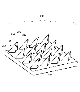
Under the first embodiment, shown by FIG. 2, an array 240 of prisms 250
projects
outward from a substrate 220 into a medium surrounding the waveguide 150 (FIG.
1), for
example, air. This is referred to as a Projected Tilted Prism Array (PTPA).
This substrate 220
is for fabrication purposes and is generally not fundamental to the design and
mode of
operation. The thickness of the substrate 220 depends upon fabrication,
mechanical and
environmental considerations.
7
CA 02910498 2015-10-28
FIG. 2 shows a detail of the basic form of the exit structure 200. The PTPA
forms a
sub area of one side of the waveguide substrate 150 exit surfaces 200. The
PTPA covers an
area appropriate to the desired FoV, exit pupil and eye relief and may be
determined by first
order optical principles (and is design specific). Typically the PTPA covers a
significant
fraction of the one substrate 220 face. A small boundary region surrounding
the optically
functional area of the PTPA may also be desired in order to mitigate against
mechanical
damage or misalignment. The opposite side, the input structure 130 (FIG. 1) is
typically
optically flat. The optical substrate 220 may be optical glass, plastic or any
medium which is
transparent to the wavelength of the radiation to be propagated. The two faces
confining the
radiation by TIR are parallel such that the substrate notionally has a
rectangular cross section.
In practice, it may be desirable to profile the edges of the substrate 220.
The thickness of the
substrate 220 is a design parameter and may be chosen almost arbitrarily,
however, in the
embodiment shown this is around 5mm.
The side geometry of the prism array 240 is presented in FIG. 3. The prism
array 240
typically includes a plurality of prisms 250 arranged two dimensionally in M
rows and N
columns. The array lattice need not necessarily be rectangular, nor regular
and remains a
design parameter. A first angle a between a rear corner edge 254 and the
substrate 220 is
typically an acute angle, for example, between 45 and 90 degrees, to preserve
the TIR of
incident light rays from the waveguide substrate 220. Angles closer to 90
degrees may result
in greater difficulty satisfying the TIR condition. Alternatively, if surfaces
252 and 253 are
mirror coated, the angle can be more freely chosen. A second angle 13,
measured between the
prism front surface 251 and the waveguide substrate 220 is typically obtuse,
for example,
between 110 and 150 degrees, and serves to change a nominal axis of the
exiting light rays.
8
CA 02910498 2015-10-28
These triangle angles a, 13 are relevant for the field inversion of a first
section of the field of
view, since effectively the pupil in the plane of the waveguide substrate 220
in FIG. 3 is
determined only by the angles shown therein. In FIG. 4 the back faces 252, 256
of the prisms
are shown. The two rear faces 252, 253 are nominally at 90 to one another and
together with
angle a from FIG. 3 constitute a tilted roof prism configuration. The two rear
faces 252, 253
are responsible for inverting the field of view in a second section, where the
second section
includes the remaining field of view not included in the first section. In
FIG. 5 the front
surfaces 251 of the PTPA prisms 250 are shown, from which the light rays are
refracted out
of the waveguide 150 and into the eye 160 (FIG. 1) of a user. The front
surfaces 251 of the
prisms 250 may be substantially planar, and configured in a generally
isosceles triangular
shape. As shown in FIGS. 2-5, the top portion of the front face 251 triangle
may be
somewhat truncated. This is because in the first section of the field of view
the light
propagates up the roof prism edge but is designed to stop before it reaches
the point vertex
that would otherwise be there. For example, once a FoV is defined, the prisms
may include
additional clearance for manufacturing and system purposes.
FIG. 3 shows a distance 340 and an angle 0 between the prism 250 front surface
251
and back corner 254. Similarly, FIG. 5 shows a prism spacing 501 and prism
height 502. The
distance 340, together with the angle 0, define an intermediate distance
between the back
surface 254 of one prism and the continuation of the front surface 251 of the
next prism. This
distance, for example, on the order of 0.5mm, together with the distance 501
in FIG. 5 (also
of the order of 0.5mm) determines the relative area of the base of the prism
to the unit cell
area of the underlying lattice. This in turn defines how efficient the PTPA
structure is, and at
the same time, how much outside world light is let through the intermediate
flat areas
9
CA 02910498 2015-10-28
contained in the unit cell. The one is inversely related to the other and is
design specific, but
typically > 50% of outside world light is desirable.
In contrast with the projecting prisms of the first embodiment, the second
embodiment includes a waveguide 150 (FIG. 1) with an exit structure 200 (FIG.
1) including
an array of indented prisms which may be used to perform a similar role to the
prisms of the
first embodiment, described above.
FIG. 6A shows a sectional view of an exemplary indented prism 650 as viewed by
an
observer looking at the indented surface of a waveguide exit structure
substrate 620. FIG. 6B
shows the same view as FIG. 6A, with the addition of dashed lines to indicate
features hidden
from view by the surface of the substrate 620, where 620 is analogous to the
exit structure
200 (FIG. 1) of the waveguide 150 (FIG. 1).
The indented prism 650 may be defined by five points, including four coplanar
points
[ABCD] on the surface of the substrate 620, and a vertex point [E] located
below the
substrate surface 620. The plane [ABCD] represents the surface of the
substrate 620, while
the vertex point [E] represents the maximum indentation depth of the prism 650
from the
substrate surface 620. This maximum depth is also illustrated by the point
[F], depicted
directly below point [A] from the perspective of the substrate surface 620.
FIG. 6A shows the
indentation as it would appear viewed from an arbitrary angle, while FIG. 6B
shows details
of the indentation vertex [E]. FIGS. 6C-6E show the indented prism 650 from an
overhead
perspective.
CA 02910498 2015-10-28
A first reflective surface 651 is a planar surface defined by the points
[CDE], formed
at a first angle with respect to the substrate surface 620. A second
reflective surface 652 is a
planar surface defined by the points [BCE], formed at a second angle with
respect to the
substrate surface 620. The first angle and the second angle may be
substantially the same
angle. The two reflective surfaces 651 and 652 are optically functional and as
such have low
RMS surface roughness (of the order of 5nm). Since these two surfaces 651, 652
are not
operating by total internal reflection, they may have standard mirror coatings
as per
determined by the substrate material. The angle between the first reflective
surface 651 and
the second reflective surface 652 is nominally 90 , and should be accurately
controlled. A
first rear surface 653 defined by the points [ADE] and a second rear surface
654 defined by
the points [ABE] may not be optically functional, and therefore the surfaces
may be made to
less stringent tolerances than the reflective surfaces 651, 652, for example,
regarding surface
roughness and/or flatness in comparison with the two reflective surfaces 651,
652. The length
of a single indented micro prism may be generally be in the sub millimeter
range, for
example, on the order of 0.5mm. An angle [<ACE] (in the region of 20 ) formed
between the
intersection [CE] of the two reflective surfaces 651, 652 and the substrate
plane 620 is a
design parameter which may depend on a refractive index of the substrate 620
and the
desired input/output angles of the incident light. Both optical plastics and
glasses are possible
as choices of substrate material, and may be chosen mostly for field of view
considerations.
The indented prism design is mostly unchanged due to this.
In alternative embodiments, the positions of vertices [A], [B], [D] and [E]
may be
design parameters which depend on the angles the non-optically functional
faces 653, 654 of
the prism 650 make with the substrate plane 620. These angles define the draft
angle of the
11
CA 02910498 2015-10-28
prism 650, defined as the angle [<EAF] between line [AE] and the normal [AF]
to the
substrate plane [ABCD], and may be adjusted as desired.
A plurality of indented prisms 650 may be configured as an array formed within
a
substrate surface 620 of a waveguide 150 (FIG. 1). The array structure
arrangement shares
exactly the same requirements as the first embodiment.
Preferably, first and second embodiments may be incorporated into systems 100
small
enough to be worn on the head as an HMD. The choice of substrate 220 materials
and the size
and area density of the micro prism array 240 may be arranged such that the
assembly is partially
transmissive to the outside world and can be tuned to a user requirement. This
enables the
observer to view the surroundings together with an infinity focused Augmented
Reality (AR)
display incorporating useful data overlaid on top of the output image.
The first embodiment facilitates full inversion of the FoV (horizontal and
vertical);
however fabrication of the prism structures may be complex. The second
embodiment facilitates
inversion of the FoV in one sense (horizontal or vertical, but not both), but
prism fabrication
using current manufacturing techniques may be more readily implemented.
FIG. 7 is a flowchart of an exemplary method 700 for forming an optical device
according to the first and second embodiments described previously. It should
be noted that any
process descriptions or blocks in flowcharts should be understood as
representing modules,
segments, portions of code, or steps that include one or more instructions for
implementing
specific logical functions in the process, and alternative implementations are
included within the
scope of the present invention in which functions may be executed out of order
from that shown
or discussed, including substantially concurrently or in reverse order,
depending on the
12
CA 02910498 2015-10-28
functionality involved, as would be understood by those reasonably skilled in
the art of the
present invention.
An optically flat input surface 130 (FIG. 1) disposed at a waveguide 150 (FIG.
1) ingress
end is formed, as shown by block 710. An exit surface 200 (FIG. 1) disposed
substantially
opposite the input surface 130 (FIG. 1) is formed at the waveguide 150 (FIG.
1) egress end, as
shown by block 720. An array of field inverting prisms 250 (FIG. 2)/650 (FIG.
6A) is formed
upon the exit surface 200 (FIG. 1), as shown by block 730. The input surface
130 (FIG. 1) and
the exit surface 200 (FIG. 1) are arranged substantially orthogonally to the
optical path, as shown
by block 740. The waveguide may be manufactured in modular fashion; the
collimator and
waveguide structure may be fabricated using standard optical glass shop
processes. This holds
true also for the input structure. The output structure may be more
challenging to fabricate,
however current micro-fabrication processes such as wet/dry etching or
embossing may be
employed.
In summary, the use of a two-dimensional prismatic array structure to
optically
implement two reflections to invert the field of view is a central feature of
the present invention.
It will be apparent to those skilled in the art that various modifications and
variations can be
made to the structure of the present invention without departing from the
scope or spirit of the
invention. In view of the foregoing, it is intended that the present invention
cover modifications
and variations of this invention provided they fall within the scope of the
following claims and
their equivalents.
13